MRS Advances © 201 Materials Research Society DOI: 10.1557/adv.201 .77
Seed Layer Assisted Hydrothermal Deposition of Low-resistivity ZnO Thin Films Eugene Chubenko1, Vitaly Bondarenko1, Amir Ghobadi2, Gamze Ulusoy3, Kağan Topalli3, Ali
Kemal Okyay2,3
1
Belarusian State University of Informatics and Radioelectronics, Minsk, 220013, Belarus
2
Department of Electrical and Electronics Engineering, Bilkent University, Bilkent, Ankara, TR 06800, Turkey
3
UNAM-National Nanotechnology Research Center and Institute of Materials Science and Nanotechnology, Bilkent University, Bilkent, Ankara, TR 06800, Turkey
ABSTRACT
In this work, we describe the combination of hydrothermal and atomic layer deposition (ALD) for growing low-resistivity ZnO polycrystalline continuous films. The effect of the thickness of ALD seed layers on the morphology of the hydrothermal ZnO films was studied. It was shown that ZnO films hydrothermally deposited on very thin seed layer consist of separate nanorods but in the case of 20 nm seed layer ZnO films transform to uniform continuous layers comprising of closely packed vertically aligned crystallites. Photoluminescence spectra were shown to exhibit broad band behavior in the visible range, corresponding to radiative
recombination processes via oxygen defects of ZnO crystalline lattice, and narrow band in the UV region, associated with band-to-band recombination processes. It was shown that the resistivity of the obtained ZnO films is decreased gradually with the increase of ZnO films thickness and determined by the presence of crystal lattice defects in the seed layer. INTRODUCTION
ZnO is a promising material for optoelectronics, photovoltaics and sensor applications [1, 2]. ZnO has unique combination of physical and chemical properties: wide direct band-gap, high exciton binding energy [3, 4] and transparency in optical and near IR-region [1, 5], prominent photocatalytic activity [6]. The key advantage of ZnO is that it can be fabricated by numerous techniques in the form of continuous films and nanostructures arrays even without lithography assistance [2, 3]. Molecular beam epitaxy, chemical vapor deposition, atomic layer deposition (ALD) and other vacuum based methods allow to deposit ZnO films with good crystalline quality. However, they become very expensive in the case of large substrates and have high operational temperature which is crucial for producing the integrated heterostructures [3]. Liquid phase electrochemical and chemical depositions are not so technologically demanding, but produce ZnO films with more structural defects and uncontrolled impurities [2, 7, 8].
Combination of vacuum based and liquid phase methods gives an opportunity to fabricate ZnO films with special structural and physical properties [2].
In this work, hydrothermal deposition as representative of liquid phase methods was applied to deposit thick ZnO continuous films on thin ZnO seed layers formed by ALD method on the Si and SiO2 substrates. It was supposed that seed layer could reduce the substrate
influence on morphology of hydrothermal ZnO films, provides uniformity, good adhesion and better precipitation for growing hydrothermal ZnO crystals which is useful for practical application of obtained hydrothermal ZnO films.
EXPERIMENTAL
Monocrystalline Si wafers of n-type and p-type conductivity with (100) crystallographic
orientation were used as substrates. Thin layer of SiO2 of approximately 100 nm in thickness was
formed on the surface of p-type Si wafers by thermal oxidation. No oxidation was used for the n-type Si wafers. Thin ZnO seed layers were formed by ALD method on the surface of substrates of both types. ALD of ZnO layers were carried out at 200 °C in a Savannah S100 ALD reactor. The thickness of seed layers was different and varied from minimal value – corresponding to 2
cycles of ALD process, to approximately 20 nm. Hereinafter these layers will be referred as
“thin” and “thick”, correspondingly. Thick ZnO layers with thickness up to several microns were hydrothermally deposited on the surface of ALD ZnO seed layers. Hydrothermal ZnO deposition
was carried out during 120 and 240 min from an aqueous 0.1 M ZnNO3 solution containing 0.1
M of hexamethylenetetramine (HMTA). pH at level of 5.2 (at 20 °C) was adjusted by HNO3. 50
ml thermostated glass autoclave was used for ZnO hydrothermal deposition. The substrates were placed horizontally with work side down on a PTFE holder. Substrates were immersed into the solution at 65 °C and then autoclave was heated to target temperature of 85 °C. After the process, completed substrates were rinsed in distilled water and dried in the air.
Hitachi-S4800 scanning electron microscope (SEM) was used to study the morphology and structure of the obtained ZnO films. XRA analysis was carried out with Bruker QUANTAX 200 EBSD analyzer. XPS spectra were obtained with Thermo Scientific K-alpha XPS
spectrograph operating at 1 kV of Argon ion beam energy level. For XRD analysis modified computerized DRON-3M X-ray diffractometer was used. Photoluminescence spectra were registered with spectroscopic complex based on Solar TII MS 7504i spectrograph equipped with CCD camera for signal registration. Photoluminescence was excited with 1 kW Xe lamp.
Monochromatic lines from the broad lamp spectra were cut by double monochromator Solar TII DM 160. The resistivity of the obtained ZnO films was measured by DC four-probe method on the potentiogalvanostat Metrohm Autolab PGSTAT302N based setup. Probes were made of copper and arranged in in-line configuration. The distance between probes was 1 mm.
Measurements were carried out only for samples formed on p-type Si with insulating SiO2 buffer
layer. As the thickness of studied ZnO films was much smaller than the distance between the probes, in the calculation of resistivity it was considered that electrical field extends to the entire thickness of the ZnO film and lower boarder of film is in contact with infinite insulating layer. All optical and electrical measurements were performed at the room temperature.
RESULTS AND DISCUSSION
ZnO “thin” seed layer was not distinguishable on the cross-section SEM images of the substrates. The concentration of Zn atoms in the “thin” film is below 1 at.% and could not be accurately determined because of low concentration and limitations of the method used. We believe that thickness of “thin” seed layer is no more than several angstroms. The thickness of “thick” seed layers measured on SEM images is approximately 16 nm. According to the results of XRA analysis concentration of Zn atoms in the “thick” ZnO seed layer is 36 at.% if ZnO is taken as 100 at.%, i.e. the composition of ZnO seed layer is not stoichiometric.
It is shown that the morphology of ZnO films formed by hydrothermal deposition on the surface of seed ZnO layers depends on the seed layer thickness. SEM images of the ZnO film hydrothermally deposited during 120 min on the “thin” seed layer are shown on Fig. 1. ZnO film
consists of individual ZnO crystals with prominent hexagonal shape typical for ZnO with wurtzite crystal lattice [3, 4]. The crystals are not well oriented and chaotically dispersed across the surface of the wafers. The obtained ZnO crystals are of relatively large diameter up to 3 μm. Typical twining of ZnO crystals [9, 10] of the so-called “dumbbell” type is also visible on the top-view SEM images (Figs. 1 b, d). It was found that the structure and size of deposited crystals
are the same for the substrates with and without SiO2 layer. The concentration of ZnO crystals on
the substrate with SiO2 layer is lower. It means that “thin” seed layer helps in the nucleation and
precipitation of hydrothermally formed ZnO crystals even on SiO2 surface. However, lack of
crystal structure of seed layer of that type not allowed oriented growth of ZnO crystals.
Figure 1. Cross-section and plain view SEM images of ZnO crystals hydrothermally deposited on the surface of monocrystalline Si wafer with “thin” seed layer with (a, b) and without (c, d) SiO2 buffer layer.
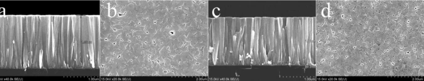
Seed ALD ZnO layer of 20 nm thickness is shown to have a strong effect on the structure of hydrothermal ZnO films. These ZnO films obtained on the Si wafers with “thick” seed layer consist of tightly packed ZnO crystallites and contain some pore-like gaps (Fig. 2). The thickness of ZnO film hydrothermally deposited during 120 min is approximately 1.5 μm. On the plain view SEM images, the slightly distorted hexagonal shape of the ZnO crystallites is visible which is characteristic for ZnO with wurzite type crystalline lattice [3, 4].
Figure 2. Cross-section and plain view SEM images of ZnO thin films hydrothermally deposited during 120 min on the surface of monocrystalline Si wafer with “thick” seed layer with (a, b) and without (c, d) SiO2 buffer layer.
ZnO thin films deposited on the “thick” seed layer contain approximately 50 at.% of zinc and 50 at.% of oxygen, i.e. they have stoichiometric composition. Excess of oxygen is not higher that 0.1-0.2 at.%. Hydrothermally deposited ZnO films usually have stoichiometric composition, determined by features of chemical reactions occurring during deposition [11]. According to
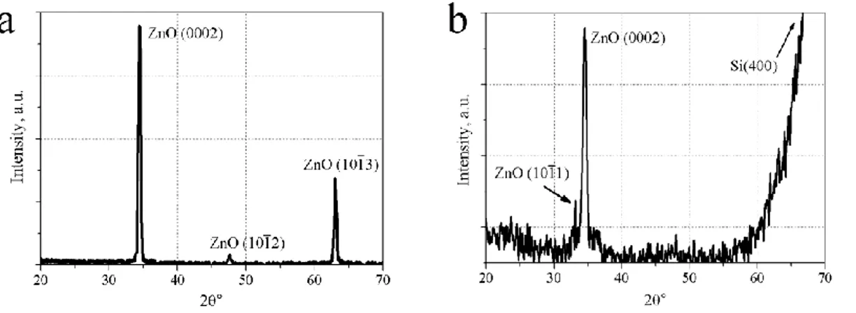
XRD data (Fig. 3, a) independently of Si wafers used (with or without SiO2 layers) fabricated
ZnO films are polycrystalline and consist of crystallites with hexagonal crystal lattice and have dominant crystallographic orientation (0002). It is important to note that XRD spectra of initial
seed layer also demonstrate dominant (0002) crystallographic orientation (Fig. 3, b) and peak associated with (1011) phase. Despite the fact that during hydrothermal deposition in the
presence of HMTA ZnO crystals grow in the direction [0002] perpendicular to wafer surface, the presence of phase (1011) and similar phases (1012) and (1013) in the seed layer and
hydrothermally grown ZnO means that the latter inherit structural properties of seed layer.
Figure 3. XRD spectra of ZnO thin film hydrothermally deposited during 120 min on Si wafer with “thick” seed layer (a) and ZnO “thick” seed layer itself (b). It should be noted that intensive dominant Si (400) peak can obscure (1013) ZnO peak.
XPS analysis revealed the presence of structural defects in the hydrothermal ZnO films (Fig. 4). XPS spectra of ZnO 1s oxygen band contain several components at 530, 531 and 532
eV corresponding to oxygen ions bounded to Zn atoms in ZnO crystal lattice (referred as OL on
Fig. 4), oxygen ion in the region with oxygen vacancies in ZnO crystal lattice (OV) and
chemisorbed oxygen (OC) [12]. The presence of OC band is associated with loosely bound
oxygen on the surface of ZnO film and attributed to the presence of OH– groups adsorbed during
hydrothermal ZnO deposition [11]. The intensity of OC band on XPS spectra increases with
thickness of hydrothermal ZnO film and it means that the concentration of hydroxyl group adsorbed at the ZnO surface increases as well. In the same time, relative contribution of OV
component in the intensity of oxygen 1s band decreases.
Figure 4. O 1s band on XPS spectra of ZnO films hydrothermally deposited on “thick” seed layer during 120 min (a) and 240 min (b).
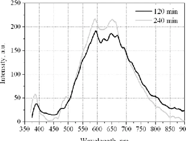
The photoluminescence spectra presented on the Fig. 5 revealed the presence of oxygen related defects in the ZnO crystal lattice. The wide band with two maximums at 580 and 650 nm at the photoluminescence spectra corresponds to irradiative recombination via energy levels in the ZnO band gap associated with oxygen vacancies in ZnO crystal lattice and interstitial oxygen atoms [5, 13]. Narrow band with the maximum at 380 nm is also presented on the spectra. It corresponds to the band-to-band irradiative recombination process as that wavelength is equivalent to 3.34 eV – the energy of ZnO band gap.
There is no significant difference in the intensity of photoluminescence bands of the ZnO films deposited during 120 and 240 min. As seen from Fig. 5 the intensity of the defect related broad band in the visible range for the sample with longer deposition time increased on 10-12 %, while the intensity of band-to-band recombination band increased on 55-57 %. This can be explained by the fact that concentration of crystal structure defects in the surface layers of ZnO films deposited during longer time is lower and their crystallinity is overall better. This correlates with the results of XPS analysis of the obtained ZnO films. The similar results were observed for
ZnO films deposited on Si and SiO2 substrates. It means that properties of hydrothermally
deposited ZnO films in the first order determined by the parameters of seed layer and are not correlate with the nature of underlying substrate materials.
Figure 5. Photoluminescence spectra of ZnO thin films hydrothermally deposited on “thick” seed layer during 120 and 240 min.
The resistivity of “thick” ZnO seed layer deposited by ALD was of 2·10-5
Ohm·cm as measured by four-probe method. However, the resistivity of double-layer structure consisting of “thick’ seed layer and ZnO film hydrothermally deposited during 120 and 240 min was 0.7 and 1.7 Ohm·cm, respectively. The ZnO seed layers were undoped that is why the relatively low resistivity can be defined only by high concentration of intrinsic defects forming donor levels in the oxide semiconductor band gap contributing to the majority charge carries concentration. Hydrothermally deposited ZnO films contain less structural defects and hence have higher resistivity. We suppose that ZnO crystallites deposited by hydrothermal deposition inherit structural defects of ALD seed layer. However, the concentration of those defects gradually dropped with the increase of film thickness. It is confirmed by change of the ratio of intensities of photoluminescence bands in visible and UV region for samples with different thickness and the results of XPS investigations. In other words, ZnO layers located on greater distance from the substrate and seed layer have better crystallinity.
CONCLUSIONS
The method of fabricating ZnO films by combination of ALD and hydrothermal deposition techniques is presented. It was shown that the morphology of hydrothermally deposited ZnO films depends on the thickness of ALD seed layer. Compact uniform ZnO films with the thickness of several microns could be formed only on seed layer of 20 nm thickness. Fabricated ZnO films are polycrystalline with dominant (0002) crystallographic orientation. It was found that the relatively low resistivity of the deposited ZnO films is defined by high concentration of intrinsic defects – primarily oxygen vacancies. Thick ZnO films deposited on the seed layer inherit structural defects of the seed layer however the concentration of those defects as well as electrical conductivity gradually decreased with the increase of ZnO film thickness. This also indirectly confirmed by the increase of the intensity of photoluminescence band with maximum at 380 nm. Deposited ZnO films also demonstrate photoluminescence in the visible range associated with recombination via oxygen related crystal lattice defects energy levels in the ZnO band gap. The compact uniform ZnO films fabricated by combination of hydrothermal and ALD techniques can be used in optoelectronic and photovoltaic devices. ACKNOWLEDGMENTS
The work has been funded as a part of the Belarus Government Research Program “Photonics, opto- and microelectronics”, Grant 2.1.02, and “Physical materials science, novel materials and technologies”, Grant 2.21.
REFERENCES
1. Ü. Özgür, D. Hofstetter and H. Morkoç, Proc. IEEE 98, 1255 (2010). 2. A. Kołodziejczak-Radzimska and T. Jesionowski, Materials 7, 2833 (2014).
3. Ü. Özgür, Ya. I. Alivov, C. Liu, A. Teke, M.A. Reshchikov, S. Doğan, V. Avrutin, S.-J. Cho and H. Morkoç, Appl. Phys. Rev. 98, 1 (2005).
4. T.C. Collins and R.J. Hauenstein, in Zinc oxide materials for electronic and optoelectronic
device applications, edited by C.W. Litton, D.C. Reynolds and T.C. Collins (John Wiley and
Sons Ltd., 2011), pp. 1-28.
5. A. Pimentel, E. Fortunato, A. Gonçalves, A. Marques, H. Águas, L. Pereira, I. Ferreira and R. Martins, Thin Solid Films 487, 212 (2005).
6. K.M. Lee, C.W. Lai, K.S. Ngai and J.C. Juan, Water Res. 88, 428 (2016). 7. D. Lincot, Thin Solid Films 487, 40 (2005).
8. M. Balucani, P. Nenzi, E. Chubenko, A. Klyshko and V. Bondarenko, J. Nanopart. Res. 13, 5985 (2011).
9. B.G. Wang, E.W. Shi and W.Z. Zhong, Cryst. Res. Technol. 33, 937 (1998).
10. Q. Yu, C. Yu, H. Yang, W. Fu, L. Chang, J. Xu, R. Wei, H. Li, H. Zhu, M. Li and G. Zou,
Inorg. Chem. 46, 6204 (2007).
11. S. Baruah and J. Dutta, Sci. Technol. Adv. Mater. 10, 013001 (2009).
12. M. Chen, X. Wang, Y.H. Yu, Z.L. Pei, X.D. Bai, C. Sun, R.F. Huang and L.S. Wen, Appl.
Surf. Sci. 158, 134 (2000).
13. W.C. Zhang, X.L. Wu, H.T. Chen, J. Zhu and G.S. Huang, J. Appl. Phys. 103, 093718 (2008).