D Zanato, S Gokden, N Balkan et al.
IOP PUBLISHING SEMICONDUCTOR SCIENCE AND TECHNOLOGY
Semicond. Sci. Technol. 22 (2007) 543–548 doi:10.1088/0268-1242/22/5/015
Scattering analysis of 2DEG carrier
extracted by QMSA in undoped
Al
0.25
Ga
0.75
N
/GaN heterostructures
S B Lisesivdin
1, S Acar
1, M Kasap
1, S Ozcelik
1, S Gokden
2and E Ozbay
31 Department of Physics, Gazi University, Ankara, Turkey 2 Department of Physics, Balikesir University, Balikesir, Turkey
3 Nanotechnology Research Center, Department of Physics, Department of Electrical-Electronics Engineering, Bilkent University, Ankara,
Turkey
E-mail: [email protected]
Received 10 December 2006, in final form 9 March 2007 Published 30 March 2007
Online at stacks.iop.org/SST/22/543
Abstract
Hall effect measurements on undoped Al0.25Ga0.75N/GaN heterostructures
grown by a metalorganic chemical vapour deposition (MOCVD) technique have been carried out as a function of temperature (20–350 K) and magnetic field (0–1.5 T). Magnetic field dependent Hall data were analysed using the quantitative mobility spectrum analysis (QMSA) technique. The mobility and density within the two-dimensional electron gas (2DEG) at the Al0.25Ga0.75N/GaN interface and within the underlying GaN layer were
successfully separated by QMSA. Mobility analysis has been carried out using both the measured Hall data at a single field and the extracted data from QMSA. Analysis of the temperature-dependent mobility of 2DEG extracted from QMSA indicates that the interface roughness and alloy disorder scattering mechanisms are the dominant scattering mechanisms at low temperatures while at high temperatures only polar optical phonon scattering is the dominant mechanism. Al0.25Ga0.75N/GaN interface related
parameters such as well width, deformation potential constant and
correlation length were also accurately obtained from the fits of the simple analytical expressions of scattering mechanisms to the 2DEG mobility.
1. Introduction
High electron mobility transistors (HEMTs) are widely used and accepted as the promising components of the high-speed electronics. HEMTs based on AlxGa1−xN/GaN heterostructures are the most interesting candidate since their description in 1993 [1] and demonstration of high-power operability [2]. Due to their large bandgap energy, large electron drift velocities, high conduction band discontinuity and high thermal stability, AlxGa1−xN/GaN heterostructures
can operate at high power and high temperature conditions with a 2DEG density and high mobility values as compared even with GaAs-based devices [3–6]. Even without an intentional doping, due to strong spontaneous and piezoelectric polarizations at the AlxGa1−xN/GaN interface, AlxGa1−xN/GaN heterostructures have 2DEG density with high sheet carrier density values [7, 8]. Since the mobility and density of the 2DEG in heterostructures are the key parameters related to the device performance, a detailed study of these parameters together with scattering mechanisms is of
critical importance for the device applications of AlxGa1−xN/GaN heterostructures. The analyses of carrier transport properties in AlxGa1−xN/GaN heterostructures have been reported in a number of papers [9–12]. In the majority of cases, these studies have been based on the analysis of the temperature dependent single magnetic field Hall measurements. In the mixed conduction (multi carriers) case, the standard resistivity and Hall effect measurements at a single magnetic field are of limited use because these measurements provide only averaged values of mobility and carrier density. Therefore,
Table 1. Material constants used in scattering calculations [20, 32].
High frequency dielectric constant Static dielectric constant
Electron effective mass LO-phonon energy LA-phonon velocity Density of crystal Electron wave vector
The electromechanical coupling coefficient ε∞ = 5.35 εs = 8.9 m∗ = 0.22m0 hω¯ = 0.092 eV ul = 6.56 × 10³ m s−1 ρ = 6.15 × 10³ kg m−3 k = 7.3 × 10⁸ m−1 K2 = 0.039 LA elastic constant TA elastic constant Alloy mole fraction
Lattice constant in the (0001) direction
cLA = 2.650 × 10¹¹ N m−2 cTA
= 0.442 × 10¹¹
N m−2 x =
0.25 c = 5.185 × 10⁻¹⁰ m
Volume of one atom
Alloy potential UAL = 2.36 × 10⁻¹⁹ V
single magnetic field Hall characterization is incapable of providing precise determination of the transport properties of AlxGa1−xN/GaN heterostructures since the charge carriers in bulk GaN and AlxGa1−xN layer can also contribute to the measurementsinadditiontotheinduced2DEGbypolarization at the interface.
To extract the correct transport parameters of the individualcarriersinthemultilayeredsemiconductormaterials such as AlxGa1−xN/GaN heterostructures, resistivity and Hall effect measurements are to be performed as a function of magnetic field. These measurements (variable field) allow the densities and mobilities to be simultaneously characterized for each of the multiple carrier species. Recently, the magnetic field dependent Hall data have been analysed successfully using QMSA technique, which is an effective technique for determining individual carriers in the multilayered semiconductors [13, 14]. Using the QMSA technique, the mobilities and carrier densities of each electron and hole species in bulk InN and GaN epilayers, and InP/InAlGaAs, HgCdTe, AlGaAs/GaAs and AlGaN/GaN heterostructures were investigated successfully by several groups [15–19].
In this work, firstly resistivity and Hall effect measurements of Al0.25Ga0.75N/GaN heterostructures grown by MOCVD technique have been carried out as a function of temperature (20–350 K) and magnetic field (0–1.5 T). To extract the individual mobilities and carrier densities of Al0.25Ga0.75N/GaN heterostructures, the measurement results were analysed using QMSA. Secondly, 2DEG mobility
analyses by taking into consideration the most relevant scattering mechanisms are carried out using both the measured Hall data and the extracted 2DEG data from QMSA. In both cases, Al0.25Ga0.75N/GaN interface related parameters were obtained and the differences between two cases were also discussed.
2. Scattering mechanisms
Scattering mechanisms of two-dimensional (2D) carriers in III–V heterojunctions are well described ([20], see references therein). The analytical expressions of the scattering mechanisms used in our calculations are summarized below. The material parameters used in the calculations are also listed in table 1.
2.1. Polar optical phonon scattering
At high temperatures, the mobility of a 2D carrier is mostly limited by polar optic phonon scattering. The expression of the mobility limited by the polar optic phonon scattering is given by Ridley as [21]
, (1)
where
. (2)
Here, ¯hω is the polar optic phonon energy, ε∞ and εs are the high and low frequency dielectric constants, respectively. m∗ is the effective mass.
2.2. Acoustic phonon scattering
At intermediate temperatures, the acoustic phonon scattering is another important scattering mechanism. In this work, we use the elastic acoustic phonon scattering model proposed by Ridley et al [22]. The acoustic phonon scattering is calculated by considering two scattering mechanisms, including deformation potential and piezoelectric scattering. The mobility expression of deformation potential is given by [22]
. (3)
In equation (3), ρ is the crystal density, ul is the longitudinalacousticphononvelocityandisthedeformation potential. The factor b is called the Fang–Howard expression [23] of wavefunctions for Hartree approximation of a triangular well and is given by [24]
. (4)
In equation (3), JDP(k) is the integral
(5) In this integral, qs is the two-dimensional reciprocal screening length which is defined as
(6) Here, f(0) is the occupation probability at the subband edge, which can be assumed that all screening is determined
S B Lisesivdin et al
by the lowest subband electrons [22]. F11(q) is the form factor of the ground-state Fang–Howard wavefunction [23].
In strongly polar materials such as GaN the acoustic phonons are strongly interacted by the piezoelectric effect. The mobility expression of piezoelectric scattering with a simplification of angular dependence is given by [22]
πε0εsh¯ 3k 1
µpe = eK2kBTm∗2 JPE(k). (7) In equation (7), K is the electromechanical coupling coefficient and given by [25]
. (8)
TA
In equation (8), εLA, εTA, cLA, cTA are the effective piezoelectric constants and the averaged elastic constants related to longitudinal and transverse acoustic phonons, respectively. The integral JPE(k) is in the form
(9) 2.3. Alloy disorder scattering
It is well known that the investigated 2D carriers populate near the AlxGa1−xN layer. The scattering of these electrons by conduction band disorder is called alloy disorder scattering. Kearley and Horrell [26] gave the mobility expression of alloy disorder scattering without screening effects as
16 eh¯ 3
µalloy
2 , (10)
AL
where x is the alloy mole fraction, 0 is the volume occupied by one atom and UAL is the alloy potential.
2.4. Background impurity scattering
Impurity scatterings for 2DEG carriers can be investigated in two parts; an ionized impurity scattering due to remote donors which is effective in modulation-doped structures and an ionized impurity scattering due to interface charges or simply background impurity scattering which is effective in all structures. In this work, because our samples are nominally undoped, we only use the background impurity scattering as an impurity scattering. The mobility of background impurity scattering is given by [27]
, (11)
e3m∗2NBI
where ε is the dielectric permittivity of GaN, and NBI is the 2D impurity density due to background impurities. The integral IB(β) is defined as
(12)
where
β = S0/2kF. (13)
In equation (13), kF is the wavevector on the Fermi surface, and S0 is the screening constant which is given for the degenerate case by Lee et al as [28]
. (14)
2.5. Interface roughness scattering
Interfaceroughnessisanimportantproblemforsemiconductor heterostructures [20]. Interface roughness can lead to the perturbation of electron energy [29]. Narrow quantum wells of AlxGa1−xN/GaN heterostructures are more sensitive to interface roughness that can lead to a large fluctuation in the quantized electron energies [30]. The mobility of interface roughness scattering is given by [20]
1 µIFR =
, (15)
IFR(k)
Figure 1. (a) Layer structure of Al0.25Ga0.75N/GaN heterostructures
sample that used in study. (b) Band structure of the sample. 2DEG is shown in detail in the inlet.
where is the lateral size of the roughness and
correlation length between fluctuations. The integral JIFR(k) in equation (15) is defined as
(16) where qs is the screening constant and given by [30]
(17) The form factor F(q) in equation (17) is given by [31] Scattering analysis of 2DEG extracted by QMSA in undoped Al0.25Ga0.75N/GaN
3. Experimental techniques
The sample investigated in this work was grown on a c-plane (0001) sapphire (Al2O3) substrate in a low-pressure MOCVD reactor. Prior to epilayer growth, the sapphire substrate was cleaned in H2 ambient at 1100 ◦C, and then a 25 nm thick low temperature (LT) GaN nucleation layer was grown at 500 ◦C. The reactor pressure was set to 50 mbar during the substrate cleaning and nucleation growth. After the deposition of the LT-GaN nucleation layer, the wafers were heated to a high temperature for annealing. For the sample, the two-step growth process was applied with the ramp time 2.5 min, and the annealing temperature 1100 ◦C. Approximately, a 2.5 µm thick GaN layer was deposited on the annealed nucleation layers using constant growth conditions. Finally, a 25 nm thick Al0.25Ga0.75N with 3 nm GaN cap layers was grown. All layers are nominally undoped. The details of the samples are given in figure 1.
For the resistivity and Hall effect measurements by the van der Pauw method, square-shaped (5 × 5 mm2) samples havebeenpreparedwithTi/Al/Ni/Auevaporateddotcontacts in the corners. Current was kept low to maintain ohmic behaviour, so the 2D electrons were in thermal equilibrium with the lattice. Current independence of mobility and the carrier density has been confirmed in the current interval of 1–500 µA. The measurements have been made over a
Figure 2. Experimental Hall mobility and sheet carrier density in
undoped Al0.25Ga0.75N/GaN.
temperature range 20–350 K using a Lakeshore Hall effect measurement system (HMS). At each temperature step, the Hall coefficient and resistivity have been measured for both current directions, both magnetic field polarization, and all possible contact configurations at 31 magnetic field steps between 0 and 1.5 T. The magnetic field dependent data have been analysed using QMSA software provided by Lakeshore. 4. Experimental results and analysis
4.1. Experimental results and quantitative
mobilityspectrum analysis
Resistivity and Hall effect measurements of Al0.25Ga0.75N/GaN heterostructures have been carried out as a function of temperature (20–350 K) and magnetic field (0–1.5 T). Figure 2 shows the temperature dependence of the sheet
carrier density and Hall mobility at 0.5 T in the temperature range of 20–350 K. At high temperatures, the mobility sharply decreases with increasing temperature while it is independent of temperature at low temperatures (below 100 K). The sheet carrier density can be accepted as temperature independent. These behaviours of sheet carrier density and mobility are typical of 2DEG structures. Above 100 K, Hall mobility decreases with increasing temperature with a temperature dependence of ∼T −3/2, which is a typical temperature dependence of phonon scattering mobility. The sheet carrier density still tends to be a constant, which is a further confirmation of the existence of 2DEG even at high temperatures. At room temperature, Hall mobility and sheet carrier density of the sample are 850 cm2 V−1 s−1 and 1.44 × 1013 cm−2, respectively. At 20 K, electron mobility is as high as 3013 cm2 V−1 s−1. In the nominally undoped AlxGa
1−xN/GaN heterostructures, such a high value of sheet carrier densities is due to the spontaneous and piezoelectric polarization fields [33, 34].
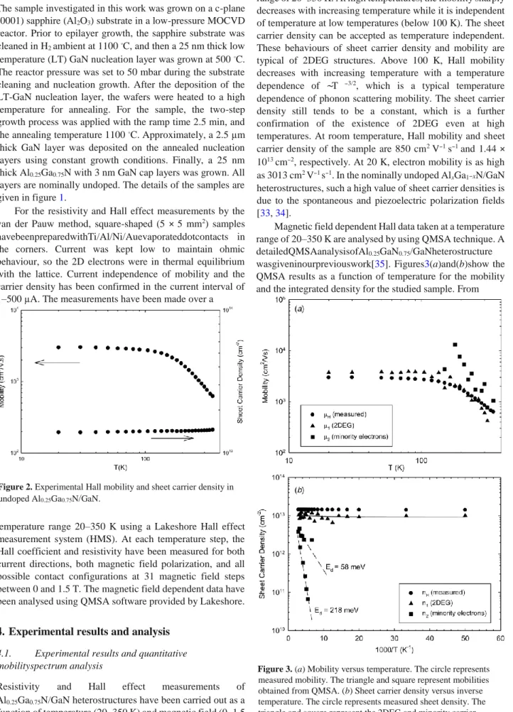
Magnetic field dependent Hall data taken at a temperature range of 20–350 K are analysed by using QMSA technique. A detailedQMSAanalysisofAl0.25GaN0.75/GaNheterostructure wasgiveninourpreviouswork[35]. Figures3(a)and(b)show the QMSA results as a function of temperature for the mobility and the integrated density for the studied sample. From
Figure 3. (a) Mobility versus temperature. The circle represents
measured mobility. The triangle and square represent mobilities obtained from QMSA. (b) Sheet carrier density versus inverse temperature. The circle represents measured sheet density. The triangle and square represent the 2DEG and minority carrier
S B Lisesivdin et al
densities obtained from QMSA, respectively. Lines show the proposed trends of the 2DEG and minority carriers.
figure 3(b), it can be clearly understood that both polarizationinduced 2DEG density (denoted with triangles) and thermally activated carriers (denoted with squares) contribute to the measured carrier density. At low temperatures, the extracted 2DEG mobility is slightly higher than the measured mobility. Below 100 K, the 2DEG mobility is temperature independent. Above 100 K, the 2DEG mobility is limited by lattice scattering mechanisms, which will be analysed in the next section. The extracted 2DEG density is independent of temperature at the whole studied temperature range, as is expected. Its proposed trend with temperature is shown by the solid line in figure 3(b). On the other hand, at the whole studied temperature range, the extracted 2DEG density is also lower than the measured sheet carrier density. The mobilities and densities of the minority carriers are highly temperature dependent. The thermally activated minority carriers (with activation energies of 58 and 218 meV) are originated from the donor levels of bulk GaN [13, 35]. 4.2. Mobility analysis
In this section the mobilities limited by the individual scatteringmechanisms, polaropticalphonon,acousticphonon,
Figure 4. (a) Measured and calculated (using the measured Hall
data) mobility versus temperature. (b) Extracted and calculated (using the extracted 2DEG density and mobility) mobility versus temperature.
alloy disorder, background impurity and interface roughness scatterings have been calculated from the expressions given in section 2 using the material parameters given in table 1. In the calculation, the background impurity (nimp) and lateral size ( ) were taken as 10−23 m−3 [36] and 2 × 2.58 × 10−10 m (for two monolayers) [32], respectively. The other parameters such as well width (Z0), deformation potential constant () and correlation length ( ) were used as adjustable parameters. Using the Mattheisen rule, the total mobility is then calculated as the combination of individual mobilities.
Firstly, we carried out the fit of the scattering expressions to the experimental mobility using the measured sheet carrier density taken at 0.5 T, as the usual approach. The calculated individual mobilities and the total mobility are given in figure
4(a). It can be seen from figure 4(a) that the total mobility fits quite well to the experimental data, taken at 0.5 T, using a well width of Z0 = 4 nm, a deformation potential constant of 12.5 eV and a correlation length of = 17.5 nm (corresponds to approximately 55 atomic spacing).
In general, the single field Hall effect data are widely used in the scattering analysis. However, since the single field Hall effect measurements provide only a weighted average of the mobility and carrier density, an accurate scattering analysis can only be carried out in the case of single carrier conduction. If the structure contains multiple carriers such as in AlxGa1−xN/GaN heterostructures, the single field Hall effect measurements would not lead to identify the correct transport parameters of the individual carriers. Secondly, the above calculations were, therefore, repeated using the extracted 2DEG mobility and 2DEG density from QMSA. The results are given in figure 4(b). A good agreement with the extracted 2DEG mobility is obtained using the fitting parameters as the well width of Z0 = 7.5 nm, the deformation potential constant of 8 eV and the correlation length of 5 nm (corresponds to approximately 30 atomic spacing).
The fitting parameters of the 2DEG obtained from the scattering analysis using the data extracted from QMSA show significantdifferencesfromthatoftheobtainedfromthesingle field Hall data. The former analysis has a smaller well width, a higher deformation potential value and a higher correlation length. Since the second analysis has been based on only the 2DEG mobility and density without the effects of the other carriers, the calculated parameters can be considered as more accurateparametersrepresentingtherealsamplefigures. Itcan be seen from figures 4(a) and (b) that the values of calculated individual mobility are also considerably different than that of the obtained from the single field Hall data. This indicates thatanyconclusiondrawnfromsinglefieldHallmeasurements may be highly misleading.
Considering the results (according to figure 4(b)), we conclude: (i) the low-temperature mobility is dominated by interface roughness and alloy disorder scattering mechanisms, and the background impurity scattering has also a
considerable influence on the 2DEG formed at the interface in undoped Al0.25Ga0.75N/GaN heterostructures. (ii) At high temperatures, the optical phonon scattering is the dominant mechanism, and the effects of interface roughness and alloy Scattering analysis of 2DEG extracted by QMSA in undoped Al0.25Ga0.75N/GaN
disorder scattering mechanisms have only small contribution to the mobility of 2DEG. It is interesting to note that our analyses show the acoustic phonon scattering has a negligible effect on the 2DEG mobility. However, the acoustic phonon scattering mechanism is, in general, found as a main scattering mechanism at intermediate temperature [37–39]. (iii) For Al0.25Ga0.75N/GaN heterostructures, the well width of Z0 = 7.5 nm, the deformation potential constant of 8 eV and the correlation length of 9.5 nm are obtained. These values are superior to the single-field measurement analysis results when compared with the Fermi wavelength well-width approximation [40] and the Hsu et al calculation for the deformation potential [9].
5. Conclusions
Hall effect measurements on undoped Al0.25Ga0.75N/GaN heterostructures grown by MOCVD have been carried out as a function of temperature (20–350 K) and magnetic field (0– 1.5 T). Magnetic field dependent Hall data were analysed using QMSA technique. QMSA successfully separated electrons in the 2DEG at the Al0.25Ga0.75N/GaN interface and electrons in the bulk GaN layer which contribute to the measurements in addition to the 2DEG at high temperatures. The mobility analysis has been carried out both using the measured Hall data at a single field (B = 0.5 T) and the data extracted from QMSA. The scattering analysis based on the extracted mobility and density of 2DEG formed at an Al0.25Ga0.75N/GaN heterointerface shows that the interface roughness and alloy disorder scattering mechanisms are the dominant scattering mechanisms at low temperatures while at high temperatures only the polar optical phonon scattering is the dominant mechanism. The values of well width, deformation potential and correlation length were found as 7.5 nm, 8 eV and 9.5 nm, respectively. Finally, it can be concluded that any conclusion drawn from single field Hall data or from any analysis based on single field Hall measurements would be highly misleading not only for AlxGa1−xN/GaN heterostructures but also for any semiconductor structures with multicarrier conduction.
Acknowledgments
This work is supported by the State of Planning Organization of Turkey under grant no. 2001K120590, and by TUBITAK under project nos. 104E090, 105E066, 105A005. One of the authors (Ekmel Ozbay) acknowledges partial support from the Turkish Academy of Sciences.
References
[1] Khan M A, Bhattarai A, Kuznia J N and Olson D T 1993
Appl. Phys. Lett. 63 1214
[2] Wu Y-F, Keller B P, Keller S, Kapolnek D, Kozodoy P, Denbaars S P and Mishra U K 1996 IEEE Electron Device
Lett. 17 455
[3] Wu Y-F, Keller B P, Parikh P, Kapolnek D, Denbaars S P and Mishra U K 1997 IEEE Electron Device Lett. 18 290
[4] Gaska R, Chen Q, Yang J, Osinsky A, Khan M A and Shur M S 1997 IEEE Electron Device Lett. 18 492 [5] Ruden P P, Albrecht J D, Sutandi A, Binari S C, Anastasiou K I, Ancona
M G, Henry R L, Koleske D D and Wickenden A E 1999
MRS Internet J. Nitride Semicond. Res. 4S1 G6.35
[6] Sheppard S T, Doverspike K, Pribble W L, Allen S T, Palmour J W, Kehias L T and Jenkins T J 1999 IEEE
Electron Device Lett. 20 161
[7] Ambacher O et al 2000 J. Appl. Phys. 87 334 [8] Bernardini F, Fiorentini F and Vanderbilt D 1997 Phys. Rev. B 56
R10024
[9] Hsu L and Walukiewicz W 1997 Phys. Rev. B 56 1520
[10] Miyoshi M, Ishikawa H, Egawa T and Jimbo T 2003
Phys. Status Solidi c 0 2091
[11] Cordier Y, Hugues M, Lorenzini P, Semond F, Natali F and Massies J 2005 Phys. Status Solidi c 2 2720
[12] Ridley B K, Foutz B E and Eastman L F 2000 Phys. Rev. B 61
16862
[13] Dziuba Z, Antoszewski J, Dell J M, Farone L, Kozodoy P, Keller S, Keller B, Denbaars S P and Mishra U K 1997
J. Appl. Phys. 82 2996
[14] Antoszewski J and Faraone L 2004 Opto-Electron. Rev.
12 347
[15] Vurgaftman I, Meyer J R, Hoffman C A, Redfern D, Antoszewski J, Farone L and Lindemuth J R 1998 J. Appl.
Phys. 84 4966
[16] Antoszewski J, Faraone L, Vurgaftman I, Meyer J R and Hoffman C A 2004 J. Electron. Mater. 33 673
[17] Swartz C H, Tomkins R P, Giles N C, Myers T H, Lu H, Schaff W J and Eastman L F 2004 J. Cryst. Growth 269 29
[18] Swartz C H, Tomkins R P, Myers T H, Look D C and Sizelove J R 2005 J. Electron. Mater. 33 412 [19] Biyikli N, Xie J, Moon Y-T, Yun F, Stefanita C-G,
Bandyopadhyay S, Morkoc¸ H, Vurgaftman I and Meyer J R 2006 Appl. Phys. Lett. 88 142106
[20] Zanato D, Gokden S, Balkan N, Ridley B K and Schaff W J 2004 Semicond. Sci. Technol. 19 427
[21] Ridley B K 1982 J. Phys. C: Solid State Phys. 15 5899
[22] Ridley B K, Foutz B E and Eastman L F 1999 Phys. Rev. B 61 16862
[23] Fang F F and Howard W E 1966 Phys. Rev. Lett. 16 797 [24] Davies J H 1998 The Physics of Low-Dimensional
Semiconductors (Cambridge: Cambridge University Press)
[25] Ramonas M, Matulionis A and Rota L 2003 Semicond.
Sci.
Technol. 18 118
[26] Kearney M J and Horrell A I 1998 Semicond. Sci. Technol. 13
174
[27] Hess K 1979 Appl. Phys. Lett. 35 484
[28] Lee K, Shur M S, Drummond T J and Morkoc H 1983 J.
Appl.
Phys. 54 6432
[29] Fewster P F, Andrew N L and Curling C J 1988 J. Appl.
Cryst. 21 524
[30] Deveaud B, Emergy J Y, Chomette A, Lambert B and Baudet M 1985 Superlatt. Microstruct. 3 205
[31] Hirakawa K and Sakaki H 1986 Phys. Rev. B 33 8291
[32] Gokden S 2003 Phys. Status Solidi a 2 369 [33] Calle F, Palacios T, Monroy E, Grajal J, Verdu M, Bougrioua Z and Moerman I 2003 J. Mater. Sci.—Mater.
El. 14 271
[34] Ambacher O et al 1999 J. Appl. Phys. 85 3222
[35] Lisesivdin S B, Acar S and Kasap M 2007 Mat. Sci. Eng. B submitted
[36] Zhang G Y, Tong Y Z, Yang Z J, Jin S X, Li J and Gan Z Z 1997 Appl. Phys. Lett. 71 3376
[37] Gokden S, Ilgaz A, Balkan N and Mazzucato S 2004 Physica E 25 86
S B Lisesivdin et al
[38] Gaska R, Yang J W, Osinsky A, Chen Q, Khan M A, Orlov A O, Snider G L and Shur M S 1998 Appl. Phys.
Lett. 72 707
[39] Huang D et al 2001 Solid State Electron. 45 711
![Table 1. Material constants used in scattering calculations [20, 32].](https://thumb-eu.123doks.com/thumbv2/9libnet/6006782.126510/2.892.89.776.113.1139/table-material-constants-used-in-scattering-calculations.webp)