Elements of a hybrid interconnection theory
Haldun M. Ozaktas and Joseph W. Goodman
We present a textbooklike treatment of hybrid systems employing both optical and electrical interconnec-tions. We investigate how these two different interconnection media can be used in conjunction to realize a system not possible with any alone. More specifically, we determine the optimal mix of optical and normally conducting interconnections maximizing a given figure-of-merit function. We find that optical interconnections have relatively little to offer if the optical paths are constrained to lie on a plane (such as in an integrated optics system). However, if optical paths are permitted to leave the plane, they may enable considerable increase in performance. In any event the prize in terms of performance is accompanied by a penalty in terms of system power and/or size.
Key words: Optical interconnections, optical computing, optoelectronic computing.
1. Introduction
Computing systems are becoming increasingly lim-ited by the signal delay, space consumption, and power dissipation associated with the complex net-work of resistive wiring that interconnects their switching elements."- It has been suggested that the use of optical or of superconducting interconnec-tion media might alleviate this trend and enable the construction of computing systems that are superior to what can be constructed by use of normally conducting interconnections alone.5r3
In previous research we compared the system size, the signal delay, and the power dissipation of systems employing only one interconnection medium at a time.'4 We found that normally conductingintercon-nections were preferable for smaller numbers of elements, whereas optical and superconducting inter-connections were preferable for larger numbers of elements. This suggests that we can do better by joint use of normal conductors (for the shorter connec-tions) and optics or superconductors (for the longer connections). Indeed, the concept of use of optical interconnections for higher levels of the interconnec-tion hierarchy has received more widespread atten-tion than all optically connected systems. The
ques-H. M. Ozaktas is with the Department of Electrical Engineering, Bilkent University, Bilkent, Ankara 06533, Turkey. J. W. Good-man is with the Department of Electrical Engineering, Stanford University, Stanford, California 94305.
Received 2 July 1992; revised manuscript received 5 October 1993.
0003-6935/94/142968-20$06.00/0.
© 1994 Optical Society of America.
tion is, beyond what point should we start employing
optics?
The way this problem was first addressed in the literature was by derivation of a breakeven distance beyond which the use of optical communication was preferable to the use of normal conductors. For instance, Feldman et al.'5 and Miller9 claimed that optical communication is energetically favorable for connections of length / > 1 mm or so. There also have been attempts to compare the information den-sity of optical and normally conducting interconnec-tions in a similar manner.7
Whereas this approach to comparing various inter-connect media can be instructive and useful, it is nevertheless unsatisfactory in many ways. First, it enables comparison of only one quantity at a time without attention being paid to the others. Whether information density or energy is of greater impor-tance depends not only on whether the system is heat-removal, wireability, or device limited, but also on the relative emphasis we give to various measures of performance (signal delay, bit-repetition rate, etc.) and cost (system size and power dissipation). Since the length scale of the system is related to the properties of the interconnections through wireabil-ity and heat-removal requirements in a complicated manner, we do not know initially the physical length / of a line of length r in (dimensionless) grid units. The comparison of isolated lines of given length has little meaning when these lines are embedded in a system.
Even the comparison of an all optically connected system with an all electrically connected system (as in Ref. 14) does not tell us which connections to imple-ment optically in a hybrid system. Other research
falling into this category is that of Feldman et al., who compare a three-dimensional optical system to a two-dimensional electrical system,'6 that of Stirk and Psaltis, who compare three-dimensional optical and
electrical permutation network implementations
based on yield considerations,'7 and that of Kiamilev
et al.18 The problem of how to use both media in
conjunction has received less attention; Krishnamoor-thy et al. discuss how a perfect-shuffle network should be partitioned into very-large-scale-integrated (VLSI) chips, which are then interconnected
opti-cally.'9
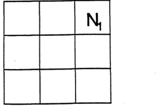
For the reasons discussed above we take a more general approach to this problem. We start with a layout of N elements (gates or switches), which we partition into N/N1 groups of N1 elements each (Fig.
1). All connections internal to a group are made electrically, whereas connections between elements in different groups are made optically. Notice that
N1 = N corresponds to an all electrically connected
system, whereas N1 = 1 corresponds to an all optically
connected system. For given total number of ele-ments N and bit-repetition-rate B we calculate the optimal value of N1 maximizing our optimization
function
r,
which in general can be a function of signal delay, total system size, and power consump-tion. We are interested mostly in high-performance systems for which system size and power dissipation are only secondary considerations, the primary consid-eration being minimization of signal delay. We also consider optimization functions putting a greater emphasis on cost of size and power.In Section 2 we describe the models and the important variables used in this study. Section 3 outlines the general procedure, and Section 4 pro-vides some remarks on the numerical examples. The major results of this paper are derived in Section 5 (two-dimensional systems), Section 6 (the effect of the cost of system size being taken into account),
Section 7 (the effect of repeaters being used), and Section 8 (three-dimensional systems); our predomi-nantly analytical treatment is illustrated by numeri-cal examples. Section 9 provides discussion and conclusions.
Results of this study were first presented in Ref. 20 and subsequently in Ref. 21. This paper is a simpli-fied and condensed version of the more elaborate
Fig. 1. Partitioning a system of N elements into N/N1 groups of
N1elements each (N/N, = 9).
analysis presented in Ref. 21. Unlike that study, in which the aim was a more general formulation, here we employ the simplest treatment that still leads to the same conclusions, so that our exposition is more transparent and instructive. The reader is referred to that study for extensions and generalizations.
Our analysis involves several approximations. Some are made to maintain analytic simplicity and transparency, others are made to maintain generality. In order to be more exact, we would have to introduce several new parameters and make many arbitrary assumptions. Dependent on the details of the de-sign, additional factors or terms would have to be included in our expressions. We avoided doing so when the error incurred does not exceed a factor of the order of unity, since we believe that there is no point in trying to specify and to keep track of such factors in this type of (general) analysis.
2. Model Description
A. Wireability Limitations and Connectivity Model
The spacing between the elements (switches and gates) of a computing system must be large enough to permit sufficient space for the interconnections to pass between them. Systems employing longer con-nections require greater interelement spacing than systems employing shorter connections. We speak of systems employing greater fractions of longer connections as being highly connected. Here we present a model that enables us to quantify the connectivity of computer circuits to first order, and we can predict the interelement spacing necessary to ensure that there is enough space for implementing the desired pattern of connections. This is not the only such model possible, nor one that is suited for every possible situation. However, there are strong rational and empirical foundations for adopting it, in addition to its being well suited for the type of analysis we intend to pursue.2 2"14 2'
For the purpose of this study a processing system is a collection of N given similar elements connected to each other according to a prespecified graph. A list of symbols is provided as Table 1. k denotes the number of connections (graph edges) per element (for simplicity we are considering pairwise connections only; the extension to fan-in and fan-out is not considered); thus there is a total of kN connections. Within a factor of 2, we may also interpret kN as the
total number of input-output ports.
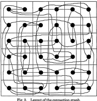
dd denotes thelinear extent of the elements. Let the N >> 1 elements comprising our system be laid out on an e (equal to two or three) -dimensional Cartesian grid of as yet unspecified lattice constant d with
N'/e
ele-ments along each dimension (Fig. 2). Figure 3 de-picts a hierarchical partitioning of this array of cells. During the course of our analyses it is necessary to specify the following quantities in order to obtain explicit results:(1) The average connection length T of the layout (in grid units).
Table 1. List of Symbols
A Cross-sectional area associated with each physical line. Y Area (base area) of two (three) -dimensional system.
B Bit-repetition rate along each edge of connection graph.
d Linear extent of a unit cell, identical to interelement spacing.
dd Linear extent of an element.
dm Center-to-center spacing of modules.
dtr Linear extent of an optical transducer.
di Linear extent of a module of N elements.
e Euclidean dimension of layout space.
E Energy associated with each transmitted bit of infor-mation.
f Identical to W/X for optical systems.
k Number of graph edges (connections) per element.
/ Length of a line in real units.
.2 Linear extent of the system.
M Number of interconnection layers.
N Number of elements.
Ni Number of elements in each module. p Rent exponent of layout.
Se Total power dissipation.
Q Maximum amount of power we can remove per area.
r Length of a line in grid units. S Inverse of worst-case signal delay.
Td Response time of devices.
Tr Minimum pulse-repetition interval along a line. V Nominal voltage level.
W Transverse linear extent associated with each physical line.
Wmin Minimum manufacturable linewidth.
a Defined in Eq. (9). 13 Defined in Eq. (12). y Defined in Eq. (10). r Optimization function.
K Coefficient for average connection length.
X Optical wavelength.
X Worst-case signal delay.
seTM~~~-~771-
;aiw[I
Fig. 2. Layout of the connection graph.
gives the expected number of connections in our system with lengths lying in the interval [ro, r + Ar] and approximately satisfies
f
Ng(r)dr =kN.
{Thus k-lg(r) may be interpreted as a probabilitydistribution defined over [1, rmaj } rmax 1 denotes
the longest connection length (in grid units), assumed to be of the order of the linear extent of the system. We take rma = Nl/e without concerning ourselves with precise geometrical factors. (As we have al-ready discussed, there seems to be little gained by our trying to specify and carry around factors such as
V.)
The parameterp, known as the Rent exponent, is our measure of connectivity. Systems with large Rent exponents have a large fraction of longer connections. (2) The longest connection length rma (in gridunits).
(3) The number of connections P(N') emanating from a group of N' elements in the partitioning of
Fig. 3.
All of the above quantities can be specified by postula-tion of the distribupostula-tion of line lengths for our system. (The terms line, connection, and graph edge are used interchangeably.) Obviously we cannot hope to ac-count for all possible connection patterns. Rather we seek a simple analytic distribution function with a few variable parameters, which we hope is representa-tive of the wireability requirements of typical circuits. Provided the parameter 0 p < 1 (to be discussed shortly) is not too close to unity (say p < 0.9), we assume the line-length distribution g(r) to be of the form2 2-24 (for an expression valid for all values of 0
<
p < 1, see Ref. 21)
g(r)
=ke(1
-p)re(Pl)l
where r denotes distances in terms of grid spacing so that physical distances are given by/= rd. Ng(ro)Ar
11~~~
I
I
- - -
-Fig. 3. Binary hierarchical partitioning of the array of cells. A group at the ith level has N' = N/4i cells.
2970 APPLIED OPTICS / Vol. 33, No. 14 / 10 May 1994
Whenp is small, it is more likely for a connection to be made to close-by rather than to distant elements.
Since e(p - 1) - 1 < 0, we observe that Eq. (1) is
simply an inverse power law. Gien an empirical line-length distribution, one may attempt to fit Eq. (1) by suitably choosing p. If this is not possible, some other functional form must be employed. We dis-cuss our preference for this type of distribution in
Ref. 22.
The average connection length r = k-1 frma rg(r)dr
can be calculated as
r
K(p,e)NP
(e)/e
(2)
K(p,
e) 1 -e(l -p)
(3)
for p > (e - 1)/e (which is the only case to be discussed here; locally connected systems with smaller values of p usually do not suffer from interconnect limitations and thus are not interesting from the viewpoint of this paper). Equation (3) is the defini-tion of the coefficient K appearing in relation (2).
In order to ensure that there is enough space between the elements for the connections, we need to set the interelement spacing d large enough to permit the passage of at least approximately kr connections through each elementary cell.25 26 For instance, for an e = 2 -dimensional system, if the width of each connection is W, then the minimum value of d would be krW. The linear extent 2 of the system would then be at least Y = N1/2krW = k KNPW, where in the
last step we used relation (2). Of course, the linear extent must also be at least 2 = N1/2dd. Thus the system linear extent would be given by the greater of the right-hand sides of these equations. If the tech-nology permits M connection layers, this can be written as
y = max(N1/2dd, kKNPW/M). (4) For larger values of N the second term dominates since we are restricting ourselves to the case p < 1/2. The same analysis can be repeated for an e = 3 -dimensional system, resulting in
2 = max[N1/3dd, (kKNP)'/2W]. (5)
Our line-length distribution is consistent with the following expression for the number of connections
P(N') emanating from a group of N' elements2 3 24:
P(N')
= kN'P.(6)
Equation (6), historically known as Rent's rule, is valid provided N' is not very close to N (say, N' <
N/4). This equation implies that the number of connections emanating from the boundaries of a group increases sublinearly with the number of ele-ments N' in the group. Larger values of p
corre-spond to a stronger increase with N'.
The reader is referred to Refs. 14, 21, and 22 for
discussion, elaboration, and justification of this model, as well as an extensive list of references. The essen-tial assumption we make is that we can speak mean-ingfully about a distribution of line lengths for our system. Readers who prefer some other form for the function g(r) may easily modify the results of this paper by using appropriate expressions for r, rmar and
P(N') corresponding to their particular choice of g(r).
The qualitative results of this paper (for instance, that a particular quantity increases with increasing connectivity) remain applicable regardless of how one chooses to model or measure connectivity.
B. Heat-Removal Model
The interelement spacing of a computing system must also be large enough that we can successfully remove the dissipated power. Packing the elements too densely may result in unacceptable temperature rises and destruction of the system. For systems in which the power-dissipating elements are confined to a planar surface we assume that there is an upper limit to the amount of power we can remove per unit area, denoted by Q (W/m2). Thus power dissipation
! 9 and linear extent Y of a square system must
satisfy
Q2
2 2 3.For systems in which the power-dissipating ele-ments are distributed throughout a volume, one can again quantify our heat-removal capability by the
quantity Q, this time interpreted as the amount of
power we can remove per unit cross-sectional area of the volume.1'27 We do not require this result, how-ever.
C. System Characterization
In this study we assume that the performance of our systems can be characterized in terms of those param-eters: the number of elements, N, the bit-repetition rate, B, along each edge of the connection graph, and the inverse signal delay, S = 1/T. Although it would certainly be desirable, it is not possible to arbitrarily increase S, B, and N simultaneously because of physical limitations. For simplicity the rate B (bits/s) at which information is piped through the connec-tions is assumed to be the same for all connecconnec-tions. Likewise, signal delay T is taken as the worst case
(maximum) over all connections, as is appropriate for synchronous systems.
D. Interconnection Models
We characterize physical interconnection media in terms of the following parameters: (i) Interconnec-tion length A. (ii) Cross-secInterconnec-tional area A or trans-verse linear extent W (where A = W2). These param-eters define packing density for three- and two-dimensional systems, respectively, and thus include any necessary line-to-line separations. (iii) Signal delay T. (iv) Minimum pulse-repetition interval Tr, i.e., the minimum time interval between consecutive bits on the line. (v) The energy per transmitted bit, E. (Subscripts are used whenever necessary to clarify whether one of the above parameters is associated
with an optical or a normally conducting line, e.g., E0
orEs.)
Td denotes the response time of the devices (gates and optical transducers). Of course in general the value of Td may be different for each of these, but for
simplicity we assume that the rate at which the gates
may be switched and the optical sources modulated are more or less the same. In almost all cases, minimum bit-repetition interval T cannot be less than Td. This limits the rate B at which we can pipe information through each connection. Thus we assume that B is always specified so as to satisfy B <
1/Td. (B can be increased beyond /Td by use of several physical channels in parallel to establish each connection or by employment of wavelength-division multiplexing. Both complications, discussed in Ref.
14, are avoided in this paper.)
In the following sections we present models for optical and normally conducting interconnections in their simplest possible form. Detailed derivations and elaborations may be found in Refs. 14 and 21.
1. Optical Interconnections
The cross-sectional area per independent spatial chan-nel is taken to be proportional to the wavelength squared: A = W2 = (fX)2, where the constant f can
be as small as 1 for a diffraction-limited system but may be much larger in practice. In the context of a two-dimensional integrated optics system this simply means that waveguides can be packed at a transverse density of one every W = f. We have argued elsewhere that this is a suitable model for three-dimensional systems as well,2 8'2 9'21 at least from a fundamental perspective. Of course, if one is con-fronted with a particular optical architecture, as in Refs. 30 and 16, one can determine the space required for communication directly without resorting to pa-rameter W. The analyses presented in this paper can be easily adapted to such architectures.
The signal delay is taken to be the greater of the speed-of-light delay and the device response time:
X = max(//c, Td). Since the effects of dispersion and attenuation can be made small for the length scales in consideration, minimum pulse-repetition interval
Tr Td and energy per transmitted bit E are assumed to be constants. The value of E0 is
deter-mined largely by the properties of the light
source/modulator and the detector.9"5
As a simple example, let us derive the signal delay for a wireability-limited (that is, the interelement spacing is set by wireability limitations) two-dimen-sional integrated optics system with very small
ele-ments (dd negligible), very fast devices (Td negligible),
and only one connection layer. Using /ma. = Y and
Eq. (4), we obtain14
T = (max/C =
'/c
= k KNPfX/c, (7)and S = 1/T. If the system is heat-removal limited, QY2 must exceed the total power dissipation 9 =
kNEoB (since there are kN connections dissipating
EoB each); thus the signal delay is given by
= max/C =
'/c
= (kNE.B/Q)'/ 2/c.
(8)2. Normally Conducting Interconnections
Shorter normally conducting interconnections can be left unterminated, whereas longer ones must be terminated. However, detailed analysis permitting termination of conducting lines shows that it is optimal to start employing optical interconnections at lengths for which it is not yet necessary to terminate lines.21 Thus it makes little if any difference in our
results if we restrict our attention to unterminated
lines only. This permits considerable simplification. The relationship between the rise-time, the length, and the cross-sectional parameters of an untermi-nated RC line is given by Refs. 14 and 21
TRC = CL w
(9)
where a is a constant proportional to the resistivity of the conductor and the permittivity of the dielectric isolating the conductor from the ground plane. It is assumed that the optimal ratios between all trans-verse dimensions of the line are maintained for different values of W. (A line with width comparable to its height is close to optimal. Increasing the width increases capacitance and reduces packing density. Increasing the height increases fringe effects, again forcing a reduction in packing density, without im-proving the capacitance considerably.9 4) Although we refer the reader to the above references for a derivation, it is easy to convince oneself that this equation makes sense. TRC is proportional to RC/2
,
where R and C are the resistance and the capacitance of the line per unit length. C is proportional to the ratio of the width of the line to the height of the dielectric; thus it is not affected by scaling of W. On the other hand, R is inversely proportional to both the width of the line and the height of the conductor; thus R cX 1/W2. Of course, no matter how small the rise time, the signal delay cannot be less than device delay Td, so = max(rRc, Td). The energy per trans-mitted bit is given by
(10)
where y is a constant proportional to the permittivity of the dielectric and the square of the nominal voltage, V. The energy is proportional to C/V2, and since C is not affected by scaling W, the above equation is justified.
For simplicity we assume that all lines in a given system are of the same width W. (This assumption is relaxed in Ref. 14.)
Again, as an example, let us derive the signal delay for a two-dimensional system with very small ele-ments and very fast devices. Using ma. = Y and Eq.
(4), we find14
T = CL/2a /W2 = I(kiNP/M)2. (11) 2972 APPLIED OPTICS / Vol. 33, No. 14 / 10 May 1994
For an unterminated RC line the signal delay is also the minimum bit-repetition interval, which deter-mines the maximum bit-repetition rate. Thus B <
S= 1/T.
The above result is scale invariant'4; i.e., it does not depend on W. If technology enables us to manufac-ture very fine lines, heat-removal requirements will determine how much we can scale down the system and thus its minimum linear extent, but this will have no effect on the delay (provided the scale of the system does not have to be so large that the lines become propagation limited14). To find the heat-removal-limited linear extent of the system, first note that the dissipation associated with each cell is
,yk/B = yk-dB [obtained by Eq. (10) and because
there are k connections per cell with average length
= d, switched at a rate B]. Using relation (2) and
requiring that the power dissipation per cell not exceed Qd2, we can show that the system linear
extent 2
= N1/2d = YkKNPB/Q.3. Repeatered
Normally Conducting
Interconnections
The inhibitive square-law behavior of normally con-ducting lines may be alleviated with the use of repeater structures. Bakoglu and Meindl derived the optimal configurations of such structures.3' The delay along such a line is given by Trep oc (RoCoRC12)112 where RoCo denotes the intrinsic delay of the repeat-ers. Following scaling arguments similar to those with ordinary normal conductors, we may write this in the form
rep= 3W (12)
where is proportional to (RoCo)'/2 as well as the square roots of the conductor resistivity and the dielectric permittivity. The effect of repeaters being used on the energy per transmitted bit can be ignored
so that Eq. (10) is still valid.
Following the derivation of earlier results, one can show that the signal delay for a two-dimensional repeatered system with very small elements and very
fast devices is given by'4
=
pe'max/W
= (kKNP/M). (13)The effect of heat-removal requirements is similar to that in the unrepeatered case.
4. Superconducting Interconnections
Superconducting interconnections are not treated in this paper. Let it suffice to say that superconductors lead to similar results as optical interconnections, both analytically and numerically.'4 However, there is one exception: The energy per transmitted bit can be made much smaller than with optical interconnec-tions, especially at lower temperatures; thus they may be advantageous in heat-removal-limited systems. On the other hand they suffer from termination
problems, and the prospects for three-dimensional circuits are no better than for normal conductors.
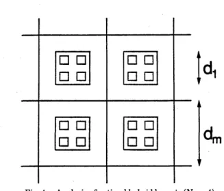
3. Outline of the Analysis
Now we actually outline the steps of our analysis (Fig. 4). The linear extent di of an electrically connected group of N, elements must be large enough to do the
following:
(1) Accommodate N, elements.
(2) Accommodate the electrical wires connecting them.
(3) Accommodate kNP optical transducers [Eq. (6)].
(4) Satisfy heat-removal requirements.
Then dim the intergroup spacing of the electrically connected groups (also referred to as modules) must be large enough to do the following:
(1) Accommodate
di (i.e., d. 2 di).
(2) Accommodate the optical channels connecting the groups.
(3) Satisfy any additional heat-removal require-ments.
Note that the N elements (switches and gates) are no longer uniformly laid out as in Fig. 2 but are clustered into modules. This enables considerable energy sav-ings since the electrical wires can be made much shorter.
On the basis of these considerations we can write expressions for the signal delay (which is taken as the worst case over all connections), the system size, and the power dissipation as functions of N, B, and N1. Then we can pick the value of N, maximizing our figure-of-merit function.
We carried out this analysis for a variety of layout constraints, combinations of media, and physical parameters. It is not possible (and perhaps not useful) for us to reproduce all of our results. Rather, we try to present representative examples chosen for their illustrative qualities and qualitatively discuss
LPJ
[pJ
?d,
dm
Fig. 4. Analysis of optimal hybrid layouts (N1 = 4).
several general conclusions deduced from the study of a large number of cases.
Although not attempted in this paper, systems with three or more hierarchical levels can also be ana-lyzed.2' This would permit systems involving nor-mal conductors, superconductors, and optics all to-gether.2' It would also enable the different parameters of electrical interconnections at different levels (such as on-chip and multichip substrates) to be taken into account.
4. Regarding Numerical Examples
In our numerical examples we try to look into the future and to select reasonably optimistic parameters for each interconnection media. We also consider the effects of degradation of the optical parameters from what seems to be their best possible values, as it is not yet a mature technology.
We assume 10-GHz devices, i.e., Td = 0.1 ns. We
permit a maximum of M = 10 conducting connection layers but only one optical connection layer for two-dimensional layouts. We assume a nominal voltage
level of V = 1 V and room-temperature aluminum
conductivity. The parameters a, 13, and y are taken
as 1.5 x 10⁻¹⁷ s, 3.9 x 10⁻¹⁴ s, and 6.9 x 10⁻¹ J/m,
respectively.2' These values roughly correspond to the best possible at room temperature, with 10-GHz repeaters. Since our analysis is approximate, these numbers can also be rounded to the nearest order of magnitude; however, we use them as they are so that consistency with Ref. 21 is maintained. We permit a maximum power dissipation per unit area of Q = 10 W/cm2. The minimum manufacturable value of W for conducting interconnections is taken as Wmi = 0.2 pum. Element size dd is assumed to be ten times this value. (This implies that our elements are of the simplest type, such as logic gates.) We assume there to be k = 5 connections per element. We take = 1 m as the optical wavelength. The optical transducers are assumed to be dtr = 5 pm in diameter. We assume the best possible optical communication energy to be E0 = 1 pJ, but we also consider
degrada-tion of this value by a factor of 100. Likewise, we consider near-diffraction-limited operation (f = 2),
but we also consider degradation of this by a factor of as much as 100 (f = 200). We consider two different
values of the Rent exponent, p = 0.6 and p = 0.8, to observe the effects of connectivity on the results. The values chosen above for W,,, dd, and dtr, which seem realizable in the near future, are already small enough that in most cases, totally ignoring the effects of these parameters will have little or no effect on our
results.
Our primary objective is minimization of signal delay. As a secondary objective we try to minimize total power dissipation. In other words we try to minimize signal delay as much as possible, and only then, to the extent possible without making any sacrifice from the minimum signal delay, do we try to minimize power dissipation. This approach empha-sizes performance, and cost is minimized only if this
can be achieved without performance being sacrificed. Analytically this can be realized by maximization of
S
F
= -) e -> 0. (14)Other figures of merit emphasizing cost are also discussed.
Computationally, we chose E = 10-10. We
ob-served that choosing values as large as 10-5 or as small as 10-12 makes no difference. Values larger than 10-5 start changing the results in favor of systems exhibiting somewhat larger signal delay but less power dissipation. Values lower than 10-12
start causing numerical problems.
5. Two-Dimensional Systems
In this section we consider fully two-dimensional systems, i.e., systems that are confined to a two-dimensional surface, including optical paths. One implementation of such a system may involve a two-dimensional array of VLSI chips with optical transducers located on a topmost layer or on dedi-cated islands. The optical imaging system may be a glass waveguide overlay or the folded multifacet architecture described in Ref. 32.
A. Analysis
We refer to Fig. 4. We assume that there are k connections per element. Some of these connections are made to elements in the same module and are implemented with normal conductors. Other connec-tions are made to elements in other modules. One can establish such connections optically by tying
optical transducers at the to-be-connected terminals
and by guiding the light emanated from the source terminal to the target terminal with some type of optical imaging system. It matters little whether the transducers are on a separate layer or side by side with the electrical wiring [since max(x, y) x + y
within a factor of 2]. The intergroup spacing dm may have to be larger than d because of the space necessary to accommodate the optical channels. Again, it makes little difference whether we assume that the optical channels are on a separate layer or that they compete for the same space with the modules. As discussed earlier, there is little purpose in specifying such details, as they ultimately change the results by factors such as 2,
V4,
etc. If one is confronted with a particular system for which such details are specified, such factors can be readily introduced in order to obtain more accurate results.Remember that our purpose is to determine, for every N and B < 1/Td, the value of N, maximizing our figure-of-merit function. We can immediately set an upper bound on N, since we know that the maximum bit-repetition rate, B, is a decreasing func-tion of the number of electrically connected elements
[Eq. (11) and the following remarks]. We can solve
for N, from Eq. (11) (rewritten for a module with N1,
rather than N elements, and since B < 1/- for
unterminated conducting lines) as
N, < (M/kK)'/P(1/aB)/2P. (15) The right-hand side of this inequality is the largest value of N compatible with given B. We denote
this value of N, as N
. For given B, N, must be
chosen to lie between 1 and N 1 .
Ignoring heat-removal requirements for the
moment, we see that the linear extent of each module d, must satisfy
d,
2max[N]/
2dd,
kKNPWmin/M, (kNP)1/2dtr, kNp(fX)].
(16)
The first term is trivial. d must be at least large enough that the module can accommodate N1/2 x N'/2 elements of linear extent dd each. The second term is simply the smallest module linear extent that still provides enough room for routing the electrical connections at the minimum manufacturable line-width Wnin. These two terms correspond to Eq. (4). The third term accounts for the fact that the module must be at least large enough to accommodate kNP transducers of linear extent dtr, since this many connections are made to elements in other modules [according to Rent's rule, Eq. (6)]. The final term accounts for the fact that the linear extent of the module must be large enough to permit the passage of
kNP optical channels through it; otherwise, the
chan-nels emanating from the transducers would not be able to get out of the boundaries of the module. (Such a problem does not arise if out-of-plane optical communication is permitted.) The values of dd and
Wmin/M
are often small enough that the first twoterms can be ignored. Technological improvements will further decrease dd and Wmin and increase M so that it is unlikely for these terms to determine dj.
Also, since dtr need not be much larger than fX (i.e.,
the transducers need not be much larger than the transverse extent allocated for each channel), the third term will often be shadowed by the fourth. Thus in most cases we will be left with the single term
d, 2 kN (fX).
Heat-removal considerations will require that
Qd' > (electrical dissipation plus optical dissipation).
(17)
First, let us calculate the electrical dissipation. We can find the total connection length by multiplying the total number of connections kN1 by the average
connection length = d (where, as before, d is the interelement spacing of the elements). Then, with Eq. (10), the total energy involved in one cycle is ,ykN1l and the power dissipation is ykNI/B. Using relation (2) and also d, = N1/2d, we find the total
electrical power dissipation to be ykrNPBdl. The optical power dissipation per module is simply the number of optical connections per module times the
power dissipation EB per connection, giving
kNP'EB. Using these results, simplifying inequality
(17) with x + y max(x, y), and solving for dj, we obtain
d1 2 max [(kNzE 0B)'/2
ykKNPIB]
Combining this with d, 2 kNP(fX), we obtain the minimum value of d, as
r {kN~l~oB1/2
-ykKNlBl
d
=maxIkN)(fX),
Q )
Q
j* (19)
The minimum value of the intermodule separation, dm, is then given by
d = max[dj, kKN(N/N)P-1/ 2(fX)], (20)
where we assume only one optical connection layer. Apart from being large enough to accommodate the module, the intermodule spacing must be large enough to permit the passage of at least kNPK(N/N,)P-1/ 2 optical- channels. (Remember that the spacing be-tween elementary cells had to be large enough to permit the passage of at least kr = kuNPl- /2 connec-tions. Now replace k -> kNP and N1 -- N/N1, since
now instead of N, elements with k connections each, we have N/N, modules with kNP connections each.)
The system signal delay is finally given as the maximum over all connections:
= max[(N/N1)1/2d./c, ao(kK/M)2N2P, Td). (21)
The first term is the speed-of-light delay along the longest optical connection. The second term is the delay along the longest normally conducting intercon-nection, and the last term accounts for device delay. Employing previous equations, we obtain
T = max[kKNP(fX/c), (N/N1)/2(kNjE.B/C2Q)'/2,
(NIN,)112 (ykK1NPB/cQ), a(kKIM)2N2P, Td] (22)
for the resulting signal delay for a hybrid system. The signal delay for an all-optical system under the same approximations is given by the maximum of the right-hand sides of Eqs. (7) and (8) and Td. For an all-electrical system it is given by the maximum of the right-hand side of Eq. (11) [Eq. (13) with repeaters and Td.] The first term, which is independent of N1,
is also the delay of an all optically connected system of N elements [Eq. (7)]. Thus we conclude that the use
of a hybrid layout cannot reduce the system size and delay below that of a wireability-limited all-optical system.
Since N, < Nmax, the first term in the above equation eventually dominates the others with in-creasing N (remember that our expressions are valid
forp > 1/2). When this is the case, the choice of N, has no effect on the delay. Thus we choose that value resulting in minimum power dissipation. The total power dissipation is expressed as
.9
= (N/N)(kNJE 0 +ykKNldl)B
= (N/N)max(kNPjE 0, ykKNPd,)B. (23)
When d, is given by the first term of Eq. (19), the value of N, minimizing total power dissipation is
given by
NP 1 y(f X)kK -E. (24)(4
For larger values of B either of the two latter terms in Eq. (19) may dominate. Interestingly, whichever of these two terms dominates, it is possible to show that the value of N, minimizing relation (23) is given by the same expression:
NJ = kEoQ (25)
=(-ykK) 2B (5
[Incidentally, we also note that this value of N, minimizes the combined second and third terms of Eq. (22).] We see from this equation that the opti-mal value of N, increases with the optical communica-tion energy and our heat-removal ability and de-creases with the bit-repetition rate and the Rent exponent. It obviously increases with increasing E, as optical communication becomes energetically more expensive. It also increases with increasing Q: if we are able to remove larger amounts of power per unit area, this means that the scale of the electrically connected groups can be reduced, reducing the energy cost of electrical interconnections. On the other hand, increasing B reduces N,, since it results in an increase in power dissipation and d,, making electri-cal interconnections more expensive. N also de-creases with increasing p. Systems with larger p have a larger fraction of longer connections, so it is beneficial to make fewer electrically.
Of course, since we are giving full precedence to minimizing signal delay, keeping the latter terms of Eq. (22) at less than its first term has priority over minimizing power. For instance, so that the fourth term of Eq. (22) does not exceed the first, we must maintain
N,
<(fX/c M
2)
2NP/2
(26)
Thus the optimal value of N, is determined by three considerations. For larger N it is that value which minimizes total power consumption, as given by either of Eqs. (24) or (25), with the restriction that it can never exceed Nma. These two considerations determine the optimal value of N, for large N. The optimal value of N, should also not exceed the
envelope given by inequality (26). This last restric-tion relaxes with increasing N. Notice that the effect of variation ofp on all three of these considerations is the same: larger Rent exponents favor the use of
more optics.
Naturally, it is possible for there to be combina-tions of parameters and variables for which other terms that we neglect dominate. But in most cases the above expressions agree with the calculations of Ref. 21, in which all terms were maintained. Thus they suffice for our purposes.
B. Numerical Examples
Throughout this paper we keep all but three of the physical parameters the same for all examples, as discussed in Section 4. Thus in the following we only specify the values of p, f, and E for each example.
In our first example we consider a system with Rent exponentp = 0.6, optical communication density only
f = 2 times worse than diffraction limited, and an
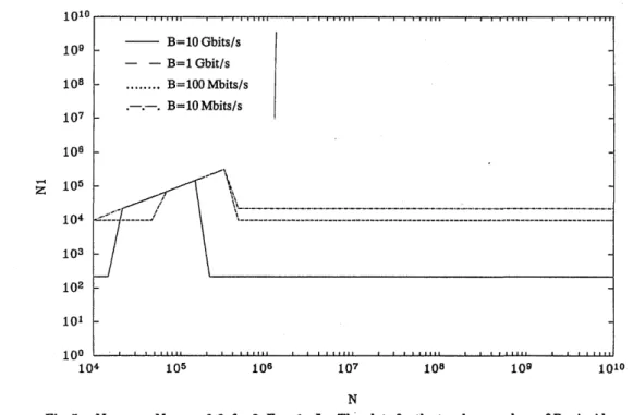
optical communication energy E, = 1 pJ. Figure 5 shows the optimal value of N, as a function of N with
B as a parameter. In all numerical plots we vary N from 104 to 1010. One should keep in mind, however, that the larger values of N in this range may lead to unrealistic system sizes and/or power dissipations for some combinations of the parameters. For the two lower values of B it is optimal to make all connections electrical (i.e., N, = N) until N 2 x 10⁵, after which the optimal value of N, is independent of N and is that value that minimizes total power consumption. For these relatively low values of B the size of each electrically connected group d is given by d =
kNP(fX). Thus the total power dissipation is given
by relation (23) with di = kNP(fX). The value of N, that minimizes power dissipation is given by Eq. (24) and is indeed consistent with that observed in Fig. 5 for the two lowest values of B. For the two larger values of B the latter terms of Eq. (19) dominate so that the optimal value of N, is given by Eq. (25), which indeed predicts the optimum values of N, for the two larger values of B in Fig. 5. [The optimal values of N, for smaller values of N are determined by the competition of the various terms in Eq. (22), until the first term dominates the others, after which N, is given by Eq. (25).]
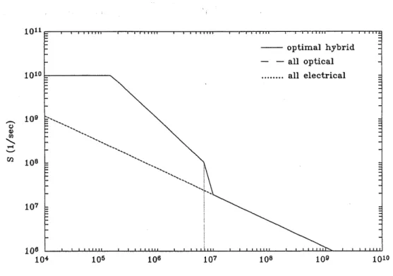
Figure 6 illustrates the resulting dependence of S on N for B = 100 Mbits/s. The solid curve corre-sponds to the optimal choice of N,. The dashed curve corresponds to all connections being made optical and coincides with the solid curve for larger values of N; it is given by
1/S
= . = kKNPfX/c. Thedotted curve, which overlaps with the solid curve initially, corresponds to all connections being made electrical and is given by a(kK/M)2N2P. We cannot
make all connections electrical once N > N, = 7 x
106; thus the dotted curve terminates at this value of
N. After a certain value of N, making all
connec-tions optical is as good as the optimal hybrid
1010 109 108 107 -106 -; 105 -104 103 102 -101 100 _ 104 105 106 107 108 109 1010 N
Fig. 5. N versus N: p = 0.6, f = 2, E0= 1 pJ. The plots for the two lower values of B coincide.
tion in terms of minimization of system size and delay, as discussed previously [following Eq. (22)].
However, making all connections optical results in power dissipation 1 order of magnitude larger than the optimal hybrid combination for the largest value of B and 2 orders of magnitude larger for the smallest value of B. The disparity is greater for smaller values of B because the optimal value of N is larger when B is smaller. In other words the all-optical system (N1= 1) is farther away from the
loll
1010 Q C) _4 C/2 109 108 107 186 10)4 105 106optimum. These considerations have no effect on the resulting system size and signal delay, since two-dimensional systems tend to be wireability rather than heat-removal limited. Another consequence of this is that the resulting values of S for different values of B are identical.
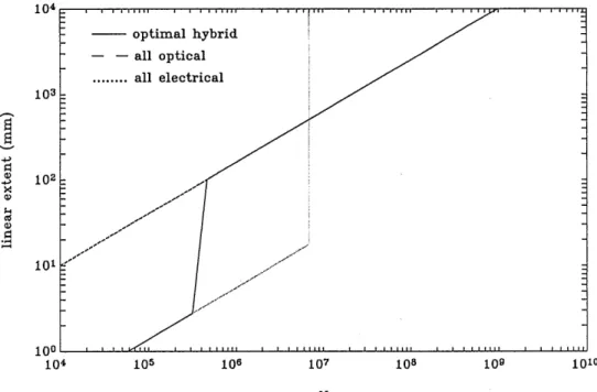
The entrance of optical interconnections after N 2 x 10⁵ elements is accompanied by a drastic increase in system size, as illustrated in Fig. 7. The linear extent of the all-electrical system is given by
107 108 109 1010
N
Fig. 6. S versus N: B = 100 Mbits/s, p = 0.6, f = 2, E0= 1 pJ. The plot for the optimal hybrid case first coincides with that for the
all-electrical case and then with that for the all-optical case.
10 May 1994 / Vol. 33, No. 14 / APPLIED OPTICS 2977 optimal hybrid
- -all optical
.all electrical
105 106 107 108 1 09 1010 N
B = 100 Mbits/s, p = 0.6, f = 2, E0= 1 pJ. The plots for the all-optical and the optimal hybrid cases coincide for
ykIKNPB/Q. Once we start using optical
communica-tion for the longer conneccommunica-tions, they dominate the system area, leading to a linear extent given by
k KNPfX. The curve for S is continuous because the
fast velocity of propagation of optical interconnec-tions compensates for the increase in system size. We can avoid the jump in system size by keeping all connections electrical; however, in this case the value of S is less than that possible with a hybrid system. This is one example of a situation in which the use of
1010 109 -- 0 Gbits/s - -B= 1 Gbit/s 108 ... B=lOOMbits/s 107 .-.-. B=10Mbits/s 106 105 104 103 102 101 100 104 105 106
optics permits performance not possible with normal conductors alone but at a significant penalty in terms of system size.
Let us now explore the effects of degradation of the optical parameters. The optimal value of N, when
f = 50 is plotted in Fig. 8. We observe that it is
beneficial to stick to an all-electrical system (N1 = N)
until N > N1 , after which the entrance of optics is
unavoidable. m7If f is too large, the increase in 2 accompanying the entrance of optics may be
unreason-107 108 109 1010
N
Fig. 8. N, versusN p 0.6,f J 50, o 1 pJ. All plots coincide for the smallest and the largestvalues of N.
2978 APPLIED OPTICS / Vol. 33, No. 14 / 10 May 1994 104 103 102 2) 4-, x 2) Ca 2) Fig. 7. 9 versus N: larger N.
Jole
100 104ably large; thus increasing N beyond N, while we maintain the given value of B may not be feasible.) Once this occurs, module size d is limited by the term
kNP(fX) for all values of B. The resulting large
value of d, makes electrical connections expensive, leading to a small optimal value of N,, as given by Eq. (24). Notice that although increasing f leads to an overall degradation in performance and cost, it results in greater use of optics when N > N1m
Figure 9 illustrates the resulting dependence of S on N. Notice that in this case, unlike in the previous example, a sudden drop in S is observed. This is because we are forced to use optical interconnections prematurely so as to maintain the given value of B, before the value of S for an all-electrical system falls below that for an all-optical system (as was the case in
Fig. 6).
In other words, when f > 10 or so, we have a region in S-B-N space in which a small increase in N or B is
accompanied by a large increase in system size and a large decrease in S. This behavior may have algorith-mic implications.'4 Among several algorithms de-signed to solve a given problem it may be preferable to employ those requiring relatively smaller values of N and/or B, if possible, since even small increases in these parameters require a large sacrifice in terms of
S. For instance, if we are trying to maximize a
figure-of-merit function of the form SxBY, where x, y > 0 and x is not much smaller than y, it is likely that we will settle for an operating point not involving any optical interconnections.
In conclusion, if the use of optics is to be worth-while for two-dimensional systems, it is of paramount importance to bring f as close as possible to unity.
1011-1010 C) 2) 1-I C/2 109 108 107 106 10 4 105 106
The folded multifacet architecture described in Ref. 32 was devised to meet this requirement.
Now we discuss the effects of an increase in the optical communication energy hundredfold (Fig. 10). For large N the optimal value of N, is seen to hit Nm. For smaller N we observe the envelope
N1 c N'!2 given by inequality (26). Despite the fact
that increasing the optical energy results in a drastic shift in N,, it has no effect on the resulting value of S, which is still as given in Fig. 6. This is because the system is still wireability limited. (An exception occurs for the largest values of B, for which the system may be heat-removal limited up to a certain value of N.)
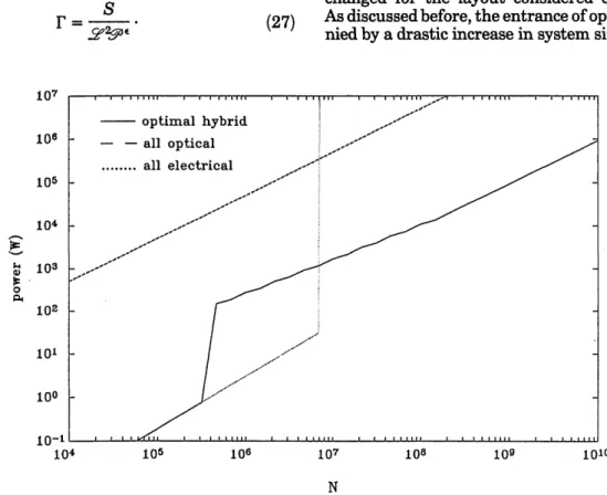
Of course, now the total power dissipation is much larger, and the discrepancy between the optimal system and the all-optical system in this respect is even greater than before. The entrance of optics results in a large increase in total power dissipation (Fig. 11). The all-optical and the all-electrical sys-tem power dissipations are given by kNEoB and
(ykKNPB)2/Q, respectively. The total power
dissipa-tion for the optimal hybrid case for larger N is given
byNkNP'E
0B
withN,
5
x 106.
Let us now consider that p is increased to 0.8 (Fig. 12). The downward shift in the optimal values of N, is easily explained by the changes in the values of N, Once again the envelope given by in-equality (26) is observed.
6. Cost-Based Optimization
Until now we have concentrated on the optimization function given by Eq. (14), which gave full precedence to minimizing signal delay and only secondarily tried
optimal hybrid
- - all optical
... electrical .all
107 108 1 0g 1010
N
Fig. 9. S versus N: B = 100 Mbits/s, p = 0.6, f = 50, E0 = 1 pJ. The plot for the optimal hybrid case first coincides with that for the
all-electrical case and then with that for the all-optical case.
10 May 1994 / Vol. 33, No. 14 / APPLIED OPTICS 2979
105 *106 107 108 N
Fig. 10. N, versus N: p = 0.6, f= 2, E0 = 100 pJ.
to minimize power dissipation. The cost of system size was not accounted for at all. Now we consider another example optimization function, which ac-counts for the cost of system size.
A. Analysis
We consider dividing Eq. (14) by the system area y2:
1' 107 106 105 104 2) 0 Pk 103 102 10 ' 10° 10-1 _ 104
S
(27) 10S 106Of course, it is always possible to employ more complicated functions if desired, depending on the relative importance we attach to speed, system size, and power cost.
B. Numerical Examples
Figure 13 shows how the optimal values of N are changed for the layout considered earlier (Fig. 5). As discussed before, the entrance of optics is accompa-nied by a drastic increase in system size. Thus with
107 108 109 1010
N
Fig. 11. .iA versus N: B = 10OMbits/s,p = 0.6,f= 2,E0= lOOpJ.
2980 APPLIED OPTICS / Vol. 33, No. 14 / 10 May 1994 B=10 Gbits/s - - B=1 Gbit/s ... B=100 Mbits/s B=10 Mbits/s 109 108 107 106 z 105 104 103 102 101 100 104 109 1010 optimal hybrid - - all optical -.. -all electrical .1 ... ... . .... . .. . ... . ... .I... - - --- --- --- -- -- -- -- -- -- -- -- -- -- -l -l -l -l I I l I I I l l 1 I I l I I I .. l l l l l l I I ... . . . I ... . " . . . , , .... . . I I .... , 'I-I11 I I I I I I I I I . .. , I . I I .
105 ' 106 107 108 109 1010 N
Fig. 12. N, versus N: p = 0.8, f = 2, E0= 100 pJ.
our new figure of merit it is beneficial to stick to an all-electrical system until larger values of N despite the fact that the resulting signal delay will be worse than that possible with a hybrid system. However, once N tends to exceed N1 , the entrance of optics is
unavoidable. Once opticaninterconnections are en-tered, the steep increase in system size is observed.
For N > N
,a the optimal values of N, are
1 identical to those in Fig. 5.One other possible figure-of-merit function that we do not deal with here is given by F = Sf9, which is
1010 . I I . ... 109 B=lO Gbits/s -
-B=l
Gbit/s
108 ... B=lOOMbits/s B=lOMbits/s 107 108 10' 104 ---103 102 101 100 104 105 108discussed in Ref. 21. The general conclusion is that accounting for the cost of system size and power dissipation results in all-electrical systems being pre-ferred until very large numbers of elements.
7. Effect of Using Repeaters A. Analysis
There is no maximum value of N1 for given B when
repeaters are used; thus there is no analog of inequal-ity (15). The linear extent of each module must
107 108 109 1010
N
Fig. 13. N, versus N (cost-based optimization): p = 0.6, f = 2, E0= 1 pJ.
10 May 1994 / Vol. 33, No. 14 / APPLIED OPTICS 2981
II 109 108 107 108 B=10 Gbits/s - - B=l Gbit/s . ... B =lOMbits/s B=lOMbits/s - 105 104 103 102 101 100 -104 --- -'.1. - ---ntn v
again satisfy Eq. (19), and the intermodule separation
dm is calculated similarly. Finally the system signal
delay is given by
Xr = max[(N/N1)1"2d/c, P(kK/M)NP', Td]. (28) The total power dissipation is again given by relation (23), and Eqs. (24) and (25) are still applicable. Again, on the basis of arguments similar to those leading to inequality (26), we must ensure that
P(kK/M)Np < kKNP(fX/c).
B. Numerical Examples
Comparing Eqs. (7) and (13), we observe that the relations between S = 1/v and N for repeatered and optical layouts are identical in form and differ only by the numerical factors (fX/c) versus (/M). Optical interconnections have larger linewidths and faster propagation velocity. Repeatered interconnections can (and must) be scaled down to smaller linewidths but have a slower propagation velocity. Let us first consider a system with optical communication den-sityf = 50 times worse than diffraction limited and an optical communication energy of E0 = 1 pJ. The
same results are obtained whetherp = 0.6 orp = 0.8. (For these parameters an all-repeatered layout re-sults in signal delay more than 40 times less than that possible with an all-optical layout). We find that an all-electrical system (N1 = N) is best for the range of
N and B in consideration (Fig. 14). What essentially
happens is that with 10-GHz devices, repeaters per-mit fast propagation. Much smaller linewidths and ten connection layers result in much smaller system size, more than making up for the deficiency com-pared with the speed of light.
It is also interesting to note that no optical commu-nication is used even when the system size exceeds a
14 109 108 107 106 1-4 Z 105 104 103 102 101 10 L 104
centimeter, which is the breakeven length for energy for this choice of parameters. This illustrates the inadequacy of breakeven-length approaches. A sub-micrometer repeatered line cannot be replaced with anf 50 optical line even though the latter may have a smaller communication energy. (Of course, for large N the total power dissipation for the all-repeatered system will be greater than that possible with a hybrid system. Remember, however, that our original figure-of-merit function gives full priority to minimizing signal delay.)
Now, let us assume the value of f is reduced to 2, which we are assuming to be its best possible value. In this case the discrepancy between the use of all repeaters and all optics in terms of signal delay is reduced to less than a factor of 2.
(An exception may occur for the largest values of B for which the system tends to be heat-removal limited. Then, the heat-removal-limited all-repeatered system may result in signal delay greater than that given by the wireability-limited Eq. (13). However, the dem-onstration of this would require consideration of effects not taken into account in this paper and would greatly complicate our analysis; thus we satisfy our-selves by referring the reader to Ref. 21.)
Apart from such cases, when f 2, the signal delay of an optical system is close to that of an all-repeatered system [i.e., Eqs. (7) and (13) are numeri-cally close. This does not mean, however, that we can use optics or repeaters interchangeably for the individual connections in the same system because of scale incompatibility.] The all-repeatered system has much smaller area. Whenp = 0.6, the power dissipa-tion of the all-repeatered system lies quite below that of the all-optical system for the range ofNin consider-ation (although it grows faster with increasing N).
10S 106 107 108 1010
Fig. 14. N versus N (repeaters):
N
p = 0.6 orp = 0.8, f = 50, E =1 pJ. The plots for all values of B coincide.
Thus unless B is very large so that the system is heat-removal limited (as discussed above), an all-repeatered system would be preferred. When p = 0.8, the power dissipation for the all-repeatered case grows faster so that hybridization according to Eqs. (24) and (25) may be beneficial, if minimizing power dissipation is considered to be more important than minimizing system size.
In conclusion, the only situations in which it is desirable to use optics is either when B is very large so that the system is heat-removal limited or when
f 2,p is large and we give priority to minimizing the cost of power over the cost of system size. In practice it is relatively difficult to achieve f 2 imaging. Furthermore, a larger number of conduct-ing connection layers and faster devices may become possible in the near future (the latter of which will reduce the value of
13).
Thus it seems that as long as the optical communication paths are constrained to the plane, optics may have limited usefulness.8. Three-Dimensional Systems
In this section we consider systems in which the modules are still confined to a plane, as in Fig. 4, but the optical communication paths are permitted to leave the plane. Such a system would most likely employ some type of free-space interconnection archi-tecture.
Various other configurations are also possible. For instance, the modules may be arrayed through-out the volume of the system instead of being con-fined to the plane.2 9 The N electrically interconnected elements constituting each module may be arrayed in a three-dimensional lattice, if such a cubic chip can be manufactured. Such alternatives have been considered in Ref. 21. The general
conclu-1010 109 108 107 106
z
105 1U V- 103 102 -101 100 104 i05 106 107sion is that such choices have little or no effect on the optimal value of N1 and the resulting performance
and cost of the system.
Why is this so? Utilizing a volume for the estab-lishment of the interconnections relaxes wireability requirements greatly, whereas it hardly has any effect on heat-removal requirements. (In Refs. 21 and 27 we show that the requirement Q22 .9
holds regardless of whether the system is two or three dimensional.) Thus in three-dimensional systems, heat removal becomes the dominant issue.3 3'2 7'2 As a result, the particular choice of architecture, which essentially has to do with wireability requirements, has little or no effect.
A. Analysis
The analysis essentially follows the same lines as for two-dimensional systems; however, we concentrate exclusively on heat-removal requirements, on the basis of the above discussion.
Once again, N1 must satisfy N1 < N1 [inequality
(15)] and a condition similar to that given by inequal-ity (26). However, we do not take these into consid-eration since the former condition can be avoided by use of repeaters, and the latter can be relaxed to an extent that it is not a limiting factor by use of either three-dimensional or two-dimensional modules with a large number of connection layers. We assume that these conditions are satisfied so as to be able to concentrate on the essential issues.
d, is given by the purely heat-removal-limited Eq.
(18). Since we are ignoring wireability require-ments, d = d, and since we are ignoring the
electrical delay term (the latter condition in the
)10
108 N
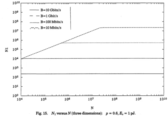
Fig. 15. N versus N (three dimensions): p = 0.6, E0= 1 pJ.
10 May 1994 / Vol. 33, No. 14 / APPLIED OPTICS 2983 B=10 Gbits/s . B=1 Gbit/s B=10Mbits/s __ ________________ ___ ___________ _ ---I . I I . I . I . I.- I . . . I I- ,
n4
&
1V1ll
1010 -4 C12 109 108 107 106 . 10 105 106 107 108 109 1010 NFig. 16. S versusN (three dimensions): B = 100 Mbits/s,p = 0.6, E = 1 pJ. Repeaters are assumed for the all-electrical case.
previous paragraph),
T = max[(N/N1)12d/c, Td]. (29)
Total power 9 is again given by relation (23). The value of N, minimizing .9, , and -simultaneously is
then easily shown to be given by Eq. (25). With this value of N, we find the system linear extent, total power, and delay to be given by
2
= N1/2(kB/Q)/12PE'-/
2P(KY)'/p',(30)
1011 C) 2) UI, -4 V) 109 108 107 106 8 104 105 10.9
= Qy2,and 1/S
= X =max(Y/c, Td), respectively.
Notice that 2 X N112 regardless ofp.
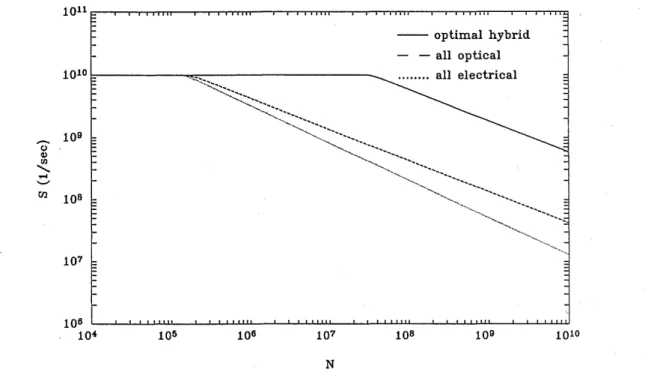
B. Numerical Examples
First considerp = 0.6 and E0 = 1 pJ (Figs. 15 and 16).
Unlike the two-dimensional layout discussed earlier in which the optimal value of S was equal to that for the all-optical case (Fig. 6), here the value of S for the optimal hybrid case is better than that for both all-electrical and all-optical alternatives. With Eqs.
107 108 1010
N
Fig. 17. S versusN(three dimensions): B = 100 Mbits/s,p = 0.8, E = 1 pJ. Repeaters are assumed for the all-electrical case.
2984 APPLIED OPTICS / Vol. 33, No. 14 / 10 May 1994
: I . f a A,, I, ,, I I I,|, I I I a i 1 1 WE . I-!i& r
optimal hybrid - - all optical .all electrical '+s.,9s~~~~~~~~~~~~~~~~~~~~~~~~~~~~~~~~~~~~~~~~~~~~v*;