IMPLEMENTATION OF A CODED-REFERENCE
ULTRA-WIDEBAND SYSTEM
a thesis
submitted to the department of electrical and
electronics engineering
and the graduate school of engineering and sciences
of bilkent university
in partial fulfillment of the requirements
for the degree of
master of science
By
Osman G¨
urlevik
June 2011
I certify that I have read this thesis and that in my opinion it is fully adequate, in scope and in quality, as a thesis for the degree of Master of Science.
Asst. Prof. Dr. Sinan Gezici (Supervisor)
I certify that I have read this thesis and that in my opinion it is fully adequate, in scope and in quality, as a thesis for the degree of Master of Science.
Prof. Dr. Orhan Arıkan
I certify that I have read this thesis and that in my opinion it is fully adequate, in scope and in quality, as a thesis for the degree of Master of Science.
Assoc. Prof. Dr. ˙Ibrahim K¨orpeo˘glu
Approved for the Graduate School of Engineering and Sciences:
Prof. Dr. Levent Onural
ABSTRACT
IMPLEMENTATION OF A CODED-REFERENCE
ULTRA-WIDEBAND SYSTEM
Osman G¨
urlevik
M.S. in Electrical and Electronics Engineering
Supervisor: Asst. Prof. Dr. Sinan Gezici
June 2011
Coded-reference ultra-wideband (CR UWB) systems provide orthogonaliza-tion of the reference and data signals in the code domain to facilitate commu-nications without the need for complex channel estimation and have significant advantages over the previous techniques in terms of performance and/or imple-mentation complexity. This thesis presents a UWB testbed as a general ex-perimental platform to explore pulse-based UWB communications and discusses design and implementation issues. A testbed is built as a flexible solution for hardware implementation of a CR UWB system.
Keywords: Ultra-wideband (UWB), coded-reference (CR), pulse-based UWB
¨
OZET
REFERANS KODLAMALI ULTRA GEN˙IS
¸ BANTLI B˙IR
S˙ISTEM˙IN GERC
¸ EKLENMES˙I
Osman G¨
urlevik
Elektrik ve Elektronik M¨
uhendisligi B¨
ol¨
um¨
u Y¨
uksek Lisans
Tez Y¨
oneticisi: Yrd. Do¸c. Dr. Sinan Gezici
Haziran 2011
Referans kodlamalı ultra geni¸s bantlı sistemler, karma¸sık kanal kestirimine ihtiya¸c duymadan ve ¨onceki tekniklere g¨ore performans veya uygulama a¸cısından ¨
onemli avantajlar elde ederek, ileti¸simi kolayla¸stırmak i¸cin referans ve veri sinyal-lerinin dikgenle¸stirilmesini kod alanında sa˘glar. Bu tezde, darbe tabanlı ultra geni¸s bantlı ileti¸simi incelemek ve tasarım ve uygulama konularını tartı¸smak i¸cin ultra geni¸s bantlı bir sınama ortamı, genel bir deneysel platform olarak sunulmak-tadır. Sınama ortamı, referans kodlamalı ultra geni¸s bantlı bir sistemin donanım uygulaması i¸cin esnek bir ¸c¨oz¨um olarak elde edilmektedir.
Anahtar Kelimeler: Ultra geni¸s bant, referans kodlamalı, darbe tabanlı ultra
ACKNOWLEDGMENTS
I would like to thank my supervisor Asst. Prof. Dr. Sinan Gezici for his time, patience and for guiding my research. Also I would like to thank Prof. Dr. Orhan Arıkan and Assoc. Prof. Dr. ˙Ibrahim K¨orpeo˘glu for their service in my graduate committee. I am grateful to my officemates Dr. Mehmet Burak G¨uldo˘gan, Mehmet Emin Tutay, Ya¸sar Kemal Alp, Aykut Yıldız, Hamza So˘gancı, Ahmet G¨ung¨or and Mert Pilancı.
Contents
1 Introduction 1
1.1 Overview, Objectives and Contributions of the Thesis . . . 1
1.2 Organization of the Thesis . . . 4
2 Signal Model 5 2.1 Transmitted Signal Model . . . 5
2.2 Channel Model and Received Signal Model . . . 6
3 UWB Testbed Design and Implementation 7 3.1 Overview of Transmitter . . . 8
3.2 UWB Transmitter . . . 8
3.2.1 UWB Signal/Pulse Characteristics . . . 8
3.2.2 Transmitter Components and Architecture . . . 11
3.3 Receiver Structures . . . 16
3.4.1 UWB LNA Design . . . 20
3.4.2 Energy Collector . . . 25
3.4.3 Sampling / Analog to Digital Conversion . . . 38
3.4.4 FPGA . . . 41
3.4.5 UWB Antenna . . . 44
3.5 Simulation and Experimental Results . . . 49
3.5.1 Error Probability and Simulation Results . . . 49
3.5.2 Test Environment and Experimental Results . . . 52
4 Conclusions 55
APPENDIX 57
List of Figures
1.1 FCC indoor mask for UWB signals. . . 2
3.1 Time domain waveform of Gaussian derivative pulses. . . 9
3.2 FCC mask and normalized PSD of Gaussian derivative pulses. . . 9 3.3 Time domain waveform of Gaussian derivative pulses. . . 10
3.4 FCC mask and normalized PSD of Gaussian derivative pulses. . . 11
3.5 FCC mask, normalized PSD of Gaussian pulse train generated by TFP1001 Baseband Module and PSD of the received pulse train. . 12
3.6 Typical Gaussian pulses generated by the TFP1001 baseband module. . . 13 3.7 Gaussian pulse train (test-signal) generated by TFP1001 baseband
module. . . 14 3.8 Block diagram of the CR-UWB transmitter. . . 15
3.9 Photo of the constructed CR-UWB transmitter. . . 15
3.10 Block diagram of the CR-UWB receiver which employs symbol rate sampling [1]. . . 16
3.11 Block diagram of the CR-UWB receiver which employs frame rate
sampling [1]. . . 17
3.12 Block diagram of the CR-UWB receiver which employs frame rate sampling. . . 19
3.13 Photo of the constructed CR-UWB receiver which employs frame rate sampling. . . 20
3.14 Biasing circuit of most monolithic microwave amplifiers. . . 22
3.15 Photo of the fabricated Gali-39 PCBA. . . 23
3.16 Recommended placement for the SMT components. . . 24
3.17 Microstripline Line Board . . . 26
3.18 Fabricated Wilkinson power splitter . . . 26
3.19 S-parameter results of the fabricated power splitter board. . . 27
3.20 TB-03 evaluation board. . . 29
3.21 Integrate and dump module. . . 31
3.22 Integrate and dump circuit/Part-1 (recommended placement for the SMT components). . . 32
3.23 Integrate and dump circuit/Part-2 (recommended placement for the SMT components). . . 32
3.24 Integrate and dump circuit scheme. . . 34
3.25 Switching test circuit and switching waveforms, BS270 [2]. . . 35
3.27 Integrator response (simulation output). . . 36
3.28 Integrator response (PCB-scope output). . . 37
3.29 ADC response to test-input signal. . . 38
3.30 TI sampling (reconstruction of an analog signal using an array of four ADCs). . . 40
3.31 FPGA-ADC interface photo. . . 40
3.32 Signal processing diagram implemented on FPGA. . . 42
3.33 Fabricated UWB-circular antenna. . . 45
3.34 VSWR of UWB-circular antenna. . . 46
3.35 R.Loss of UWB-circular antenna. . . 46
3.36 Fabricated UWB-CPW-triangular antenna. . . 47
3.37 Scope-output of received pulse. . . 48
3.38 BEP versus SNR for a single user system with Nf=4, Nf=8, and Nf=16 [3]. . . 51
3.39 A photo of the test environment. . . 52
3.40 BER versus SNR for a single user system for Nf=4 and Nf=8. . . 54
A.1 ((1) and (2): 1x Scaled) - ((3): 2x Scaled) . . . 58
List of Tables
Chapter 1
Introduction
1.1
Overview, Objectives and Contributions of
the Thesis
ULTRA-WIDEBAND (UWB) communications systems are defined as systems that have either an absolute bandwidth of at least 500 MHz or a fractional (relative) bandwidth of larger than %20 [4]. The absolute bandwidth is the difference between the upper frequency, fH, of the −10 dB emission point and
the lower frequency, fL, of the −10 dB emission point [5]; i.e,
B = fH − fL (1.1)
The fractional bandwidth is the ratio of the −10 dB bandwidth occupied by the signal to the center frequency of the signal. The fractional bandwidth is calculated as
Bf rac =
2(fH − fL)
fH + fL
(1.2)
Furthermore, spreading information over a very large bandwidth decreases the power spectral density; hence, a UWB signal can coexist with other systems in the
same frequency range. According to the Federal Communications Commission (FCC) regulations, UWB systems must transmit below certain power levels in order to meet the emissions mask for the appropriate frequency bands [4]. The FCC emission limits for indoor devices are as shown in Figure 1.1.
0 5 10 15 −80 −70 −60 −50 −40 Frequency (GHz)
Power Spectral Density (dBm\Hz)
Figure 1.1: FCC indoor mask for UWB signals.
Since the U.S. FCC approved the limited use of the UWB technology, com-munications systems that employ UWB signals have attracted considerable at-tention. UWB technology is well-suited for a variety of applications such as short-range high-speed data transmission and precise location estimation [6, 7, 8].
UWB communications have traditionally been associated with impulse radio (IR), which is well-suited for low data-rate communications, and most of the academic work on UWB has concentrated on IR [9]. A common technique to implement a UWB-IR communications system is to transmit very short-duration pulses (on the order of 50 ps to 2 ns) with a low duty cycle. In UWB-IR communi-cations systems, a train of pulses is sent per information symbol and information is usually carried by the positions or the polarities of the pulses.
In order to prevent catastrophic collisions among different users and thus provide robustness against multiple access interference, each information symbol
is represented by a sequence of pulses [6]. The symbol duration is divided into Nf
intervals, called f rames, each of which contains one pulse. The pseudo-random sequence that determines the locations of the pulses within the frames is called a time-hopping (TH) code [10]. In a transmitted-reference (TR) system, Nf pulses
are transmitted per information symbol, half of them are used as data pulses, whereas the remaining half are used as reference pulses. Hence, there is no need for channel estimation since the reference and the data pulses are effected by the same channel [11]. However, the main disadvantage of TR UWB receivers is related to the need for an analog delay line to perform data demodulation, which is difficult to build in an integrated manner [12].
In order to realize the advantages of TR UWB systems without the need for an analog delay line, slightly frequency-shifted reference (FSR) UWB systems are proposed [1], [13], where the orthogonality between data and reference pulses is based on a frequency shift rather than a time shift [14], [15]. One limitation of FSR UWB systems is that the orthogonality between the data and reference signals cannot be maintained at the receiver for high data rate systems. Finally, coded-reference (CR) UWB systems are proposed, which provide orthogonaliza-tion of the reference and data signals in the code domain and have significant advantages over the previous techniques in terms of performance and/or imple-mentation complexity [1, 14, 16].
This thesis outlines a UWB testbed as a general experimental platform to explore CR-UWB communications and discusses design and implementation is-sues. The research is motivated by the recently proposed CR-UWB technique to reduce the uncertainty between theoretical expectations and practical implemen-tations. The testbed is built as a flexible solution for hardware implementation of an UWB-IR testbed, and includes a transmitter and a receiver with a sin-gle low-cost UWB planar antenna at each side. To accommodate a number of
features/functions, such as low-complexity reception, programmability and flex-ibility, the testbed is implemented on a field programmable gate array (FPGA) platform and manufactured with high performance plotter for RF and microwave circuitry.
Furthermore, this research presents the design for a pulse-based ultra-wideband communications system capable of supporting data rates of up to 1 Mbps where all baseband and control functions are implemented using FP-GAs. Fundamental items associated with the prototyping, such as manufacture of printed circuit assembly (PCA) and broadband microstrip patch antenna are discussed. System design issues, such as pulse (pattern) generation, synchro-nization, real-time data/signal processing, high-speed analog-to-digital (A/D) conversion are reported detailed in the upcoming chapters also.
1.2
Organization of the Thesis
The remainder of the thesis is organized as follows: In Chapter 2, a signal struc-ture for CR-UWB signals is introduced. The transmitted signal model, channel model and received signal model are presented.
In Chapter 3, UWB transmitter and receiver modules are discussed. Board level design and implementation issues are reported, and then the simulation results and experimental results are presented.
Chapter 2
Signal Model
In this section, first, transmitted signal model for CR-UWB systems is intro-duced. Subsequently, channel model and received signal model are presented.
2.1
Transmitted Signal Model
Consider a pulse based UWB system which transmits the following signal:
s(t) = √ Es 2Nf N∑f−1 j=0 [ajw(t− jTf − cjTc) + b ajw(t− jTf − cjTc− Td) x(t)] , (2.1) where Nf is the number of frames per symbol, Es is the symbol energy, aj ∈
{−1, +1} is the polarity randomization code, w(t) is the UWB pulse with unit
energy, Tf and Tc are frame and chip intervals, cj is the time-hopping (TH) code
and b∈ {−1, +1} is the binary information symbol [1].
In CR-UWB systems, the data and the reference pulses are transmitted at the same time, that is, Td= 0, and x(t) is given by
x(t) =
N∑f−1
j=0
˜
where p(t) = 1 for t ∈ [0, Tf] and p(t) = 0 otherwise, and ˜dj ∈ {−1, +1} is the
jth element of the code that provides data and reference pulses orthogonalization
at the receiver [1, 14].
From (2.1) and (2.2), the transmitted signal in a CR-UWB system is ex-pressed as s(t) = √ Es 2Nf N∑f−1 j=0 aj(1 + b ˜dj) w(t− jTf − cjTc). (2.3)
2.2
Channel Model and Received Signal Model
The following channel model is considered [14]
c(t) =
L
∑
l=1
αlδ(t− τl), (2.4)
where δ(t) is the dirac delta function, αl is the fading coefficient of the lth path
and τl represents the delay of the lth path.
Using the multipath channel model in (2.4) and the transmitted signal in (2.3), the received signal r(t) can be expressed as
˜ r(t) = √ Es 2Nf N∑f−1 j=0 aj(1 + b ˜dj) ˜w(t− jTf − cjTc) (2.5) r(t) = ˜r(t) + n(t) (2.6)
where n(t) is white Gaussian noise and ˜w(t) denoted the convolution of c(t) and w(t); i.e., ˜w(t) = w(t)∗ c(t).
Chapter 3
UWB Testbed Design and
Implementation
This chapter presents an overview of the CR-UWB testbed. First, UWB trans-mitter and receiver modules are discussed. Later, the receiver structures are investigated in this chapter. Board level design and implementation issues, such as pulse (pattern) generation, energy detection and high-speed analog-to-digital (A/D) conversion, are also reported in detail in these parts. Subsequently, the system control part, which is implemented in the receiver-side based on a field programmable gate array (FPGA) platform, and UWB antenna parts are in-troduced. Finally, the Gaussian approximation is employed in order to obtain an approximate closed-form expression for the probability of error. Then, per-formance of various receivers, simulation results, and experimental results are presented.
3.1
Overview of Transmitter
The testbed is built as a flexible solution for hardware implementation of an CR-UWB testbed. For simplicity, burst mode communication is considered in this design. In each burst, a fixed length frame is transmitted, which includes either a pulse or not, without any handshaking between the transmitter and the receiver. Considering high repetition intervals of these short pulses during the operation state, the generation of the information bearing pulses becomes an important issue. To that end, a synthesized function generator is used as an external source to trigger the impulse source.
3.2
UWB Transmitter
3.2.1
UWB Signal/Pulse Characteristics
Various waveforms with complex mathematical formats have been proposed for IR including Gaussian pulse, Gaussian monocycle, and Rayleigh monocycle [17].
The first derivative Gaussian pulses, as given in (3.1), are widely used as the source signal to drive the transmitter in a UWB system.
f (t) = A ( t σ ) e(σt)2 (3.1)
where the pulse parameter A is the maximum amplitude and σ is the pulse half-duration. A small σ corresponds to a narrow waveform in the time domain and a wide bandwidth in the frequency domain.
The normalized source pulses with three different pulse half-duration param-eter (σ) and their power spectral densities (PSD) against the FCC indoor mask are given in Figure 3.1 and Figure 3.2, respectively.
−1 −0.8 −0.6 −0.4 −0.2 0 0.2 0.4 0.6 0.8 1 x 10⁻⁹ −1 −0.8 −0.6 −0.4 −0.2 0 0.2 0.4 0.6 0.8 1 time (s) Amplitude (V) Half−Duration: 600ps Half−Duration: 450ps Half−Duration: 300ps
Figure 3.1: Time domain waveform of Gaussian derivative pulses.
2 4 6 8 10 12 14 −80 −75 −70 −65 −60 −55 −50 −45 −40 Frequency (GHz) PSD (dBm/Hz) Half−Duration : 600ps Half−Duration : 450ps Half−Duration : 300ps FCC Limit
Figure 3.2: FCC mask and normalized PSD of Gaussian derivative pulses.
The peak value position of the PSD and the 10 dB bandwidth increases as
σ decreases. In Figure 3.2 it is observed that when σ = 300ps, the PSD curve
peaks at about 7.5 GHz and 10 dB bandwidth spans from 1.75 GHz to 16 GHz. When σ = 450ps, the PSD curve peaks at about 4.75 GHz and 10 dB bandwidth spans from 1 GHz to 10.5 GHz. Finally when it is increased to σ = 600ps the
PSD curve peaks at about 3.75 GHz and 10 dB bandwidth spans from 0.75 GHz to 8 GHz.
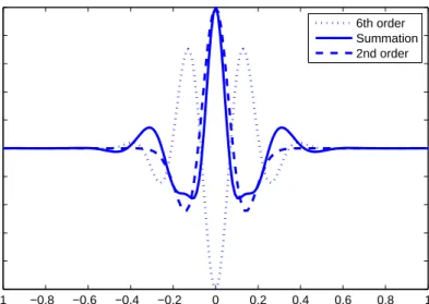
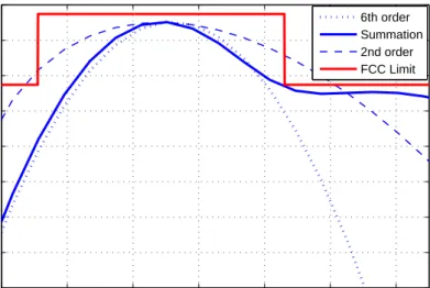
We can generate any higher order derivative Gaussian pulses using lower order pulses. Furthermore, linear combinations of derivative Gaussian pulses may approach the FCC spectral mask better. Figure 3.3 shows the normalized source pulses (a linear combination of a 6th order Gaussian pulse and a 2nd order Gaussian pulse) and Figure 3.4 shows their power spectral densities.
−1 −0.8 −0.6 −0.4 −0.2 0 0.2 0.4 0.6 0.8 1 x 10⁻⁹ −1 −0.8 −0.6 −0.4 −0.2 0 0.2 0.4 0.6 0.8 1 time (s) Amplitude (V) 6th order Summation 2nd order
2 4 6 8 10 12 14 −80 −75 −70 −65 −60 −55 −50 −45 −40 Frequency (GHz) PSD (dBm/Hz) 6th order Summation 2nd order FCC Limit
Figure 3.4: FCC mask and normalized PSD of Gaussian derivative pulses.
Also, it is possible to move the spectra of the first order Gaussian pulse into the UWB band to completely meet FCC’s emission limits, using continuous sine wave carrier [18], [19].
3.2.2
Transmitter Components and Architecture
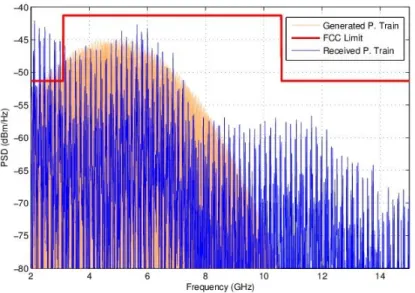
Although the power spectral density of the 2nd order Gaussian pulse cannot fully meet FCC’s emission mask, it is widely used in UWB systems due to its simple waveform which can easily be generated by RF circuits. Furthermore, the pulse generator used in this testbed generates the 2nd order Gaussian-like pulses as well. The measured baseband pulse power spectral density and the received pulse train PSD are shown in Figure 3.5.
Figure 3.5: FCC mask, normalized PSD of Gaussian pulse train generated by TFP1001 Baseband Module and PSD of the received pulse train.
MSSI TFP1001
MSSI TFP1001 is a useful tool for the impulse characterization of UWB systems over the full range of FCC Part 15 Subpart F (UWB) compliance limits (e.g., 3.1-10.6 GHz) [20]. The baseband module actually provides separately triggerable, positive and negative impulses having rise times of typically 250ps, and peak amplitudes of nominally 9 Volts (or +32 dBm) into 50 Ω [21]. Assume that VSWR = 1.00, which means the reflected power from the 50 Ω matched output system (antenna) is %0, the transmitted power is about 1.6 W.
Specifications of TFP1001
• Output Voltage (Magnitude): 9.0 Volts into 50 Ω. • Rise Time: 250 ps (typical)
• Fall Time: 250 ps (maximum) • Pulsewidth: 250 ps (RMS) typical
• Maximum PRF: 100 MHz (minimum) −8 −6 −4 −2 0 2 4 6 8 −1 0 1 2 3 4 5 6 7 time (ns) Amplitude (V)
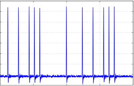
Figure 3.6: Typical Gaussian pulses generated by the TFP1001 baseband module.
As mentioned in the Introduction chapter, UWB systems may cause inter-ferences to other systems since they operate over a large frequency range. The generated UWB pulses are shown in Figure 3.6. The peak to peak voltage (Vpp)
of the pulse is about 7 V, while the duration is approximately 1 ns. In Figure 3.5, the power spectral density (PSD) of the UWB pulse is illustrated. Even though the PSD slightly exceeds the limits in the GPS region (960− 1610 MHz), it is practically compliant with the FCC mask.
Arbitrary Waveform/Pattern Generation
AWC (Arbitrary Waveform Composer) is a menu-based program, which facil-itates the generation and manipulation of arbitrary waveforms on the screen, stores them, and downloads them to the DS345. In order to compose complex arbitrary waveforms, a MATLAB script is written. Generated data file con-tains all information necessary to restore the state of the AWC: waveform data, sampling rate and trigger conditions.
The DS345, in its arbitrary waveform generator mode, has 12-bit vertical resolution and also generates arbitrary waveforms with a fast 40 Msample/s update rate [22]. On the other side, trigger inputs of TFP1001 impulse source respond to the rising edge of the clocking source. Therefore, in order to reach frame intervals of up to Tf = 50 ns, a maximum of 20 MHz square-wave is
generated. To accommodate TFP1001, a minimum of HIGH voltage is adjusted to 3.3 volts because for reliable operation at high pulse repetition frequencies (PRF) up to 100 MHz, it is recommended that the HIGH voltage be at least 3.3 volts and have a pulse width of at least 5 nanoseconds. Generated test waveform, block diagram of transmitter and constructed transmitter are shown in Figure 3.7, 3.8 and Figure 3.9.
−100 −50 0 50 100 −1 0 1 2 3 4 5 6 7 time (ns) Amplitude (V)
Figure 3.7: Gaussian pulse train (test-signal) generated by TFP1001 baseband module.
Figure 3.8: Block diagram of the CR-UWB transmitter.
The impulse outputs are separately triggerable from the BNC connectors on the back panel of the TFP1001 module. For this reason a 50 Ω RG-58/U coaxial cable is used. On the other side, AWC communicates with the DS345 through an RS232 interface. To upload the waveform to the DS345 via the PC, an RS232-DB9 to RS232-DB25 adaptor is used.
3.3
Receiver Structures
The orthogonality between the reference and data pulses is used to estimate the transmitted information symbol b from the received signal in (2.6) [14, 16]. The information symbol is estimated as
ˆ b = sgn {∫ Ts 0 r2(t)x(t)dt } , (3.2)
where sgn{.} is the sign operator and Ts is the symbol interval. The detector in
(3.2) can be implemented as shown in the receiver structure in Figure 3.10.
Figure 3.10: Block diagram of the CR-UWB receiver which employs symbol rate sampling [1].
From (2.2), (3.2) can also be expressed as
ˆb = sgn N∑f−1 j=0 ˜ dj ∫ (j+1)Tf jTf r2(t)dt , (3.3)
where ¯dj ∈ {−1, +1} is the jth element of the code that provides
orthogonal-ization of the data pulses and the reference pulses at the receiver [14]. Further, the expression above suggests another detector implementation based on frame-rate samples [1], as shown in the second structure in Figure 3.11.
Figure 3.11: Block diagram of the CR-UWB receiver which employs frame rate sampling [1].
Let S and ¯S represent the sets of frame indices for which ˜dj = 1 and ˜dj =−1,
and note that both sets include Nf/2 indices for orthogonalization purposes [14];
i.e., | S |=| ¯S |= Nf/2. Then, (3.3) can be expressed as
∑ j∈S ∫ Γj r2(t)dt ˆ b = +1
R
ˆ b =−1 ∑ j∈ ¯S ∫ Γj r2(t)dt . (3.4)which is mainly a non-coherent binary pulse position modulation (PPM) detector [1, 23].
Note that for b = −1, no pulses are transmitted in the frames index by S and the pulses are transmitted in the frames index by ¯S. Similarly, for b = 1, no
pulses are transmitted in the frames index by ¯S and the pulses are transmitted
in the frames index by S [1]. Also comparing the sum of Nf outputs against zero
is equivalent to comparing the sum of the positive outputs against the absolute value of the sum of the negative outputs. The expression in (3.4) can also be
written as [1] H =∑ j∈S ∫ Γj r2(t)dt−∑ j∈ ¯S ∫ Γj r2(t)dt ˆb = +1
R
ˆb =−1 0 . (3.5)Other receiver schemes have been proposed wherein the orthogonality be-tween data and reference pulses is maintained in the time domain and/or in the frequency-domain [13, 14, 15]. In this work, CR UWB systems are investigated and these systems provide orthogonalization of the data and reference signals by separating them in the code domain, which has significant advantages over the previous techniques in terms of performance and/or implementation complexity [1].
The implementation of TR receivers is conditioned by the presence of the delay element. Analog delay lines are difficult to implement with the current technology. For example, in [24] a delay of 20 ns is realized with a 20 foot coaxial cable which is not a viable solution in an integrated receiver [14]. Fur-ther, contrary to FSR systems, for CR UWB systems no frequency conversion is needed. In fact, for the FSR scheme in [14] while the multiplier used before the integrator is an ultra wideband mixer, that in Figure 3.11 is only a sign changer (recall that d =±1).
3.4
Receiver Front-End Implementation
Illustrated in Figure 3.12 and Figure 3.13 are the testbed block diagram and constructed CR-UWB system photo, respectively. Briefly, the incoming pulse to the antenna is strengthened by a UWB low-noise amplifier (LNA) to change the voltage levels and the source current. After that, the received signal is split into two branches and reaches to the squarer followed by the bandpass filter. The
Figure 3.12: Block diagram of the CR-UWB receiver which employs frame rate sampling.
UWB signal is then applied to an energy detector, which comprises an integrator. Finally the digital back ends are implemented in the FPGA unit.
Board level design and implementation are guided by the system design. Some RF circuit simulations are performed first using Proteus ISIS before actu-ally selecting the components. Then, high-speed PCB design and assembly are performed using Proteus ARES, considering signal integrity and electromagnetic interference.
Figure 3.13: Photo of the constructed CR-UWB receiver which employs frame rate sampling.
3.4.1
UWB LNA Design
The amount of signal energy captured by the receiver greatly depends on the amplitude of the incoming signal. The amplifier used in the receiver is the Gali-39 monolithic InGaP HBT MMIC amplifier.
Gali-39 is a wideband amplifier offering high frequency range, DC to 7 GHz. A Darlington amplifier is a 2-port device: RF input, and combined RF output and bias input [25]. One of the most important constraints in the design of the LNA is to achieve a sufficiently large gain and a low noise figure so as not to introduce additional noise. This can be achieved by designing the LNA input to provide an impedance of 50 Ω because the fabricated antenna impedance is 50 Ω.
Specifications of Gali-39
• Gain ≈ 17 dB (f = 1 to 6 GHz ) • Output Power: 10.5 dBm (typically)
• Operating Current: 35 mA (recommended) - 55 mA (max) • Input Power: 13 dBm (max)
Biasing of Monolithic Microwave Amplifiers
Gali-39 operates with a constant-current source that is approximated by a voltage source, an RF choke, and a resistor. As shown in Figure 3.14, the biasing resistor is connected to the designated supply voltage and is given by
Rbias =
Vcc− Vd
Id
, (3.6)
where the bias current is delivered from a voltage supply Vcc through the resistor
Rbias and the RF choke (inductor). A minimum of 2 V drop across Rbias is
required for proper operation [25]. The fabricated circuit is designed to operate with a 12 V DC power supply. For this reason, Rbias = 240 Ω is selected to
ensure recommended device operating current to be Id = 35 mA with a device
voltage of Vd= 3.6V .
The purpose of the RF choke is to minimize the RF loss caused by the resistor. The combined reactance of Rbias and RF choke should be greater than 500 Ω to
reduce gain and power loss at the output. The effects of bias resistor on the output, without an RF choke, can be calculated as follows:
Gloss = 20 log [ (2Rbias+ 50) 2Rbias ] dB . (3.7)
Suppose the use of a 240 Ω bias resistor, without the RF choke in series, will result in 1.6437 dB loss of gain and the power at the output. To prevent this loss, the EPCOS-18nH high frequency surface mount (SMT) resistor is used as an RF choke.
The %2 capacitance tolerance 3.3 nF bypass capacitors at the VCC end of
Rbias are used to prevent coupling from other components via the DC supply line
(e.g. bypass noise of supply voltage).
DC blocking capacitors are also added at the input port and at the output port of the amplifier to prevent the DC current flow-back into the signal source. P./100 nF SMT chip capacitors are used as an external DC blocking capacitor chosen for the frequency of operation.
Figure 3.14: Biasing circuit of most monolithic microwave amplifiers.
As the signal-to-noise ratio (SNR) and the minimum detectable signal is dependent on the noise figure (NF), it is an important parameter for the amplifier stage of the receiver. The noise figure and related equations are described as [26]
Fnoise = Sin/Nin Sout/Nout (3.8) = 1 + Nd GNin (Nd = kT B) (3.9)
where Sin and Nin are, respectively, the signal and noise levels at the input,
Sout and Nout are, respectively, the signal and noise levels at the output, Nd
is the device noise that is due to a passive device held at T = 290 K, G is the device gain, B is the system bandwidth, and k is the Boltzman constant,
k = (1.38x10⁻²³joule/Kelvin).
The common application for noise parameters is the LNA design. In this testbed, an LNA, internally matched to 50 Ω, is used at the front end of the antenna to improve the noise figure of the receiver. In a small surface mount package, the Gali-39 solved the problem by offering noise figures as low as Nf =
2.4 dB.
Printed Circuit Board Assembly (PCBA) of the LNA
The high frequency response of the Gali-39 extends through 7 GHz making it an excellent choice for use of wideband, cellular and other applications. Conversely, constructing test boards for evaluation of these devices, is not straightforward as to make them easy to use by receiver and/or transmitter designer.
Figure 3.15: Photo of the fabricated Gali-39 PCBA.
The photo of the fabricated Gali-39 is shown in Figure 3.15. This board is made from RO4003C material with dielectric constant (at 10 GHz) εr = 3.38±
0.05. Based on past experiences, circuit boards thicker than 0.031 inches are not suitable due to excessive inductance in the ground vias; therefore, the circuit is fabricated on a 0.020 inch (0.508 mm) material with standard 17 µm copper cladding.
The board is tuned for operation in the appropriate frequency bands. The recommended placement for the SMT components is provided in Figure 3.16. The inputs and outputs are connected to SMA female connectors which have 50 Ω impedances and offer excellent electrical performance from DC to 18 GHz. A bias voltage of 12 V is recommended.
RF grounding of pins are important to maintain device stability and RF performance. To minimize thermal impedance, the exposed paddle on the SOT-89 package underside is soldered down to a ground plane along with GND. To connect each of the ground pin to ground plane on the backside of the PCB, various ground vias are placed. Figure 3.16 shows multiple vias that are used to further minimize ground path inductance.
Figure 3.16: Recommended placement for the SMT components.
Furthermore, 0.066 mil wide traces are used with RO4003C material to im-prove the noise figure by additional impedance matching. The output of the Gali-39 is already well matched to 50 Ω and no additional matching is needed.
3.4.2
Energy Collector
The constructed CR-UWB receiver performance greatly depends on the signal amplitude and energy detection. The receiver has no need for sophisticated channel estimation and precise synchronization, which significantly reduces its complexity and cost.
Various modulation schemes, such as OOK, PPM and PAM [23], together with energy detection are reasonable options for the CR-UWB receiver. The re-ceived signal energy can be captured easily using an integrator if the data symbol boundary is roughly known and inter-symbol-interference (ISI) is negligible.
Microstrip Power Splitter Design
In practice, to achieve power division in RF and microwave circuits just by using a tee-junction is not possible because matching of the output ports is necessary for the better power transfer from input to output. Indeed, it can be shown that it is theoretically impossible for a lossless 3-port circuit to be matched at all port [27].
The Wilkinson power divider/combiner uses quarter wave transformers to split the input signal to provide two output signals. The length of the transformer parts are equal to one fourth of the wavelength of the electromagnetic wave. The characteristic impedance (Zo) of a microstrip transmission line can be calculated
Figure 3.17: Microstripline Line Board Zo = 87 √ εr+ 1.41 ln ( 5.98h 0.8w + t ) . (3.11)
The λ/4 microstrip line, characteristic impedance Zo = 70.7Ω on substrate
RO4003C material with dielectric constant (at 10 GHz) εr = 3.38 ±0.05 and
thickness is 0.020 inches (0.508 mm), is approximately 12 mm long at 1 GHz.
The fabricated Wilkinson power splitter in Figure 3.18 , consists of two quar-ter wave matching lines with characquar-teristic impedance ≈ 70.7 Ω and a surface mount, miniature size, 100 Ω resistor. The input and output ports are connected to SMA female connectors which have 50 Ω impedances.
Components
• Input Port - Output Ports • Quarter-Wave Transformers
• Thick Film Resistor, Case Style : 0603; • SMA (female) Connectors
Figure 3.19: S-parameter results of the fabricated power splitter board.
The transient solver is used for the analysis. The S-parameter results of the fabricated model are shown in Figure 3.19. The fabricated microstrip 3 dB
power splitter/combiner shows very good performance in terms of bandwidth and losses. The insertion loss at the center frequency is about 3 dB, the return losses result in 15 dB at port 1, and 15 dB at ports 2 and 3, and the isolation between the output ports reaches 20 dB. However, a 3 GHz microstrip quarter wave matching lines could occupy about 15 cm on PCB, while this fabricated design version occupies less than 4 cm. It should be mentioned that the insertion loss and the isolation of the splitter could be improved by using a multi-layer PCB.
Squarer
A surface mount ADE-42MH+ mixer with wideband and small capacitance is used as the square law device. In order to provide the required level of per-formance, these mixers are generally fabricated monolithically. Following the squarer is a bandpass filter which enables the use of the relative frequency, and a baseband amplifier to interface with the integrator and the A/D converter.
ADE-42MH+ is a double balanced mixer (DBM) that is able to handle the symmetrical topology to remove the unwanted RF/LO input signals from the IF by cancelation [29]. In other words, the LO and RF are balanced so that there is no leakage. Since the constructed testbed operates over a large frequency range, ADE-42MH+ is a good choice of the DBM module where pulses are fine, and may even reduce distortion.
The RF front-end of the UWB receiver is fabricated on an RO4003C sub-strate with a relative dielectric constant of (at 10 GHz) εr = 3.38 ±0.05 and the
thickness is 0.020 inches (0.508 mm). First, it is planned to use the same high-frequency substrate for the mixer as for the receiver. After experiencing SMT assembling and thin copper milling problems, the last decision was to construct the unit on TB-03 evaluation board, which is fabricated on an RO4350 substrate
with a relative dielectric constant of εr = 3.5 ±0.05 and a thickness of 0.030
inches (shown in the Figure 3.20).
Figure 3.20: TB-03 evaluation board.
The employed off-the-shelf board specifications are listed as follows:
Specifications
• low conversion loss, 6.9 dB typ.
• good L-R isolation, 33 dB typ. L-I isolation, 28 dB typ. • low profile package
• freq. range, 5 to 4200 MHz
Using double balanced mixer units is simple; if the user pays attention to some circumstances, they provide excellent multiplication performance. In this constructed testbed, the mixer works in conjunction with the fabricated Wilkin-son power divider/combiner. Also, the double balanced mixers are termination impedance sensitive. They must be terminated with the correct resistive load or
source impedance (normally 50 Ω). To that end, 50 Ω female SMA connectors are chosen for the LO/RF and IF connections.
Integrate and Dump Module
To apply the optimal hypothesis testing procedures that are previously mentioned in this chapter, first a finite number, Nf, of observations are obtained. These
observations are usually obtained from continuous-time observations in various ways [30]. In this work, the employed method for passing from continuous-time to discrete-time is known as integrate-and-dump sampling.
Usually, we measure a signal in the presence of additive noise over some finite number of samples. The integrate and dump block integrates the input signal in discrete time, and resets to zero according to a fixed schedule. In this architecture, the sampling rate selection procedure does not require any information on the bandwidth of the noise. Instead, the sampling interval is selected according to the characteristics of the signal set.
Considering high repetition intervals of the short pulses during the opera-tion state, the operaopera-tion speed of the analog circuit elements and high speed PCB assembling become important issues. To reduce the complexity of the ana-log/hardware design, the integrator part of the testbed is disintegrated into many small parts, various prototypes are fabricated, and in-circuit tests are performed one by one. Finally, the small parts are reconstructed back into a single mod-ule. In the following sections and in Figure 3.21, the constructed final circuit is presented.
Figure 3.21: Integrate and dump module.
In the first prototype, it is fabricated on FR-4 Glass Epoxy natural (yellow) copper clad sheet with a dielectric constant of εr = 4.1, thickness of 0.031 inch,
and a loss tangent (tan δ) of 0.021, which is not constant. A large loss tangent means higher dielectric absorption. Substrates with high loss tangent values affect the high frequency signal on a long line. Dielectric absorption increases attenuation at higher frequencies [31].
The second prototype is fabricated on the substrate RO4003C material with dielectric constant (at 10 GHz) εr = 3.38 ±0.05 and a thickness of 0.020 inches
(0.508 mm), which has stable electrical properties versus frequency. The con-ducting trace is considered as a transmission line. Since a high-frequency signal that propagates through a long transmission line on the PCB is severely affected by the loss tangent of the dielectric material, the third and the final prototype is designed to further minimize the ground path inductance with plated through
holes (vias), which bring the ground to the top side of the circuit and to shorten traces between the vias and power lines as shown in Figure 3.22 and Figure 3.23.
Figure 3.22: Integrate and dump circuit/Part-1 (recommended placement for the SMT components).
Figure 3.23: Integrate and dump circuit/Part-2 (recommended placement for the SMT components).
Features:
• Low-inductance components, such as SMT capacitors with low effective
series inductance, are selected.
• The recommended decoupling capacitors are added to Vcc/GN D pairs.
• Short and wide traces between the vias and capacitor pads are used. • The abruptness of the discontinuity is decreased so that the current flow
will not be disrupted and charge will not accumulate [32].
• The vias are staggered to reduce the crosstalk between them. • Parallel run lengths are minimized between single-ended signals.
An intuitive grasp of the integrator action may be obtained from the current through the feedback loop, which charges the capacitor and is stored there as a voltage from the output to ground. This is a voltage input current integrator [33]. The RC integrator used in the circuit is limited because the current charging the capacitor changes as the capacitor charges up. This means that the circuit integrates only for small voltages and it is suitable for applications where pulses are fine. This integrator works all the way up to the maximum output of the opamp. The output voltage of the opamp is expressed as
ic = C dvc dt Vin R1 = C d dt(−Vo) Vo = VC− 1 R1C ∫ t′ 0 Vin(t)dt , (3.12)
where t is the variable of integration and VC is the voltage across the capacitor
at t′ = 0. The time constant τ = R1C of the integrator needs to be designed
in accordance with the integration time t′ considering the pulse repetition rate (PRR) [34].
Figure 3.24: Integrate and dump circuit scheme.
Note that (3.12) is the output response of the integrator circuit assuming that Vin has zero DC component; otherwise, the charge would store up on the
capacitor and eventually saturate the op-amp. A solution is to use a very large resistor (i.e. a shunt resistor) across the capacitor to minimize the variations in the output voltage. At significantly high frequencies, the resistor has negligible effects. Another solution is to replace the resistor R2 and a reset circuit to
minimize the offset error due to the bias current.
The square of the signal coming from the splitter and the mixer is fed to the integrate and dump unit. Since we are building a UWB-IR system and dealing with short pulses, the integrator circuit has to be very fast. To that end, LMH6702 is selected which is a very wide-bandwidth DC coupled monolithic operational amplifier designed specifically for wide dynamic range systems and radar/communication receivers requiring exceptional signal fidelity [35]. The LMH6702 achieves its excellent pulse and distortion performance by using the current feedback topology.
As it is mentioned, unless the capacitor is periodically discharged, the output will drift outside of the operational amplifier’s operating range. Since we are dealing with short energy samples, the operating switch must be capable of supporting fast switching performance. The BS270 N-Channel Enhancement Mode Field Effect Transistor is the voltage controlled small signal switch with short turn-on and turn-off time down to Ton/of f = 10ns.
Figure 3.25: Switching test circuit and switching waveforms, BS270 [2].
Figure 3.26 illustrates the short pulse train generated by the ISIS simulator transmitter module at a pulse repetition rate (PRR) of 10 MHz. The pulse du-ration is measured at 500 ps, which corresponds to about 2 GHz bandwidth. The maximum pulse rate is assumed up to around 20 MHz because the testbed presents a design for a pulse-based UWB communication system capable of sup-porting data rates of up to 2 Mbps. (For practical reasons data rates of 1 Mbps is used in this testbed.) Sending Nf ≥ 10 at maximum pulse rate results with
a total information symbol duration, Ts ≥ 500ns, in other words at the most 2
Figure 3.26: Simulated pulse.
−500 −400 −300 −200 −100 0 100 200 300 400 500 1.15 1.2 1.25 1.3 1.35 1.4 1.45 1.5 1.55 1.6 time (ns) Amplitude (250mV)
Integrator Output (Scope)
Figure 3.28: Integrator response (PCB-scope output).
Figure 3.27 and Figure 3.28 illustrate simulation and scope outputs of the in-tegrator response. The integrate and dump unit integrates every received squared pulse/signal. The voltage across the capacitor increases at every Tf = 100 ns.
After integrating a few pulses, the efficiency of the integrator starts to decrease. The voltage across the capacitor increases in a normal way, but it is no longer able to hold its level. To avoid the loss of the integrated energy, the voltage is sampled and then reset. In brief, the “integrate and dump” operation is performed.
A resistive network, including TS-53 Single-Turn Cermet Sealed Surface Mount Miniature Trimmer, is used to change the voltage levels of the integra-tor output to valid A/D levels. The fabricated circuit which performs the high bandwidth integration is a combination of both the integrator and the cascaded inverting amplifier array using LMH6702 to provide gain. Passing the pulses through this circuit prior to sampling reduces the required bandwidth of the A/D converter and the signal processor unit (FPGA).
3.4.3
Sampling / Analog to Digital Conversion
The main concern of the testbed is to provide a platform capable of capturing all frame energy in order to realize capabilities of CR-UWB systems. The analog input is squared, the integration is performed using the integrate and dump mod-ule, which is activated by a control signal/synchronizer. Then, the integrated analog signal is converted to a digital signal by a suitable analog-to-digital con-verter (ADC). To this end, the ADC121S101, a low-power, single channel CMOS 12-bit ADC with a high-speed serial interface [36] is used.
Prior to sampling, the pulses are passed through the high bandwidth integrate and dump circuit which reduces the required bandwidth of the A/D converter by preserving the analog integration output during the symbol time Ts. Hence,
the output hold buffer that comes to the ADC is slow in speed which simplifies the ADC design.
Figure 3.29 shows the digital sample of an input test signal comprising a pulse sequence in which, for each transmitted bit, several second-order Gaussian pulses are repeated within a data rate of 2 Mbps.
−200 −150 −100 −50 0 50 100 150 200 0.4 0.45 0.5 0.55 0.6 time (ns) Amplitude (V)
A/D Converter Input
Time Interleaved (TI) Sampling
Time interleaving increases the overall sampling speed of a system by operating two or more data converters in parallel. This sounds reasonable and straightfor-ward but actually requires much more effort than just paralleling two ADCs [37]. Multiple ADCs operate in parallel and their clocks are slightly offset from each other. To drive the Quad ADC input clock in a differential mode, in order to optimize the performance of the ADC network and to reach a sample rate up to 8 Msps, the high-frequency clock synthesizer, CS, is used to generate the sampling clock for the Quad A/D converter. The ADC blocks are written in parallel and are read in serial. After a capture, the FPGA writes the digital data to each sin-gle ADC’s own RAM blocks. The FPGA is then able to reconstruct the received signal as if it were sampled by a single ADC. Since the processor block, FPGA, can read those self blocks intelligently, the sampling rate in this architecture is directly proportional to the ADC number. For practical reasons, in this testbed we use 4 ADC blocks to constitute the Quad ADC network. Furthermore, this number can be increased to construct higher order networks. Figure 3.30 and Figure 3.31 show the Quad ADC network architecture schematic and the FPGA interface photo.
Figure 3.30: TI sampling (reconstruction of an analog signal using an array of four ADCs).
3.4.4
FPGA
The core of the CR-UWB testbed receiver is the digital processing hardware. The digital processing unit must be capable of capturing the incoming data from high speed ADCs, processing the information and produce a response within a specified time. In this testbed, the digital baseband of the UWB-IR receiver is implemented on Xilinx Spartan 3E (Nexys2) FPGA.
The FPGA board, used in the testbed, consists of a high-speed USB-2 port, based on a Cypress CY7C68013A USB controller, to interface FPGA to the PC [38]. The Nexys2 board provides eight 6-pin PMOD connectors that include short circuit protection resistors and protection diodes. PMOD connectors are suitable for drivings peripheral boards with signal rates in excess of 100 MHz, which make them good candidates for high speed A/D converter interfacing.
The communication system is designed to operate at a data rate of 1 Mbps. All algorithms and signal processing tasks are described in VHDL codes and implemented in Xilinx Spartan 3E FPGA. The FGPA performs the following regular receiver baseband functions:
• Controller and Interface (Data Transmission) • Synchronization
• Decoding (Decision)
In the first phase, the FPGA is interfaced to the A/D converter, which fea-tures an 6-lead LLP and SOT-23 package interface, implemented in PMOD sock-ets. Since the ADC121S101 operates with a single supply that can range from +2.7V to +5.25V , FPGA board’s 3.3V supply can successively drive ADC.
Digital Clock Managers (DCMs) are also available to synchronize the FPGA clocks to the external ADC clocks and generate the system clocks needed by the real time processing modules implemented in FPGA (Figure 3.32).
Figure 3.32: Signal processing diagram implemented on FPGA.
A high-frequency clock synthesizer DCMclk and Sclk are used to generate,
respectively, the sampling clock for the A/D converter and the real-time pro-cessing module. In this architecture, Sclk= 100 MHz is the digital clock input.
This clock directly controls the conversion and read-out processes. The output samples are clocked out of this pin on falling edges of the Sclk pin. Lastly, CS=
1µs is the Chip Select signal. On the falling edge of CS, a conversion process begins.
In the second phase, based on the digitally converted values of the integrator outputs, synchronization is achieved. The output format of the ADC121S101
is straight binary. The step size of 1 least significant bit (LSB) width for the ADC121S101 is VA/4096, where VA = 3.3 V is the analog positive supply pin of
the FPGA. The transition from an output code of 0000 0000 0000 to a code of 0000 0000 0001 is at 1/2 LSB, or a voltage of VA/8192. Other code transitions
occur at steps of one LSB [36].
A frame synchronization is made according to a predefined distinctive bit se-quences which are used to indicate the start of the data. It consists of some guard time slots, at the beginning and at the end of the frame, a 24 pilot symbols and 1000 binary information symbols. In the case of any synchronization failure, the process is interrupted. If the synchronization is achieved without any problem, the third phase is activated.
As it is introduced previously, the constructed testbed enables real-time deci-sion on the binary information symbol. The time needed to extract the distinctive ADC RAM blocks and to process the information, is obtained by ADC121S101’s
minimum quiet time. This time gap is required by bus relinquish and the start
of the next conversion [36].
The third phase is the Data Process and Decision part. To apply the optimal hypothesis testing procedures previously derived, first a finite number, Nf, of
observations are obtained. Then, the decision is made according to (3.4) which is expressed as ∑ j∈S ∫ Γj r2(t)dt ˆ b = +1
R
ˆ b =−1 ∑ j∈ ¯S ∫ Γj r2(t)dt . (3.13)Collectively, to observe the code stream and related errors, a display screen is driven by the FPGA module named⟨seven seg⟩. To control the FPGA device further a reset button and switch are also assigned.
3.4.5
UWB Antenna
In order to develop an UWB testbed that satisfy the FCC requirements, it is necessary to design an antenna that employs the following features:
• Compact Size • Low Cost
• Easy to Fabricate
• Covering FCC UWB Frequency Range
Recently, printed slot antennas have attracted much attention due to their low profile, light weight, and ease of integration with monolithic microwave integrated circuits (MMIC) [39]. A printed circular disc monopole antenna is selected to be employed in the testbed because of the low cost, simplicity of design, feeding and geometry [40]. The details of the fabricated design and its experimental results are presented and discussed in this section.
The circular disc monopole with a 50 Ω microstrip feed line is fabricated on the RO4003c material with dielectric constant (at 10 GHz) εr = 3.38 ±0.05 and
thickness of 0.060 inches. To improve the bandwidth, we modify the original ground plane’s height and width. Further changes are made on the radius of the circular monopole disc, the gap between the circular patch and the ground plane in order to get proper impedance matching as well as a huge bandwidth.
As shown in Figure 3.33, the circular disc (where the long axis radius and the short axis radius are equal) and the 50 Ω microstrip feed line are printed on the same side of the dielectric substrate. The width of the microstrip feed line is designed to be 3 mm for the impedance of 50 Ω.
The radius of the circular monopole disc is the first parameter to tune for the lowest return loss and the widest bandwidth, while the other parameters are
Figure 3.33: Fabricated UWB-circular antenna.
kept constant. The first resonant frequency decreases with the increase of the diameter of the disc [40].
To produce a compact size design, the minimum size of the ground plane is suitable where the parameter to study is the length of the ground plane. According to [41], the length of the ground plane has only slight effects on the bandwidth. We select the length of 20 mm for a wider bandwidth and compact size. The conducting ground plane only covers the section of the microstrip feed line and it is printed on the other side of the substrate. The gap (g) between the circular patch and the ground plane below is the most crucial parameter for getting a broad bandwidth [42]. The gap (g=0.5mm) is the selected height of the feed gap between the feed point and the ground plane.
By selecting the parameters mentioned previously, the antenna can be tuned to operate within the desired band. The simulation results are obtained by high-performance RF/uW/Analog/RFIC design and verification tool (Ansoft) (Figure 3.34 and Figure 3.35).
Figure 3.34: VSWR of UWB-circular antenna.
Figure 3.35: R.Loss of UWB-circular antenna.
Associated with an antenna, a number of efficiencies can be defined [43]. One of the most important parameter is the voltage standing wave ratio (V SW R) related to the voltage reflection coefficient (Γ) at the input terminals of the
antenna: Γ = Zin− Z0 Zin+ Z0 (3.14) V SW R = 1+ | Γ | 1+ | Γ | (3.15)
where Z0 is the characteristic impedance of the transmission line and Zin is
the antenna imput impedance. From the simulations obtained, the antenna has
V SW R < 2 and S11<−10 dB in the the frequency span of 2 to 5.75 GHz.
Figure 3.36: Fabricated UWB-CPW-triangular antenna.
Such a planar UWB antenna can be realized by using either a microstrip feed line or a coplanar waveguide (CPW) feeds [44]. In this testbed, another design, a CPW fed rectangular slot antenna [39], which has a simpler structure with one layer of dielectric and metal, is also used. Figure 3.36 shows the structure of the CPW antenna which is printed on an inexpensive FR-4 substrate with the dielectric constant of εr = 4.3 and a substrate thickness of h = 1.5 mm.
Since the information is transmitted using short pulses, it is important to study time domain characteristics of the antenna system. The communica-tion systems for UWB pulse transmission must provide as minimum distorcommunica-tion, spreading, and disturbance as possible. The UWB antenna should be able to transmit the UWB pulse without introducing dispersion effects which result in
significant overlaps at the receiver due to the broadening of the pulses. The printed circular disc monopole antenna is also tested. The received pulse output is shown in Figure 3.37. −25 −20 −15 −10 −5 0 5 10 15 20 25 −0.04 −0.02 0 0.02 0.04 0.06 0.08 0.1 time (ns) Amplitude (V)
Figure 3.37: Scope-output of received pulse.
Measurements are carried out using the designed antenna at the transmitting end and the CPW antenna at the receiving end. It is also shown in [40] that for circular patch structures the ringing effect is slightly higher in the side by side case than the face to face case; however, the amplitude is slightly larger. The designed antenna is used to transmit a second derivative Gaussian pulse and the received third order Gaussian like signal is as shown in Figure 3.37.
3.5
Simulation and Experimental Results
3.5.1
Error Probability and Simulation Results
Considering (2.6) and (2.5), (3.5) can be expressed as
H =∑ j∈S ∫ Γj r2(t)dt−∑ j∈ ¯S ∫ Γj r2(t)dt . (3.16)
Assuming that the noise components are independent for energy samples from different frames (which is approximately true in practice since the frame interval is commonly much larger than the inverse of the bandwidth), we can define random variables H1 and H2 as [1]
H1 = ∑ j∈S ∫ Γj r2(t)dt and H2 = ∑ j∈ ¯S ∫ Γj r2(t)dt . (3.17)
Since n(t) is zero mean Gaussian noise with a flat spectral density of σ2 over
the system bandwidth, the energy samples can be shown to be distributed as chi-square random variables [1, 45]. Therefore, (3.16) can be expressed as
H =∑ j∈S χ2M(θj(b))− ∑ j∈ ¯S χ2M(θj(b)), (3.18)
which can also be written as the difference of two chi-square random variables as [3] H = H1− H2 = χ2Nf M 2 ( ∑ j∈S θj(b) ) − χ2 Nf M 2 ∑ j∈ ¯S θj(b) , (3.19) where χ2
M(θ) denotes a non-central chi-square distribution with M degrees of
freedom and a non-centrality parameter of θ. χ2
M(θ) reduces to a central
chi-square distribution with M degrees of freedom for θ = 0. M is the approximate dimensionality of the signal space, which is obtained from the time-bandwidth product [45] and θj(b) is the signal energy, which can be obtained as
θ = 2EsEw¯ Nf with Ew¯ = ∫ Γj ˜ ω2(t)dt. (3.20)
For a given information symbol b ∈ {−1, +1} with equal probability, the probability of error can be expressed as
Pe=
1
2P{H1 ≤ H2 | b = 1} + 1
2P{H1 > H2 | b = −1} . (3.21)
Clearly, for b = 1, the pulses are transmitted in the frames indexed by S and no pulses are transmitted in the frames indexed by ¯S. Similarly, for b =−1, the
pulses are transmitted in the frames indexed by ¯S and no pulses are transmitted
in the frames indexed by S. Thus H1 and H2 are distributed as follows [3]:
H1(b=1)∼ χ 2 Nf M 2 (θNf/2) and H2(b=1) ∼ χ 2 Nf M 2 (0) (3.22) H1(b=−1) ∼ χ 2 Nf M 2 (0) and H2(b=−1) ∼ χ 2 Nf M 2 (θNf/2) (3.23)
In order to obtain the probability of error expression, the Gaussian ap-proximation is employed as in [3]. For a given binary information symbol
b∈ {−1, +1}, H1 and H2 are Gaussian distributed as follows:
H1(b=1)∼ N ( σ2 NfM 2 + θ Nf 2 , σ 4N fM + 2σ2θNf ) H2(b=1)∼ N ( σ2 NfM 2 , σ 4N fM ) (3.24) H1(b=−1)∼ N ( σ2 NfM 2 , σ 4N fM ) H2(b=−1)∼ N ( σ2 NfM 2 + θ Nf 2 , σ 4N fM + 2σ2θNf ) (3.25)
From (3.24) and (3.25), for a given binary information symbol b, H = H1−H2
is also Gaussian distributed as follows:
H(b=1)∼ N (θ Nf 2 , 2σ 4N fM + 2σ2θNf). (3.26) H(b=−1) ∼ N (−θ Nf 2 , 2σ 4N fM + 2σ2θNf). (3.27)
Therefore, from (3.21), the probability of error can be expressed as
Pe≈ Q ( θNf/2 √ 2σ2N f(M σ2+ θ) ) . (3.28)
Furthermore, from (3.20), the expression above can be stated as Pe ≈ Q ( EsEw¯ √ 2σ2(N fM σ2+ 2EsEw¯) ) . (3.29)
In order to investigate the performance of the receivers for different number of frames Nf, bit error probabilities (BEPs) are obtained for various Nf values
(Nf = 4, Nf = 8, Nf = 16). Figure 3.38 illustrates the BEPs of the receiver for
different number of frames Nf. The BEP performance is expressed as a function
of the signal-to-noise ratio (SNR) Es/N0. From the plots in Figure 3.38, it is
observed that the performance of the receiver degrades as Nf increases, which
is expected from (3.29). For each performance, the frame interval and/or the bandwidth are adjusted to provide the desired M which is determined by the multiplication of the signal bandwidth and the integration interval for the frames. Note that, as explained in [3], the Gaussian approximation gets accurate for large values of M Nf/2. 0 2 4 6 8 10 12 14 16 10−3 10−2 10−1 100 SNR(dB)
Bit Error Probability
Nf=4 Nf=8 Nf=16
Figure 3.38: BEP versus SNR for a single user system with Nf=4, Nf=8, and
3.5.2
Test Environment and Experimental Results
The office layout and antenna positions are illustrated in Figure 3.39. Measure-ments are made while the transmit/receive antennas were within line-of-sight (LOS) of each other. Thirteen transmitter positions, 30 cm to 9 m are surveyed. The transmit antenna is located in the corridor, while the receive antenna is located near the balcony. To prevent variations in the pattern of the receiving and transmitting antennas, all the measurements are performed on the same floor. Further, a 45 cm height tripod is fitted with the receive antenna to avoid changes in antenna angle. The CR-UWB system is calibrated prior to each set of measurements.
Figure 3.39: A photo of the test environment.
The data patterns are observed by the Tektronix scope during the experi-ments. The binary information data collected by the FPGA is analyzed on-line using the code written in VHDL. The 1024 µs size block of the pseudo-random (PN) data is transmitted periodically within a data rate of 1 Mbps. Results for the various transmitter grids are presented in this section.
Data transfer and bit error rate (BER) measurements are performed up to 9 m. (9 m is the maximum direct range achievable inside the Bilkent University EE building). The BER measurements indicate error probabilities of less than 2.3% for ranges up to 5.5 m. Some of the obtained results are summarized in Table 3.1.
Table 3.1: Measurement Results
Distance (m ± 10 cm) BER (Nf = 4) SN R (dB) 9 % 38 0 8.5 % 36 2 8 % 33 4 7.5 % 27.5 6 7 % 18 7 6.5 % 9 9 6 % 4.2 10 5.5 % 2.3 11 4.5 % 0.9 12 3.3 % 0.31 13 1.5 % 0.1 14 0.6 % 0.1 15 0.3 % 0.05 17
Both the theoretical and the experimental results are shown in Figure 3.40, which are in quite good agreement. From the figure, the effects of different Nf
values (Nf = 4, Nf = 8) are observed. As the number of Nf increases, the
performance of the receiver degrades which is expected from (3.29). In (3.29), the BER performance is expressed as a function of the SNR.
0 2 4 6 8 10 12 14 16 10−3 10−2 10−1 100 SNR(dB) BER Theory, Nf=8 Theory, Nf=4 Experimental, Nf=8 Experimental, Nf=4
Figure 3.40: BER versus SNR for a single user system for Nf=4 and Nf=8.
In addition, for the measurements bearing larger Nf values, it is conceivable
to imply that the sample sizes are increased at the cost of a larger noise figure uncertainty. In practice, the integration can be performed over intervals that are smaller than the frame interval in order to collect less noise and increase the SNR [1]. Notwithstanding this apparent simplicity, the testbed is built using off-the-shelf components and is designed with an analog-to-digital (A/D) converter which operates at, the very least, one frame interval.
It can also be observed that the performance differences between approxi-mate values and experimental measurements are increasing for decreasing BER, implying that the temporal variations of the transmit antenna’s elevation and azimuth angles at different ranges become quite coarse.
Chapter 4
Conclusions
In this thesis, implementation of a CR UWB system is studied. The performance of the conventional receiver in multipath fading channels is analyzed wherein the Gaussian approximation is employed in order to obtain an approximate closed-form expression for the probability of error. Further, the constructed testbed is presented, which is built as a flexible solution for the hardware implementation of a CR UWB system. Various measurements and simulations are performed and it is shown that the theoretical and the experimental results for different scenarios are in quite good agreement.
To reduce the uncertainty between theoretical expectations and practical im-plementations and to accommodate a number of features/functions such as low-complexity, programmability and flexibility, various fundamental stages associ-ated with the design and prototyping are clarified in this thesis.
Board level design and implementation are guided by the system design. All necessary simulations are performed in the first place, and then high-speed PCB design and assembly (PCBA) performed. Although this thesis presents the final prototype, considering the importance of high speed PCBA and to reduce the complexity of analog/hardware design, the testbed module is disintegrated into