APPLICATIONS OF PLASMON ENHANCED EMISSION AND
ABSORPTION
A THESIS
SUBMITTED TO THE GRADUATE PROGRAM OF MATERIALS SCIENCE AND NANOTECHNOLOGY
AND THE INSTITUTE OF ENGINEERING AND SCIENCES OF BILKENT UNIVERSITY
IN PARTIAL FULLFILMENT OF THE REQUIREMENTS FOR THE DEGREE OF
MASTER OF SCIENCE
By
Sencer Ayas
December, 2009
ii
I certify that I have read this thesis and that in my opinion it is fully adequate, in scope and in quality, as a thesis for the degree of Master of Science.
Prof. Dr. Salim Çıracı (Supervisor)
I certify that I have read this thesis and that in my opinion it is fully adequate, in scope and in quality, as a thesis for the degree of Master of Science.
Assist. Prof. Dr. Aykutlu Dâna (Co-supervisor)
I certify that I have read this thesis and that in my opinion it is fully adequate, in scope and in quality, as a thesis for the degree of Master of Science.
I certify that I have read this thesis and that in my opinion it is fully adequate, in scope and in quality, as a thesis for the degree of Master of Science.
Assist. Prof. Dr. Ali Kemal Okyay
Approved for the Institute of Engineering and Sciences:
Prof. Dr. Mehmet B. Baray
iv
ABSTRACT
APPLICATION OF PLASMON ENHANCED EMISSION AND
ABSORPTION
Sencer Ayas
M. Sc., Department of Materials Science and Nanotechnology Supervisor: Prof. Dr. Salim Çıracı
December, 2009
The term plasmon-polariton is used to describe coupled modes of electromagnetic waves with electronic plasma oscillations in conductors. Surface plasmon resonances have found profound interest over the last few decades in multiple fields ranging from nanophotonics to biological sensing. In this thesis, we study enhancement of absorption and emission of radiation due to the presence of a modified local electromagnetic mode density within the vicinity of metallic surfaces supporting plasmon modes. Various coupling schemes of free-space electromagnetic modes to plasmon modes are investigated theoretically and experimentally. Local mode densities and field enhancements due to plasmon modes in planar structures, gratings and optical antennas have been studied in their relation to the absorption and emission enhancement of dipoles positioned in various orientations and locations with respect to structures displaying plasmonic effects. Particularly, grating coupled plasmon resonances were analysed using Rigorously Coupled Wave Analysis and Finite Difference Time domain methods. Experimental demonstrations of absorption and emission enhancement of dielectric layers containing Rhodamine 6G on various plasmonic structures are given. Confocal Raman microscopy was used in characterization of fabricated structures. It is seen that the experimental measurements are in good agreement with theoretical predictions. Direction dependent luminescence enhancement is observed with dye molecules on grating structures. Potential applications of plasmon enhanced absorption and emission include high sensitivity absorption spectroscopy, performance enhancement in thin film solar cells and luminescent concentrators.
Keywords: Plasmonics, Emission, Absorption,Grating Coupled Surface Plasmon Resonance, Local
ÖZET
PLASMON ARTTIRIMLI IŞINIM VE EMİLİM UYGULAMALARI
Sencer AyasTez Yöneticisi: Prof. Dr. Salim Çıracı
Yüksek Lisans, Malzeme Bilimi ve Nanoteknoloji Bölümü Aralık, 2009
Plazmon polariton terimi iletkenlerdeki plazma elektronik salınımlarıyla çiftlenmiş elektromanyetik dalga modlarını tanımlamak için kullanılmaktadır. Yüzey plazmon rezonansları son yirmi 30 yilda nanofotonikten ve biyolojik algılamaya kadar birçok alanda geniş merak uyandırmıstır. Bu tezde, plazmon modlarını destekleyen metal yüzeylerin sebep oldugu ışınım ve emilim arttıtrımı lokal elektromanyetik mod yoğunluğuna göre incleledik. Serbest uzay elektromanyetik modlarını, plazmon modlarına çiftleyen değişik uyarılma mekanizmalarını teorik ve deneysel olarak inceledik. Dipollerdeki ışınım ve emilim plazmonik yapıların lokal mod yoğunluğu ve alan arttrımına bağlı olarak çeşitli oryantasyondaki ve plazmonik yapıların değişik yerlerindeki dipollerle inceledik. Kırınım ağına çiftlenmiş plazmon rezonansları RCWA ve FDTD metodlarıyla incelenmiştir. Rhodamine 6G boyasının emilim ve ışınım arttırımı plazmonik yapılarda deneysel olarak gösterilmiştir.Ayrıca konfokal raman mikroskobu florasans karakterizasyounda kullanılmıştır. Teorik sonuçşar ve deneysel sonuçlar birbirini destekler niteliktedir. Ayrıca boya moleküllerinin ışınımının plazmonik kırınım ağı yapılarında yöne bağımlılığı gösterilmiştir. Plazmon arttırımlı ışınım ve emilim uygulama alanları olaraksa, çok hassas emilim spektroskopisi, ince film güneş pillerinde performans arttırımı ve ışıyan yoğunlaştırıcılar olarak gösterilebilir.
Anahtar kelimeler: Plazmonik, Işınım, Emilim, Kırınım ağına çiftlenmiş Plazmon rezonansı, lokal
vi
Acknowledgement
First of all, I would like to express my gratitude to my advisors Prof. Salim Çıracı and Prof. Aykutlu Dana for their support in every aspect of this thesis.
I would like to thank to my thesis committee, Prof. Ceyhun Bulutay and Prof. Ali Kemal Okyay. I would also like to thank to Prof. Mehmet Bayındır for his instrumental support.
I thank to my groupmates: Hasan Güner, Kurtuluş Abak, Mustafa Ürel, Okan Öner Ekiz.
I would also thank to Koray Mızrak for his support on FIB and E-Beam processes. I thank to my office mates, Kurtuluş Abak, Mustafa Ürel, Ali Güneş Kaya, Seydi Yavaş and Mutlu Erdoğan. I would also thank to my precious friends Yavuz Nuri Ertaş.
Figure 2.1 Jablonski diagram for photoluminescence. Incident photon excites the molecule to an upper energy level. By internal mechanisms it decays to low energy level. Then the emitter relaxes to its ground state by emitting a photon………4
Figure 2.2 Illustration of Poynting vector around the system and the dipole to calculate radiation emitted to farfield and total radiated power by the emitter. The integration surface of Poynting vector around the emitter is infinitely small... 12
Figure 3.1 Photonic dispersion curve of photons in air and plasmonic dispersion curve of surface plasmons at metal-dielectric interface. Below 3.61 eV dispersion curves do not intersect except the origin and surface plasmons cannot be excited at metal dielectric interface.(For this simulation silver-air interface)……….15
Figure 3.2 Photonic dispersion curve of photons in air, in glass and plasmonic dispersion curve of surface plasmons at metal-dielectric interface. The photonic dispersion curve of photons and dispersion curve of surface plasmons intersect. Excitation of surface plasmons is possible. (For this simulation air and silver-glass interfaces)……….16
Fig. 3.3 Two prism coupling scheme of surface plasmons. Kretshcmann(a) and Otto(b) configuration. In Kretshcmann configuration, total internal reflection(TIR) takes place. The tail of incident light from prism extended to the metallic region. In Otto configuration attenuated total reflection (ATR) takes place. The tail of incident wave tunnels to the metal surface. Surface plasmons are excited if the horizontal component of momentum of incident light matches the surface plasmons momentum………..17
Figure 3.4 Grating coupling scheme; Incident light is diffracted into many orders. If the horizontal components of momentums of diffracted orders are matched with the surface plasmons momentum on metal dielectric interface, then surface plasmons are excited. At many wavelengths, excitation of surface plasmons are possible……..18
Figure 3.5 Dispersion relation of SPPs. Strong dependence of dispersion relation to the dielectric function is illustrated. Surface plasmons can be excited both on metal-air interface(a) and metal-dielectric interface(b). Dispersion relation due to first three orders are highlighted………..18
viii
Figure 3.6 Reflection and Transmission from a multilayer system. For each interface, backward and forward reflected waves are shown. At each interface horizontal and magnetic fields are matched due to continuity equation Matching horizontal components of electric and magnetic field for each layer iteratively results the relation between incident, reflected and transmitted waves……….. 22
Figure 3.6 Simulated reflectivity vs. angle for Kretschmann coupling scheme using transfer matrix method. Silver is used as metallic layer. For incident wavelength of 532nm, surface plasmons are excited at 45 degrees………..23
Figure 3.7 Dispersion relation for Kretschmann SPP Coupling Scheme obtained using transfer matrix method. For each wavelength angle resolved reflectivity is calculated. The discreteness of curve for higher wavelengths is due to the interpolation of simulation result………... 24
Figure 3.8 Simulated reflectivity vs. angle for Otto coupling scheme using transfer matrix method. Silver is used as metallic layer. For incident wavelength of 532nm, surface plasmons are excited at 45 degrees. Reflectivity strongly depends on the separation between air and metal. For this simulation it is 250nm………...24
Figure 3.9 Dispersion relation for Otto SPP Coupling Scheme obtained using transfer matrix method. For each wavelength angle resolved reflectivity is calculated. The separation is 250nm. Silver is used as metallic layer……….. 25
Figure 3.10 Real and Imaginary parts of y component of electric field distribution for an incidence angle of 45 for Kretschmann coupling scheme. Surface plasmons are excited at metal-air interface. White layer indicates the silver layer. Wavelength of incident light is 532nm ……….……..26
Figure 3.11 Real and Imaginary parts of y component of electric field distribution for an incidence angle of 40 for Kretschmann coupling scheme. Incident light is almost reflected from the silver layer. Wavelength of incident light is 532nm .……….…26
Figure 3.12 Real and Imaginary parts of x component of electric field distribution for an incidence angle of 45 for Otto coupling scheme. Surface plasmons are excited at metal-air interface. The thickness of silver layer assumed infinite. The separation is 250nm. Wavelength of incident light is 532nm ……….……….27
Figure 3.13 Real and Imaginary parts of y component of electric field distribution for an incidence angle of 40 for Otto coupling scheme. Incident light is almost reflected from the silver layer. Surface plasmons are still excited on metal surface. That can be explained from wider reflectivity curve[Fig.3.8]. Wavelength of incident light is 532nm……….. 27
Figure 3.14 Periodically modulated metallic grating structure with a period of p, slit width of d and a film thickness h. In the second region dielectric function can be expanded into Fourier Series due to periodicity of dielectric function. In the second region electric and magnetic field components are written in terms of each diffracted order………..28
Figure 3.15 Illustration of dielectric function in the second region when first three components of fourier coefficient of dielectric function are used. Dielectric function is used in the second region. The structure is assumed infinite in the y plane……….. 33
Figure 3.16 Reflectivity vs. wavelength when the first 3 components of fourier coefficients are used. . n1=1, n3=2.28, θ=0,4 and 8 degrees. period =740nm ……..34
Figure 3.17 Reflectivity vs. wavelength when the first 3 components of fourier coefficients are used. . n1=1, n3=silver, θ=0,4 and 8 degrees. Period =740nm ……..34
Figure 4.1 Emitter on a metallic mirror. The local field intensity or mode density around the emitter and far field radiation depend on the position, polarization and the surrounding medium. Emitter is modeled as classical dipole. Field intensity can be destructive or constructive at the dipole position and at the farfield as the distance to surface changes………... 38 Figure 4.2 Calculated wavelength dependent radiative rate enhancement and quantum yield for both polarizations of dipole on sinusoidal gratings using the method described above. At 760nm, due to enhanced mode density, emission enhancement is more significant[See Fig. 4.4]. The distance of dipole to the surface (d) is 50nm, n0=0.2……….. 39 Figure 4.3 Calculated wavelength dependent radiative rate enhancement and quantum yield for both polarizations of dipole on sinusoidal gratings. The effect of plasmonic mode density is still significant at 760nm. d=500nm, n0=0.2……….…..40 Figure 4.4 Numerical dispersion curve of surface plasmons on sinusoidal gratings. Two parts of dispersion curve intersect at 760nm. Plasmonic mode density can be defined as (dω/dkn)-1 for the curve n. At 760nm two curves intersect and total
x
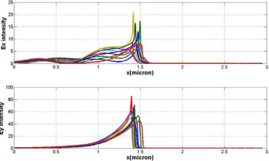
plasmonic mode density is the sum of each curve’s plasmonic mode density. Dispersion curves are calculated using RCWA……….………40 Figure 4.5 Calculated distance dependent radiative rate enhancement and quantum yield for both polarizations of dipole on sinusoidal gratings. Wavelength of the emitter is 400nm. The emission of parallel polarized dipole quenches as the distance decreases [See Fig. 4.7], n0=0.2………..….41 Figure 4.6 Calculated distance dependent radiative rate enhancement and quantum yield for both polarizations of dipole on sinusoidal gratings. Wavelength of the emitter is 800nm. Oscillations are due to decreased wavevector. The emission of parallel dipole quenches as the distance decreases [See Fig. 4.7], n0=0.2……….41 Figure 4.7 Image formation of positive charge, parallel and perpendicular polarized dipoles on a metallic mirror. Images are formed inside the mirror. As the dipole mirror separation decreases, the image of dipole cancels the effect of dipole for parallel polarization, the image of dipole strengthens the effect of dipole for perpendicular polarization ……… 42 Figure 4.8 x and y components of electric field intensity at 760nm.. Perpendicular polarized dipoles are placed on the positions that y component of electric field is enhanced [See Fig. 4.8] ………...43 Figure 4.10 Dipole positions are to examine the effect of electric field distributions(Distribution of plasmonic mode density) for parallel polarization….43 Figure 4.11 Calculated wavelength dependent radiative rate enhancement and quantum yield for perpendicular dipoles on sinusoidal gratings. At the ridges and grooves, the effect of plasmonic mode density at 760 is more significant. At the edges(middle points between grooves and ridges), emission is quenched slightly around 760nm. n0=0.2, d=50nm………..44 Figure 4.12 AFM surface profile and power spectra of biharmonic DVD-R gratings. Two peaks in Power Spectrum indicate the biharmonic surface profile………45 Figure 4.13 Numerical dispersion curve of Surface plasmons dispersion on Biharmonic grating with period 740nm calculated using RCWA. The second harmonic imposed as a second grating with period 370nm. The ratio of amplitudes of harmonics is 0.65. Bandgap formed between 740nm and 810nm……….45 Figure 4.14 x and y components of electric field intensity at 740nm. Perpendicular polarized dipoles are placed on the positions that y component of electric field is enhanced. Parallel polarized dipoles are placed on the positions that x component of electric field is enhanced [See Fig. 4.18]……… 46
Figure 4.15 x and y components of electric field intensity at 810nm. Perpendicular polarized dipoles are placed on the positions that y component of electric field is enhanced. Parallel polarized dipoles are placed on the positions that x component of electric field is enhanced [See Fig. 4.18]………..47 Figure 4.16 Calculated wavelength dependent radiative rate enhancement and quantum yield for parallel dipoles on sinusoidal gratings. Emission is enhanced at edges of bandgap(740nm and 810nm). At the bandgap, emission is quenched significantly. For the positions of dipole[See 4.18]. n0=0.2………..47 Figure 4.17 Calculated wavelength dependent radiative rate enhancement and quantum yield for perpendicular dipoles on sinusoidal gratings. Emission is enhanced or quenched for different positions. Emission enhancement for the positions 1 and 2 at 810nm is due to the enhanced mode density at these points. For positions 3 and 4, emission is quenched at 810nm due to reduced mode density at these points At the bandgap, emission is quenched significantly. For the positions of dipole [See 4.18], n0=0.2………48 Figure 4.18 Dipole positions are to examine the effect of electric field distributions (Distribution of plasmonic mode density) for parallel and perpendicular polarizations……….48 Figure 4.19 Reflectivity vs. angle for sinusoidal gratings, λ=532nm, Period=740nm, metal=silver………...49 Figure 4.20 x and y component of electric field intensity. λ=532nm, θ=20………50
Figure 4.21 Field intensities at different lateral positions on grating. This figure also explains the how much absorption is enhanced for fluorophores that are close to the interface. λ=532nm, θ=20………50 Figure 4.22 Position of fluorophores with respect to tail of SPPs. At the excitation wavelength surface plasmons are excited. Due to enhanced field distribution at excitation wavelength, absorption of fluorophores are enhanced………51
Figure 4.23 Proposed nanoantenna structure. ITO layer is used to prevent charging effect of e-beam lithography. Depending on the gap between silver wires resonance condition of nanoantenna changes……….52
Figure 4.24 Simulated scattering cross section(SCS) of nanoantenna with different gap size………53
Figure 4.25 Electric field intensities for 15nm and 20nm gap sizes………53
xii
Figure 4.27 Simulated radiative rate enhancement and quantum yield for various gap size for parallel polarization. Emission is enhanced around 500nm due to enhanced plasmonic mode density. Around 800nm, quenching of emission is significant due to reduced plasmonic mode density[See SCS calculation Fig. 4.24]. The dipole is at the center of the antenna. no=0.2……….….... 55
Figure 4.28 Simulated radiative rate enhancement and quantum yield for various gap size for perpendicular polarization. Emission is quenched for all wavelengths. Dipole is at the center of antenna. no=0.2………....56
Figure 4.29 Simulated radiative rate enhancement and quantum yield for various vertical position of parallel emitter. Emission enhancement is decreased as dipoles moves vertically due to reduced plasmonic mode density. no=0.2……….56
Figure 4.30 Simulated radiative rate enhancement and quantum yield for various vertical position of perpendicular emitter. Emission is enhanced as the dipole vertically. no=0.2………..57
Figure 4.31 Simulated radiative rate enhancement and quantum yield for various vertical position of parallel emitter. Emission is quenched as the dipole leaves the gap of the antenna. no=0.2……….. 57
Figure 4.32 Simulated radiative rate enhancement and quantum yield for various vertical position of perpendicular emitter. Emission enhancement is significant as the dipole leaves the gap of antenna. no=0.2………. …58
Figure 5.1 Numerical dispersion curves for plasmons on gratings………60
Figure 5.2 Simulated reflectivity vs. angle for 60nm and 120nm groove depths…... 61
Figure 5.3 Simulated Reflectivity vs. groove depth. 65nm groove depth is found optimal for maximum coupling of surface plasmons………..61
Figure 5.4 Simulated Reflectivity for different metal thicknesses. Quality factor of the resonance strongly depend on metal thickness………..62
Figure 5.5 Simulated Absorption for different metal thickness. For infinite thickness metallic film, absorption is maximum………..63
Figure 5.6 Simulated Reflectivity vs. metal thickness. After 80nm film thickness can be assumed infinite………63
Figure 5.7 Fabrication steps (a) DVD-R disc is used as master mold. (b) PDMS is poured on the master mold and cured at 70 0C for 5h. (c) Cured PDMS is peeled off from the master mold and used as elastomeric stamp. (d) Thinned photoresist is spin-coated on SiNx deposited substrate. (e) Elastomeric stamp is released gently on the thin polymer film and hard-baked to make polymer hardened. (f) Elastomeric stamp is mechanically removed from the sample g)Grating profile on Thinned Photoresist h)Transferring of grating structures to Sinx using RIE i)Fabricated Grating structures on SiNx………..65 Figure 5.8 AFM Topography and depth profile of fabricated grating…………..…66
Figure 5.9 Experimental SPP dispersion relation………....67
Figure 5.10 Numerical SPP dispersion relation………..67
Figure 5.11 Absorption and emission spectrum of Rhodamine 6G dye. The wavelength of laser is 532 nm due to absorption maxima at 540nm………..…68 Figure 5.12 Experimental setup we have used to measure absorption enhancement..69
Figure 5.13 Measured fluorescence data with respect to angle. The shift of resonance of surface plasmons are due to the PMMA coating[See 5.14]. At resonance angle(25 degrees), emission is enhanced due to coupling of surface plasmons on gratings. Absorption is enhanced due to enhancement excitation wavelength intensity on gratings. Λ=532nm………..69
Figure 5.14 Simulated reflectance and absorption curves for gratings coated with 20nm PMMA. At 25 degrees surface plasmons are coupled to surface…………..70
Figure 5.15 Fluorescence signals for 10 and 25 degrees. Emission is enhanced due to coupling of surface plasmons on gratings. Absorption is enhanced due to enhancement excitation wavelength intensity on gratings. We defined absorption enhancement as the ration of fluorescence signals of at 555nm(emission maximum for Rhodamine 6G). At 25 degrees surface plasmons are coupled to surface and the photonic mode density at the excitation wavelength increases, so that fluorescence signal intensity increases. Λ=532nm……….71
xiv
Figure 5.16 Measured angular distribution of fluorescence of dye layer on sinusoidal grating. The emission pattern is highly directional. Excitation wavelength is 532nm………71
Figure 5.17 Experimental setup for emission measurements………72
Figure 5.18 Fluorescence image of dye doped PMMA coated grating. The position dependency of emission is apparent on different locations [See Fig. 5.23 for fluorescence data]……….….73
Figure 5.19 Measured Fluorescence intensity of neighbouring ridge and groove of grating. Numerical and experimental data are well matched[See Fig. 5.23 for numerical results]………..73
Figure 5.20 Simulated radiative rate enhancement and quantum yield for parallel and perpendicular polarization. For both polarizations emission is enhanced more on grooves of grating……….74
Figure 5.21 Biharmonic gratings with different depths. Period = 600nm………….75
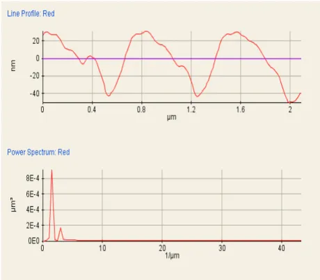
Figure 5.22 Surface profile and topography of fabricated biharmonic gratings. The depth of the grating structures are nearly 45nm………..76
Figure 5.23 Simulated dispersion relation for the biharmonic gratings [See Fig. 5.21]………...76
Figure 5.24 Measured fluorescence signal using micro raman setup. The Excitation wavelength is 532nm. The fluorescence peak at 630nm is due to the enhancement enhanced plasmonic mode density for biharmonic grating [See Fig. 5.23]…………77
Figure 5.25 SEM images of Fabricated nanoantenna structures………78
Figure 5.26 Fluorescence image of dye doped PMMA coated nanoantennas……….79
Figure 5.27 Fluorescence intensity of dye layer on nanoantenna structure[See Fig. 5.25]. Reference signal is the fluorescence of dye layer on glass. Fluorescence signal is enhanced on nanoantenna structure………79
Table of Contents
1 Introduction and Motivation………...1
2Theoretical Background……….3
2.1 Fluorescence……….3
2.2 Absorption Enhancement………..6
2.3 Emission Enhancement……….…9
2.4 Total Emission Enhancement………..13
3 Surface Plasmon Polaritons……….14
3.1 Surface Plasmons……….15
3.2 Excitation of SPPs………...16
3.3 Transfer Matrix Method………..20
3.4 Dispersion of SPPs using TMM………..…24
3.3 Rigorous Coupled Wave Analysis (RCWA) ……….29
4 Simulation of Emission and Absorption Enhancement on plasmonic structures 4.1 Simulation method………...36
4.2 Emission on sinusoidal gratings………..38
4.3 Emission on Biharmonic gratings………...45
4.4 Absorption enhancement on gratings………..50
4.5 Emission on plasmonic nanoantenna strips……….52
5 Experimental Work .………59
5.1 Absorption and Emission Enhancement on Sinusoidal Gratings ……..….59
5.1.1 Optimization, Fabrication and Characterization of Sinusoidal Gratings………..59
xvi
5.2 Emission Enhancement on Biharmonic Gratings………74 5.3 Emission Enhancement on Nanoantenna Strips………..77
6 Conclusion………...80
Chapter 1
Introduction and Motivation
Surface plasmons are charge density oscillations propagating along the metal dielectric interfaces. They are tightly confined to interface and induce an evanescent wave perpendicular to the interface. Due to confinement of plasmonic modes, field intensity enhances enormously at the interface. This unique property of surface plasmons promise several applications in the area of photonics. Metallic surfaces are tailored for exploiting the properties of surface plasmons. Extra Ordinary Transmission (EOT), sub wavelength confinement, low threshold lasers, surface plasmon resonance (SPR) sensors, plasmon enhanced solar cells and plasmon enhanced light emitting devices are realized based on the principles of surface plasmons [1-9].
Fluorescence techniques are widely studied due to their usage in biological imaging, fluorescence sensors and optical microscopy. Pushing the sensitivity up to single photon detection of these devices is now one of the hot topics for scientist and researchers. The absorption and emission properties of emitters strongly depend on not only to the quantum mechanical dynamics, but also the surrounding environment. Modifying the absorption and emission medium changes the fluorescence dynamics. Plasmonic structures are suitable for this aim. In recent studies, fluorescence of molecules are studied on or near plasmonic resonators and antennas both theoretically and experimentally [9-13]. Interaction of optical emitters with surface plasmons in a semiconductor heterostructures and organic polymers are studied with various aspects [14-16].
The motivation behind this thesis was to understand the dynamics of absorption and the emission processes, then integrate this problem with plasmonics. Therefore, in this study, we numerically and experimentally studied both absorption and emission enhancement of fluorophores on or near plasmonic structures. Using the theoretical
2
background, radiative rate enhancement, quantum yield and field distribution calculations were done numerically. Sinusoidal and biharmonic grating structures are fabricated using soft lithography and focused ion beam(FIB) techniques. Nanoantenna strip are fabricated using E-beam lithography technique. We spin coated the fabricated plasmonic structures with Rhodamine 6G doped dye layers and measured the fluorescence signals under different excitation conditions to demonstrate emission and absorption enhancements.
Our contributions can be summarized as follows
1. Simulation of emission properties of optical emitters on different plasmonic structures. Position and polarization dependent emission enhancement of classical dipoles is studied on biharmonic gratings.
2. Process development for the fabrication of sinusoidal gratings using nanoimprint lithography, PDMS moulding, dry etching. Absorption enhancement of Rhodamine 6G is demonstrated due to excitation of surface plasmons.
3. Fabrication of biharmonic gratings using focused ion beam(FIB) techniques and measurement of emission enhancement due to enhancement of plasmonic mode density at the band edges of plasmonic dispersion curves.
The outline of this thesis as follows. In the second chapter, theoretical background of fluorescence, absorption and emission processes is provided by deriving Fermi’s Golden Rule and classical dipole emission. In the third chapter, fundamental properties of surface plasmons and coupling schemes are explained. Transfer matrix method(TMM) and rigorous coupled wave analysis (RCWA) methods are derived. Field distributions, dispersion curves are studied numerically to verify theoretical background. In the fourth chapter, emission and absorption enhancement is simulated for different plasmonic structures. Emission enhancement and quantum yield of emitters are calculated on plasmonic structures. In the fifth chapter, optimization and fabrication of lamellar and sinusoidal gratings are presented. Fluorescence measurements on grating and nanoantenna strips are also provided. In the sixth chapter, we summarize what we have done so far on this subject.
Chapter 2
THEORETICAL BACKGROUND
In this chapter, theoretical background information about fluorescence and photoluminescence is discussed by introducing radiative and non-radiative lifetimes. Absorption enhancement is explained using Fermi’s Golden Rule, which is derived from time-dependent perturbation theory. Then emission of a dipole is described in free space and in the presence of inhomogeneous environment.
2.1 Fluorescence
Fluorophores, molecules and quantum-dot nanoparticles interact with incident photon and absorb it, then re-emit it at a longer wavelength. This process is called fluoroscence. Fluorescence occurs in a certain time period called decay time. Radiative and non-radiative decay are two types of relaxation mechanism in emission process. Non-radiative decay is an internal mechanism of emitter due to the quantum interaction of wave functions of exited states. This mechanism is the lossy mechanism and is the reason for red shift in the emission wavelength and independent of the environment that the emitter is situated. Radiative decay mechanism is directly related to the local electromagnetic density of states. In vacuum, this relaxation process is called spontaneous emission. Due to the dependence on local electromagnetic field of the environment, it can be altered or quenched by changing the photonic mode density of the system. In the emission process, the photonic mode density cannot be changed externally by an excitation mechanism, since once the emitter is excited, decay mechanisms are driven by internally for non-radiative and by its own emission mode density for its radiative decay processes. Therefore, radiative decay rates can only be changed by modifying the mode density at the emission wavelength. Lasers are such devices, working principle based on controlling decay rates and spontaneous emission.
4
In lasers, there occurs coherent population of emitted photon. This process is called stimulated emission.
There are two types of fluorescence processes, Phosphorescence and Photoluminescence. In Phosphorescence, absorbed photons are emitted in much longer time with respect to photoluminescence. The photoluminescence process can be understood from Jablonski diagram [Fig 2.1]. Incident photons excites the molecule to an upper energy level. By internal mechanisms it decays to a lower energy level. Then, the molecule relaxes to its ground state by emitting a photon.
Figure 2.1 Jablonski diagram for photoluminescence. Incident photon excites the
molecule to an upper energy level. By internal mechanisms it decays to low energy level. Then the emitter relaxes to its ground state by emitting a photon
In the emission process, quantum yield or efficiency of an emitter described the ratio of the emitted photons to absorbed photons and given by,
ro o o n (2.1)
where o ronro . o is the total decay rate from an excited state to ground state.
ro
and nro are radiative and nonradiative decay rates. Quantum yield is a measure of the spontaneous emission rate. o and r can be changed by modifying the local photonic mode density. Moreover, Eq.2.1 is defined for vacuum environment and n is o
called intrinsic quantum yield. If the emitter is near a particle, surface or inside a cavity, local photonic mode density changes so that decay rates and quantum yield of the emitter changes. The modified quantum yield is given by,
r
n
(2.2)
where rnrnro. In Eq. 2.2, quantum yield changes due to the change of radiative and total decay rates. The term nr is inserted due to the external losses caused by new environment.
2.2 Absorption Enhancement
Absorption of a photon by a molecule can be understood by means of Time-Dependent Perturbation Theory. It is a well known theory, that explains how the quantum mechanical systems reply to the changes in their environment. One of the main results of Time-Dependent Perturbation Theory is the understanding of light-matter interaction.
To understand the interaction of excitation field with a quantum mechanical system, such as fluorophores, one has to solve Time Dependent Schrodinger’s equation. For the sake of simplicity consider a two level quantum mechanical system with an initial and final states i , f . The wave function of system can be written as,
( ) ( ) f i iE t iE t i i f f a t e a t e (2.3)
Using Eq.2.3 in Schrodinger’s equation we get the coupled equation between a ,i af
given by [18], 1 ( ) if iw t f i f p i da a e H t dt i (2.4) 1 ( ) if iw t i i i p f da a e H t dt i (2.5) withwif (Ef Ei)
6
For starters, to elucidate the interaction of light with an emitter, oscillatory electromagnetic wave nature of light is used. Consider a monochromatic electromagnetic wave that is polarized in the z direction,
( iwt iwt) 2 cos( )
o o
E z E e e z E wt (2.6) This would lead to perturbing Hamiltonian given by,
( ) ( iwt iwt) p o po o H t eE e e z H eE z (2.7)
We assumed this perturbation is on for a certain time interval than it turns off as,
( ) 0 po H t ,t<0 ( ) ( iwt iwt) p po H t H e e z,0<t<to (2.8) ( ) 0 po H t ,t>to
If the system is in the lower energy state i initially, then the probability P of finding system in the final state f is P af 2.
To calculate the probability P, the value of a has to be evaluated after time period f t . o
After some mathematical manipulations, the probability of the system to be found in the final state then becomes [18],
2 2 2 2 2 2 sin(( ) / 2) sin(( ) / 2) ( ) / 2 ( ) / 2 sin(( ) / 2) sin(( ) / 2) 2 cos( ) ( ) / 2 ( ) / 2 if o if o o f i po f if o if o if o if o to if o if o w w t w w t t P a H w w t w w t w w t w w t wt w w t w w t (2.9)
The term with a cosine product in Eq.2.9 is zero. Since, sinc functions decay rapidly after w wif sin(( ) / 2) sin(( ) / 2) 0 ( ) / 2 ( ) / 2 if o if o if o if o w w t w w t w w t w w t (2.10)
We have the transition probability for a two level system, which is initially in the i state as, 2 2 2 2 2 2 sin(( ) / 2) sin(( ) / 2) ( ) / 2 ( ) / 2 if o if o o f i po f if o if o w w t w w t t P a H w w t w w t (2.11)
There are two terms in Eq.2.11. To interpret this formula to the absorption probability, the system has to be in the lower energy state. Then, the first term of Eq.2.11 is zero.
Finally, we have the absorption probability for a two level quantum mechanical system as, 2 2 2 2 2 sin(( ) / 2) ( ) / 2 if o o f i po f if o w w t t P a H w w t (2.12)
If the electromagnetic wave is resonant with this system, absorption process occurs where w w if and we get,
2 2 2 o f i po f t P a H (2.13)
More general form of Eq.2.13 is obtained by inserting the mode density into Eq. 2.12,
2 2 2 2 2 2 2 sin(( ) / 2) ( ) ( ) / 2 2 ( ) if o o f i po f if if if o o f i po f if w w t t P a H g w d w w w t t P a H g w
(2.14)Using Eq. 2.7 in Eq.2.14, we obtain the famous Fermi’s Golden Rule,
2 2 2 ( ) i f if o W
ez g w E (2.15)The main result of this equation turns out that, the absorption rate is directly related the photonic mode density orE , the intensity of incident electric field. 02
8
Finally, the emission enhancement of a emitter due to the intensity enhancement of incident light can be calculated using the formula,
2 . ( ) . ( ) exc o o exc p E I I p E (2.16)
where E is the field intensity in free space, 02 E is the modified field intensity at the 2 emitter position, excis the excitation frequency and p is the polarization of the emitter.
2.3 Emission Enhancement
In the previous chapter, fluorescence enhancement due to the absorption enhancement is derived using time dependent perturbation theory. In this chapter the emission enhancement is going to be explained due to the change in the photonic mode density during the emission process. Rigorous classical oscillator model is used for the derivation of emission. Although classical oscillator model for emission is a quite simple model, it is in good agreement with experimental results. This model gives us two main intuition: Decay rates and frequency shifts. Decay rates are well explained with this model, but in order to calculate frequency shifts due to the changes of mode density, a quantum mechanical approach has to be introduced.
An emitting source can be assumed as a dipole. The emission property of dipoles can be modeled as classical equation of motion which has a dipole moment p, as given below[19,20], 2 2 2 2 o o ( o loc( ))o d p dp e w p p E r dt dt m (2.17) o
is the free space decay rate , w is the oscillation frequency in the absence of o damping , m is the effective mass of the dipole and Eloc( )r is the electric field o induced by dipole at its location.
In free space, right hand side of Eq. 2.17 is zero and written in the form : 2 2 2 o o 0 d p dp w p dt dt (2.18)
while the solution of Eq. 2.18 is 2
o o t iw t o p p e e
If the emitter is in inhomogeneous environment, the solution to Eq. 2.18 is p p eo iwt,
where w is given by [21], 2 2 2 2 2 1 ( ) 2 4 o o o o loc o o o o e w i w p E r w mw p (2.19)
Local electric field is in the same frequency with the oscillatory dipole moment
( ) ( ) iwt loc o loc o E r E r e . Assuming that 2 2 2 ( ) 4 o o loc o o e p E r mp
term is very small compared
to 2
o
w and using the expansion 1 1 2 x x , we get 2 2 2 2 2 (1 ( )) 2 8 2 o o o o loc o o o o e w i w p E r w mw p
(2.20)Eq. 2.20 involves two terms, both decay rate and new oscillation frequency of the dipole. The real part and imaginary part correspond to new oscillation frequency and the new decay rate.
2 2 2 2 2 Re( ( )) 8 2 Im( ( )) o new o o loc o o o o o loc o o o e w w p E r w mw p e p E r mw p (2.21)
Eq.2.21 describes the classical decay rate and oscillation frequency of an classical emitter in inhomogeneous environment. The oscillation frequency of the dipole is red shifted [Eq.2.20]. This result may be misleading but it gives an intuition about shift of emission wavelength of the dipole. On the other hand decay rates go well together
10
with experimental results, full quantum mechanical and semi-classical approaches[13]. If the local electric field is zero in Eq. 2.21, we get free space parameters.
In free space, the radiative decay rate of an optical emitter is given by[22]
2 2 0 3 2 3 ro Ne w mc (2.22)
If we combine Eqs. 2.1-21-22, we get normalized decay rate as follows
3 3 2 3 1 Im( ( )) 2 o o loc o o o o n c p E r w Np
(2.23)where Nis the refractive index. By calculating the induced electric field at the dipole position we can calculate normalized decay rate of any system. However, analytically for most of the systems, it is hard to calculate the electric field distribution. Different solving techniques have been introduced to for mathematically complex system. For instance, dipoles near spherically symmetric particles are solved by using Mie’s Theory[9]. Green Function formalism is used for cylindrically symmetric systems and stratified media[21,23]. Transmittance matrix and plane wave expansion methods are used together to analyze emission on stratified medium[24].
Solving Maxwell’s equations numerically is one of most used techniques for analytically complex systems. Finite Element Method(FEM), Finite Integration Techniques(FIT), Finite Difference Frequency Domain(FDFD) and Finite Different Time Domain Methods are widely used numerical methods[25-28].
Quantum mechanical approach for normalized decay rates is more complex rather than the classical one and is given by [19]
Im{ ( , , )} Im{ ( , , )} p o o o p o p o o o o p n G r r w n n G r r w n (2.24)
where ( , ,G r r wo o o) and G r r wo( , ,o o o) are the Green’s Dyadic Functions in inhomogeneous and free space at ro due to emitter positioned ro. n is the unit vector in p
xx xy xz yx yy yz zx zy zz G G G G G G G G G G (2.25)
One has to calculate ( , ,G r r wo o o) in inhomogeneous environment to calculate normalized decay rate, which is impossible for most of the system. On the other hand field distributions are given by using Green’s Integral equations taken from Ref. [19],
( ) ( , ') ( ') ( ) ( , ') ( ') o o V o o V E r E iw G r r j r H r H iw G r r j r
(2.26)where E and o H are the fields in the absence of source. For a point source or dipole o Eq. 2.26 reduced to by using the relation between current source and dipole moment
( ) o [ o] j r iwp r r 2 ( ) ( , ) ( ) [ ( , )] o o o o o o E r w G r r p H r iw G r r p
(2.27)Using full quantum mechanical approach derived using Dyadic Green Functions along with numerically solving the local electric field distribution, it is possible to obtain normalized decay rates for an emitter. Still we have no information about the radiative and non-radiative decay rates. Radiative decay rate is related to the power radiated to the far field. Dyadic Green Function can be partitioned to near field, intermediate field and far-field terms. Moreover, the relation between the radiative and total decay rates can be written in the form [1,29],
rad r tot P P (2.28)
Where, P is the radiated power to far field and rad P is the total radiated power by the tot dipole. P and rad P can be evaluated by integrating the Poynting vector in the far field tot and around the dipole[Fig. 2.3].
12 Quantum yield or efficiency is the measure of fluorescence in the emission process. It is defined as the ratio of emitted photons to the far field to the absorbed photons. Enhancement of quantum yields leads enhancement of emission process.
Figure 2.2 Illustration of Poynting vector around the system and the dipole to calculate radiation emitted to farfield and total radiated power by the emitter. The integration surface of Poynting vector around the emitter is infinitely small.
2.4 Total Emission Enhancement
Effect of absorption and emission enhancement derived separately. Thus, we have to combine these two terms in order to get a unified relation. As a result total emission enhancement can be written as,
2 2 ( ) ( ) em o o em o p E n w I I n w p E (2.29)
where w is the emission frequency of the emitter. Absorption term can be easily em calculated at the emitter location by normalizing the squared value of electric field to the that of free space. Emission enhancement term is the ratio of the new quantum
efficiency to the intrinsic quantum efficiency. However, for most of the measurement systems we can only collect a small portion of the emitted light to the far field.
Therefore, system collection efficiency has to be accounted. It can be inserted to Eq.2.29 by convolving the far field patterns of the emitters by system’s collection function, which is related to numerical aperture.
14
Chapter 3
SURFACE PLASMON POLARITONS
In this chapter basic information about Surface Plasmon Polaritons (SPPs) is provided. Coupling conditions of light to surface plasmons in different geometries are explained. Field distributions, dispersion diagrams of these geometries are also given. Transfer Matrix formulation for one dimensional multilayer medium is introduced for TE and TM modes. Rigorously Coupled Wave Analysis(RCWA) for one dimensional grating structures is derived..
3.1 Surface Plasmons
Surface plasmons waves are coupled oscillations of photons and electrons at the interface of metals and dielectrics. These waves are tightly confined to the interface, they decay evanescently in the perpendicular direction of the interface. The physics of the SPPs can be understood by deriving dispersion relation of SPPs. The dispersion diagram can be took out by solving Maxwell equations on dielectric-metal interface[30].
Dispersion relation of SPPs at metal dielectric interface can be obtained by solving Maxwell equations for TM polarization. The dispersion relation of surface plasmons is given by, m d x m d w k c (3.1)
Dispersion relation for at silver air interface can be realized as in Fig 3.1 using the measured refractive index data in Ref. 31[31]. The dispersion relation of photons in a dielectric medium is given by,
x d
w k
c
Figure 3.1 Photonic dispersion curve of photons in air and plasmonic dispersion curve of surface plasmons at metal-dielectric interface. Below 3.61 eV dispersion curves do not intersect except the origin and surface plasmons cannot be excited at metal dielectric interface.(For this simulation silver-air interface)
In Fig 3.1, Surface plasmons cannot be directly exited on metal dielectric interface since the dispersion curve of SPPs lies below the dispersion curve of photons. In order to excite surface plasmons at the metal dielectric interface, the slope of photonic dispersion curve has to be changed. This can be done by using techniques such as, prism and grating coupling techniques. Kretschmann and Otto coupling schemes are two prism coupling method to excite surface plasmons.
.
3.2 Excitation of SPPs
The mismatch between the momentums can be altered by using a high refractive index medium. The slope of the photonic dispersion curve decreases, so that plasmonic and photonic can overlap as seen in Fig. 3.2. There are two configuration to excite surface plasmons with prism coupling method. These are Kretschmann and Otto
16
configurations (Fig. 3.3). Otto configuration is a special case of attenuated total internal reflection(ATR). Due to the difficulty of controlling the gap size it is less preferred. In Kretschmann geometry, total internal reflection(TIR) takes place. Tail of the incident light extends to metallic region. If the momentums are matched surface plasmons are excited.
Figure 3.2 Photonic dispersion curve of photons in air, in glass and plasmonic dispersion curve of surface plasmons at metal-dielectric interface. The photonic dispersion curve of photons and dispersion curve of surface plasmons intersect. Excitation of surface plasmons is possible. (For this simulation air and silver-glass interfaces)
Fig. 3.3 Two prism coupling scheme of surface plasmons. Kretshcmann(a) and Otto(b) configuration. In Kretshcmann configuration, total internal reflection(TIR) takes place. The tail of incident light from prism extended to the metallic region. In Otto configuration attenuated total reflection (ATR) takes place. The tail of incident wave tunnels to the metal surface. Surface plasmons are excited if the horizontal component of momentum of incident light matches the surface plasmons momentum.
Another surface plasmon excitation scheme is grating coupling configuration. In gratings the refractive index changes spatially due to the corrugation on the structure. When a light incident on this structure, it diffracts into the many orders that have different momentums. Surface plasmons are excited when the x component of momentum of a diffracted order is equal to surface plasmon momentum vector.
sin( )
spp
k k
mG(3.3)
where G is the grating vector and given by G 2
. is the period of the grating.
The dispersion relation of grating is expressed by inserting Eq.1 into Eq.3 as,
m d spp m d w k mG c (3.4)
18
Figure 3.4 Grating coupling scheme; Incident light is diffracted into many orders. If the horizontal components of momentums of diffracted orders are matched with the surface plasmons momentum on metal dielectric interface, then surface plasmons are excited. At many wavelengths, excitation of surface plasmons are possible.
Surface plasmons are excited at both interfaces of metal. The dispersion relation given by Eq. 3.4 can be plotted at metal air and metal-dielectric interfaces as in Fig. 3.5.. The dispersion curves are calculated for the first three orders. SPPs can be excited by sending light to metal dielectric interface or the metal air interface.
Figure 3.5 Dispersion relation of SPPs. Strong dependence of dispersion relation to the dielectric function is illustrated. Surface plasmons can be excited both on metal-air interface(a) and metal-dielectric interface(b). Dispersion relation due to first three orders are highlighted.
3.3 Transfer Matrix Method
The dispersion relations can be evaluated by using Fresnel formulas derived from the Maxwell Equations. For the structures shown in Fig. 3.3 it can be solved analytically by matching the boundary conditions at the interfaces. On the other hand, Transfer Matrix Method(TMM) which is generally used to calculate transmission and reflection characteristics of a multilayer structure, can be utilized to determine dispersion relation for Kretschmann and Otto SPP coupling schemes. Furthermore, for an arbitrary metallic multilayer structure, dispersion relation can be easily evaluated.
Consider multilayer structure, which has L uniform layers with refractive indices
1, 2, 3... L
n n n n and thicknesses d d d1, 2, 3...d as seen Fig. 3.6. For a TE polarized wave, L Electric fields in each layer can be written in the form,
1z 1z ik xx ik z ik z o E e Re e for z<0 1 ( ) ( ) o l l o l l x k z Z k z Z ik x l l l E A e B e e forZl1 z Zl (3.5) 1z( l) x ik z Z ik x t E Te e for z Z l
where k2zk0 (n22n12sin ( ))2
and l i n( l2n12sin ( ))2 . R and T are the reflection and transmission coefficients. A and B are the amplitudes of electric field in each slab Now we can solve Maxwell equations for each layer. From continuity equations at the boundary of 0th and 1st layers,1 1 1 1 1 1 1 1 0 1 (1 ) [ ] o l o l k d k d z R A B e k i R A B e k at z=0 (3.6)
At the boundary of lth and (l-1)th layer,
1 1 1 1 1 1 1[ 1 1] [ ] o l l o l l o l l o l l k d k d l l l l k d k d l l l l l l A e B A B e A e B A B e (3.7)
20
At the boundary of last layer and (L-1) th layer,
1 0 [ ] o L L o L L k d L L k d z L L L A e B T k A e B i T k (3.8)
From Eqs. 3.6-8 , for an L homogeneous layers there are 2(L equations. These 1) system of equations can be solved simultaneously for R and T by using basic linear algebra techniques for any refractive indices and any number of layers L.
Using Eq. 3.8 at the Lth boundary we get the matrix equation for the A and B coefficients, 1 0 1 1 o L L o L L k d L L z k d L L L A e T k i B e k (3.9)
which can be written in the form of ,
1 1 0 1 1 o L L o L L k d L L z k d L L L A e T k i B e k (3.10)
Coupled equation at the (L-1)th and 1st boundary can also be transformed into matrix form as, 1 1 1 1 1 1 1 1 1 1 o l l o l l o l l o l l k d k d l l k d k d l l l l l l A A e e B B e e (3.11) 1 1 1 1 1 1 1 1 0 0 1 1 1 o l o l k d z z k d A e R k k i i e B k k (3.12)
where Eq. 3.11 is simplified into the equation,
1 1 1 1 1 1 1 1 1 1 1 o l l o l l o l l o l l k d k d l l k d k d l l l l l l A e e A B e e B (3.13)
Let’sdefine, 1 o l l o l l k d l k d l l e V e , 1 1 o l l o l l k d l k d l l e U e , l l l A X B , then Eq. 3.13 can be written as,
1
1 1
l l l l
X U V X
(3.14)
Repeating Eq. 3.14 for each layer, we get the recursive relation between 1st and Lth electric field components,
1 1 1 1 2 L l l L L l X U VU V X
(3.15)By replacing Eqs.3.10-15 into Eq.3.12, we get
1 1 1 1 1 1 1 1 2 0 0 0 1 1 L 1 l l L L z z z l R VU VU V U T k k k i i i k k k
(3.16)which can be simplified as,
1 1 1 1 1 0 0 0 1 1 L 1 l l z z z l R VU T k k k i i i k k k
(3.17) where, 1 o l l o l l k d l k d l l e V e
and 1 1 o l l o l l k d l k d l l e U e
In Eq. 3.17, reflection and transmission coefficients are coupled. To solve this equation, the vector on the right hand side and the vector of the reflection coefficients are combined.
22 Let 1 1 1 0 1 L l l z l W VU k i k
and 1 0 1 z K k i k , then Eq. 3.17 can be written in matrix
form as,
1 0 1 z R K W k i T k (3.18)Finally, reflection and transmission coefficients can be calculated using Eq. 3.18 as,
1 1 0 1 z R K W ik T k (3.19)Figure 3.6 Reflection and Transmission from a multilayer system. For each interface, backward and forward reflected waves are shown. At each interface horizontal and magnetic fields are matched due to continuity equation Matching horizontal components of electric and magnetic field for each layer iteratively results the relation between incident, reflected and transmitted waves.
The formulation for TM-polarization case is quite similar to those of Eqs. 3.5-19,
however lis replaced by l2 l
n
except in the exponents , k and 1z k are replaced by 2z 1 2 1 z k n and 2 2 2 z k n .
3.4 Dispersion of SPPs using TMM
The dispersion curves of SPPs in Otto and Kretschmann configurations can be evaluated by solving directly Maxwell equations at the interface (Fig. 3.1 and 3.2). On the other hand, TMM can be applied to simulate dispersion curves of SPPs for both Otto and Kretschmann configurations. Moreover TMM can also be used to analyze multilayer plasmonic structures, such as MIM(metal insulator metal), IMI(insulator metal insulator). TMM method can also be used to analyze DBR(Distributed Bragg Reflectors). Figure 3.6-7 shows the reflection data for excitation wavelength of 532nm and dispersion curve for Kretschmann configuration. Figure 3.8-9 shows the reflectivity simulation for excitation wavelength of 532nm and dispersion curve for Otto configuration. Refractive index of dielectric layer is 1.5 for both configurations. Silver is used as plasmonic layer with a thickness of 50nm for Kretschmann coupling scheme. For Otto configuration the thickness of silver layer is assumed infinity. All simulations are done for TM polarization, which supports surface plasmon modes.
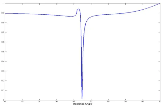
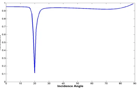
Figure 3.6 Simulated reflectivity vs. angle for Kretschmann coupling scheme using transfer matrix method. Silver is used as metallic layer. For incident wavelength of 532nm, surface plasmons are excited at 45 degrees.
24
Figure 3.7 Dispersion relation for Kretschmann SPP Coupling Scheme obtained using transfer matrix method. For each wavelength angle resolved reflectivity is calculated. The discreteness of curve for higher wavelengths is due to the interpolation of simulation result.
Figure 3.8 Simulated reflectivity vs. angle for Otto coupling scheme using transfer matrix method. Silver is used as metallic layer. For incident wavelength of 532nm, surface plasmons are excited at 45 degrees. Reflectivity strongly depends on the separation between air and metal. For this simulation it is 250nm.
Figure 3.9 Dispersion relation for Otto SPP Coupling Scheme obtained using transfer matrix method. For each wavelength angle resolved reflectivity is calculated. The separation is 250nm. Silver is used as metallic layer.
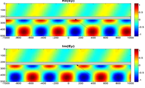
Field distributions of Kretschmann and Otto configurations are shown in Figures 3.10-13. For Kretschmann geometry, an excitation wavelength of 532nm is used. The field distributions at the resonance conditions prove the accuracy of transfer matrix method (TMM). The field distributions are calculated using a commercial FDTD program[28]. From Figures 3.10-11, for Kretschmann configuration y component of electric field intensity increases 30 fold at the metal air interface for an incidence angle of 45 degrees due to reflection minima [Fig. 3.6]
For Otto configuration, Figures 3.12-13 shows us the imaginary and real parts of x component of electric field. The bars on the right hand sides of figures proves the strong coupling of light to surface plasmons to the surface at the reflection minima[Fig. 3.8]
26
Figure 3.10 Real and Imaginary parts of y component of electric field distribution for an incidence angle of 45 for Kretschmann coupling scheme. Surface plasmons are excited at metal-air interface. White layer indicates the silver layer. Wavelength of incident light is 532nm
Figure 3.11 Real and Imaginary parts of y component of electric field distribution for an incidence angle of 40 for Kretschmann coupling scheme. Incident light is almost reflected from the silver layer. Wavelength of incident light is 532nm
Figure 3.12 Real and Imaginary parts of x component of electric field distribution for an incidence angle of 45 for Otto coupling scheme. Surface plasmons are excited at metal-air interface. The thickness of silver layer assumed infinite. The separation is 250nm. Wavelength of incident light is 532nm
Figure 3.13 Real and Imaginary parts of y component of electric field distribution for an incidence angle of 40 for Otto coupling scheme. Incident light is almost reflected from the silver layer. Surface plasmons are still excited on metal surface. That can be explained from wider reflectivity curve[Fig.3.8]. Wavelength of incident light is 532nm