ScienceDirect
Materials Today: Proceedings 18 (2019) 1819–1825 www.materialstoday.com/proceedings
2214-7853 © 2019 Elsevier Ltd. All rights reserved.
Selection and/or Peer-review under responsibility of INTERNATIONAL CONGRESS ON SEMICONDUCTOR MATERIALS AND DEVICES.
ICSMD-2017
Nonlinear Optical Properties of Zinc Oxide Thin Films Produced by
Pulsed Laser Deposition
A. Kepceoğlu
a, S. Yiğit Gezgin
a, Y. Gündoğdu
a, H. Küçükçelebi
a, H. Ş. Kılıç
a,b,*
aSelçuk University, Faculty of Science, Department of Physics, 42000, TURKEY bSelçuk University, High Technology Research and Application Center, 42000, TURKEY
Abstract
In this work, the nonlinear optical properties of Zinc Oxide (ZnO) thin films produced on microscope slide glass substrates at room temperature (RT) using Pulsed Laser Deposition (PLD) method has been presented. PLD system consists of a vacuum chamber (pumped by a turbo molecular pump, backed with a rotary pump), rotating sample and substrate holders, optical thickness measurement system, infrared temperature measurement system and a nanosecond laser system. Previously deposition vacuum chamber evacuated down to ~10-8 mbar and deposition was taken place about 1.3×10⁻¹ mbar oxygen background gas
pressure value. Morphological properties of thin films were obtained by Atomic Force Microscopy (AFM) that shows homogenous and smooth film structure. Thin films crystallinity were investigated by using X-Ray Diffraction (XRD) method and showed that polycrystalline ZnO structure with the largest peak corresponding to (002) orientation but some films contain Zn with (101) orientation . The thicknesses of the films were deduced from reflectance measurement using a fitting software and crosschecked with profilometer and AFM measurements. The thickness of the films ranged between 10 nm and 220 nm. Linear optical properties were obtained by using UV-VIS Spectrometer. Furthermore, we presented the nonlinear optical properties of the ZnO thin films that were obtained by the z-scan method.
© 2019 Elsevier Ltd. All rights reserved.
Selection and/or Peer-review under responsibility of INTERNATIONAL CONGRESS ON SEMICONDUCTOR MATERIALS AND DEVICES.
Keywords: Zinc Oxide Thin Film; Pulsed Laser Deposition; Nonlinear Optical Properties; Z-scan system
* Corresponding author. Tel.: +90-533 365 21 74; fax: +90 332 241 24 99.
1. Introduction
ZnO is a suitable semi-conductor material for optoelectronic applications due to its wide band gap (~3.37 eV), high transparency in visible range of spectrum, low electrical resistance, low toxicity, low cost, high chemical stability, good photo and piezo electric properties. ZnO based materials have been used in many applications related to microelectronics, sensors and optoelectronics[1-3].
ZnO is widely used in solar cell applications as an antireflective coating due to the its low reflectivity and the high transparency in the visible region and opaque behaviour in the UV region[4, 5].
In recent years, the linear and nonlinear optical properties of the ZnO materials have been investigated[6]. Third harmonic generation (THG) parameters were investigated using 1064 nm nanosecond lasers for better understanding the effect of the crystal structure of the thin film on the THG process[7]. Also, different ZnO structures produced with different material doping and using different production methods have been investigated in the literature. Copper doped ZnO was investigated using both ps and ns laser pulses at 532 nm wavelength, and it was revealed that the doping causes some increase in the nonlinear absorption ratio[8]. Similarly, z-scan measurements were obtained by using 532 nm nanosecond laser for aluminium doped ZnO which were produced by sol-gel and PLD methods[9]. Also, gallium [10] or lithium doped[11] ZnO were studied. Self-assembled ZnO thin films exhibit reverse saturable absorption (RSA) effect[12]. The single crystal ZnO thin films having an orientation of (002) shows an active three photon absorption process when femtosecond (fs) laser pulses at 800 nm and the 25 kHz repetition rate[13] were used.
Materials and Methods
Experimental system consists of PLD chamber and laser system. Custom designed (and produced by local industry) vacuum chamber can be evacuated down to ~10-8 mbar and ablation/deposition can be taken at the desired
sample/background pressure values (DUO20M/HiPace700, Pfeiffer Vacuum, Germany). Target and substrate holders are rotated by using two stepper motors and the distance between the target and the substrate was 50 mm. Substrate temperature and the tikness of deposited film can be monitored by using infrared non-contact thermometer (3MH1-CF3, Optris, Turkey) and reflectance measurement system (MProbe In-Situ, Semiconsoft, USA) during the process, respectively. Laser system (Minilite II, Continuum, USA) has 40 mJ laser pulse energy in average at 1064 nm with up to 15 Hz repetition rate. Laser wavelengths from Minilite II laser are available at fundamental, second, third and forth at 1064 nm, 532 nm, 355 nm and 266 nm, respectively. In this work, we use 1064 nm fundamental beam with maximum 40 mJ laser pulse energy and 10 Hz repetition rate to perform PLD. The details of the experimental setup was presented in the literature elsewhere[14, 15]. ZnO sputter target (99.99% purity, Beijing Goodwill Metal, China) at one-inch diameter and 2.5 mm thick was used. Oxygen (O2) gas was used as a reactant.
Microscope slide glass was used as a substrate. Glass slides were washed by soap bubble with hand to remove excess organic dirt after cut, ultrasonificated for 15 minutes in acetone and extra ultasonification was applied for 15 minutes in isopropyl alcohol, nitrogen gas gently blown to glass to evaporate residual alcohol. During the production of the thin films, all parameters (vacuum pressure, target-substrate distance, laser parameters and substrate temperature) was kept constant but only the position of oxygen gas inlet was changed.
Results and Discussion
Before laser ablation process, vacuum chamber was pumped down to a background pressure about a few times 10-8 mbar. As the first preliminary work (Pre1), ZnO material was ablated by laser pulses and sample pressure in
chamber without reactive gas was increased up to 5×10⁻⁶ mbar during the ablation/deposition. In the second
preliminary work (Pre2), oxygen gas was introduced into vacuum chamber as a background gas after chamber evacuated down to 10-8 mbar and chamber pressure was increased upto 5×10⁻³ mbar and experimental work was
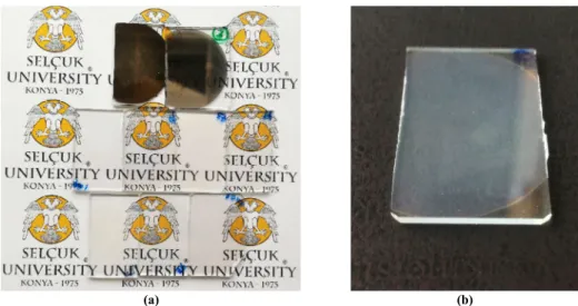
carried out in this reactive gas environment. As seen in Fig. 1(a), these two films (Pre1 and Pre2) were observed to be metallic and given the top of figure 1(a). Pre2 was semi-transparent due to the oxygen gas environment pressure which causes to reduce kinetic energy of the plasma species and reduces film thickness. Seven ZnO thin films
(ZnO1 to ZnO7) were deposited under the (1.30±0.15)×10-1 mbar oxygen gas pressure. All thin films were
transparent as expected and opaque thin film (ZnO) can be seen in Fig. 1(b)
(a) (b) Fig. 1. ZnO thin films were produced by using PLD system, two films in the first line was mostly exhibit Zn
metal film characteristics (Left). Third film (ZnO3) on the black background (Right).
UV-Vis absorption spectra of the ZnO thin films were obtained and presented in Fig.2 (V-670, Jasco Corp., Japan). Absorption spectrum of the ZnO3 films have also presented separately which have intense absorption in the UV region and minimum absorption in the visible region. Band gap value for the ZnO3 thin film was calculated by Tauc plot method by following equation; here (n=1/2, 2, 3/2, 3 allowed direct, allowed indirect, forbidden direct and forbidden indirect transition). Using Tauc plot allowed indirect bandgap value of the ZnO3 thin film was calculated as 3.2 eV which is consistent with the previous works [6, 16-21].
(a) (b) Fig. 2. (a) UV-Vis absorption spectra of the ZnO thin films , (b)Absorption spectrum of the ZnO3 thin film is also presented that shows the
minimum absorption in the visible range where thin film is transparent also Tauc-plot given as an inset.
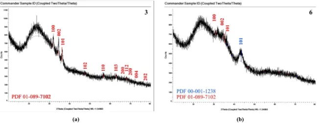
XRD patterns and the analysis of the thin films were obtained by using Bruker AXS/Bruker D8 Advance system. Broad peak around 25˚ comes from the amorphous structure of the glass substrate. XRD peaks revealed that only ZnO3 film produced has no Zn content. Besides, ZnO6 thin film has very broad Zinc diffraction peak which has
(101) orientation (2θ=43.473˚) in fig.3(a). ZnO3 thin film shows in fig.3(b) multi crystalline hexagonal wurtzite phase[22-24] of the lattice structure with three characteristic peaks (100), (002), (101) where 2θ values 30.785˚, 34.291˚ and 35.349˚, respectively, and space group belongs to the P63mc(186). Besides these three peaks, film has more crystalline peaks at the higher angle values. Using Debye-Scherrer formula, we have calculated the average crystallite size of the ZnO sample which is about 17.42 nm and has 0.0068 lattice strain value, which are derived
from the FWHM of the peak (101). We assumed that this multi crystalline structure was formed since we have not heated the substrate.
(a) (b) Fig. 3. XRD spectra of the (a)ZnO3 and (b) ZnO6. Blue lines indicate Zn metallic peak and red lines indicate ZnO peaks.
In Fig. 4, we have presented the AFM images. It can clearly be seen that films have smooth surfaces (in a 25µm×25µm area) and all thin films have surface roughness value lower than the 10 nm. ZnO3 film has particles with the height up to 200nm with columnar structure, and smaller sized particles were also observed.
ZnO1 - 9.2664nm ZnO3 - 7.81423nm ZnO6 - 2.07342nm
(a) (b) (c)
Fig. 4. 2D and 3D AFM images of the (a) ZnO1, (b) ZnO3 and (c) ZnO6 and thin films have low surface roughness values lower than 10 nm.
According to the UV-vis spectra, AFM and XRD results, ZnO3 thin film was chosen to be most suitable one and investigated. In order to present nonlinear properties of ZnO3 thin film, open and closed aperture z-scan measurements were carried out and results are presented in Fig. 5. Z-scan measurements were conducted by changing average laser pulse power from 110 mW to 200 mW. In order to investigate the nonlinear properties of thin film, a fs laser oscillator (Ti:Light, from Quantronix) was used to carry out experimental works. Laser is delivering 90 fs laser pulses with about nJ at 85 MHz repetition rate.
(a) (b) Fig. 5. (a) Open and (b) closed aperture z-scan measurements.
Calculated nonlinear parameters of the ZnO thin film are given in Table.2 and dependencies of the nonlinear absorption coefficient (β) and nonlinear refraction (n2) values on the laser pulse power was measured as a function of
laser power and results are plotted as in Fig. 6. It is clear from plots that absorption coefficient increases while nonlinear refraction index value decreases with increasing laser pulse power. Saturation intensity was calculated to be 2.55×10⁸ W/cm2 by using / formula (here α=1.91×105 cm-1 and β=7.48×10⁻⁴ cm/W) and presented in Fig.6.
Table.2 Measured NLO parameters of the ZnO3 thin film. Β: Nonlinear Absorption Coefficient, n2: third-order nonlinear
refraction coefficient.
Measurement No Laser Power (mW) Intensity I (W/cm2) β (cm/W) n2 (cm2/W)
1 200 2.432·108 6.954·10-4 -2.462·10-6 2 170 3.096·108 7.479·10-4 -1.145·10-6 3 140 3.759·108 3.710·10-4 -0.924·10-6 4 110 4.423·108 2.232·10-4 -0.866·10-6
(a) (b) Fig. 6. Laser pulse power dependant (a) β and (b) n2 values.
Conclusion
As a summary, we have used PLD technique to prepare ZnO thin films on the microscope slide glass substrates at RT. We have shown that the structure of ZnO thin films produced highly depends on the vacuum pressure especially oxygen feeding position to the system. Pure ZnO thin film (ZnO3) was produced when the oxygen gas interacts with the plasma at the laser-target interaction region. UV-Vis results are shown that films are transparent at the visible region and produced thin films can be used as a transparent layer in the photovoltaic devices. Due to the XRD patterns of thin films produced has multi crystalline structure and surface roughness value is lower than the 10 nm. Due to the z-scan measurements, film exhibits saturable absorption and self-defocusing nature under the intense infrared fs laser irradiation.
Acknowledgements
Authors kindly would like to thank,
- Scientific and Technical Research Council of Turkey (TUBITAK) for financial support via Grant No. 1649B031503748,
- Scientific Research Projects Coordination Unit of Selçuk University for financial support via Projects Nos. 14401087, 13301022 and
- Selcuk University, High Technology Research and Application Center for supplying with Infrastructure. The data presented in this work will be as a part of Ph.D. thesis of the Serap YİĞİT GEZGİN.
References
[1] R. Khandelwal et al., "Effects of deposition temperature on the structural and morphological properties of thin ZnO films fabricated by pulsed laser deposition," Optics & Laser Technology, vol. 40, no. 2, pp. 247-251, 2008.
[2] M. Tsoutsouva, C. Panagopoulos, D. Papadimitriou, I. Fasaki, and M. Kompitsas, "ZnO thin films prepared by pulsed laser deposition,"
Materials Science and Engineering: B, vol. 176, no. 6, pp. 480-483, 2011.
[3] Y. Lu et al., "The effect of O 2 partial pressure on the photoluminescence of ZnO thin films grown by pulsed laser deposition," Journal of
Luminescence, vol. 152, pp. 254-257, 2014.
[4] S. K. Singh, P. Hazra, S. Tripathi, and P. Chakrabarti, "Fabrication and experimental characterization of a sol–gel derived nanostructured n-ZnO/p-Si heterojunction diode," Journal of Materials Science: Materials in Electronics, vol. 26, no. 10, pp. 7829-7836, 2015.
[5] R. Pietruszka et al., "Photovoltaic and photoelectrical response of n-ZnO/p-Si heterostructures with ZnO films grown by an atomic layer deposition method," Materials Science in Semiconductor Processing, vol. 25, pp. 190-196, 2014.
[6] A. Zawadzka, P. Płóciennik, Y. El Kouari, H. Bougharraf, and B. Sahraoui, "Linear and nonlinear optical properties of ZnO thin films deposited by pulsed laser deposition," Journal of Luminescence, vol. 169, pp. 483-491, 2016.
[7] A. Zawadzka, P. Płóciennik, J. Strzelecki, and B. Sahraoui, "Transparent amorphous zinc oxide thin films for NLO applications," Optical
Materials, vol. 37, pp. 327-337, 2014.
[8] A. Ryasnyansky et al., "Nonlinear optical absorption of ZnO doped with copper nanoparticles in the picosecond and nanosecond pulse laser field," Applied optics, vol. 44, no. 14, pp. 2839-2845, 2005.
[9] A. Deepthy, D. Ambika, D. G. Sajan, V. Kumar, and V. Nampoori, "Third order nonlinear optical properties of ZnO thin films using z-scan technique," Opt. Commun., vol. 281, 2008.
[10] K. Sandeep, S. Bhat, S. Dharmaprakash, and K. Byrappa, "Influence of Ga doping ratio on the saturable absorption mechanism in Ga doped ZnO thin solid films processed by sol–gel spin coating technique," Journal of Physics D: Applied Physics, vol. 50, no. 9, p. 095105, 2017. [11] T. Anto Johny, V. Kumar, P. Sudheesh, and K. Chandrasekharan, "Nonlinear optical characteristics in lithium substituted ZnO thin films,"
Optics Communications, vol. 309, pp. 279-281, 2013.
[12] L. Irimpan, A. Deepthy, B. Krishnan, L. M. Kukreja, V. P. N. Nampoori, and P. Radhakrishnan, "Effect of self assembly on the nonlinear optical characteristics of ZnO thin films," Optics Communications, vol. 281, no. 10, pp. 2938-2943, 2008.
[13] R. K. Jamal, M. T. Hussein, and A. M. Suhail, "Three-Photon Absorption in Zno Film Using Ultra Short Pulse Laser," Journal of Modern
Physics, vol. 03, no. 08, pp. 856-864, 2012.
[14] S. Y. Gezgin, H. Ş. Kılıç, A. Kepceoğlu, S. Bayır, İ. E. Nalbantoğlu, and A. Toprak, "Plasmonic tuning of gold doped thin films for layers of photovoltaic devices," AIP Conference Proceedings, vol. 1722, p. 200013, 2016.
[15] H. Ş. Kılıç and H. Durmuş, "YENİ BİR PULS LASER DEPOZİSYON (PLD) SİSTEMİ TASARIMI, ÜRETİMİ VE UYGULAMALARI,"
Selçuk Teknik Online Dergi, vol. 15, no. 1, pp. 24-43, 2016.
[16] Z. Qiu et al., "The Influence of Physical Properties of ZnO Films on the Efficiency of Planar ZnO/Perovskite/P3HT Solar Cell," Journal of
[17] J. A. Alvarado, A. Maldonado, H. Juarez, M. Pacio, and R. Perez, "Characterization of nanostructured ZnO thin films deposited through vacuum evaporation," Beilstein J Nanotechnol, vol. 6, pp. 971-5, 2015.
[18] S. A. Vanalakar, G. L. Agawane, A. S. Karnble, C. W. Hong, P. S. Patil, and J. H. Kim, "Fabrication of Cu2SnS3 thin film solar cells using pulsed laser deposition technique," (in English), Solar Energy Materials and Solar Cells, vol. 138, pp. 1-8, Jul 2015.
[19] M. P. Shortell, E. A. Jaatinen, J. Chang, and E. R. Waclawik, "Using pulse transit delay in Z-scan to discriminate between excited-state absorption and other nonlinear processes in ZnO nanocones," Opt Express, vol. 22, no. 6, pp. 6222-8, Mar 24 2014.
[20] P. Singh, A. Kumar, Deepak, and D. Kaur, "Growth and characterization of ZnO nanocrystalline thin films and nanopowder via low-cost ultrasonic spray pyrolysis," Journal of Crystal Growth, vol. 306, no. 2, pp. 303-310, 2007.
[21] S. L. King, J. G. Gardeniers, and I. W. Boyd, "Pulsed-laser deposited ZnO for device applications," Applied surface science, vol. 96, pp. 811-818, 1996.
[22] S. Talam, S. R. Karumuri, and N. Gunnam, "Synthesis, characterization, and spectroscopic properties of ZnO nanoparticles," ISRN
Nanotechnology, vol. 2012, 2012.
[23] M. Bitenc, M. Marinšek, and Z. C. Orel, "Preparation and characterization of zinc hydroxide carbonate and porous zinc oxide particles,"
Journal of the European Ceramic Society, vol. 28, no. 15, pp. 2915-2921, 2008.
[24] J. Zhou, F. Zhao, Y. Wang, Y. Zhang, and L. Yang, "Size-controlled synthesis of ZnO nanoparticles and their photoluminescence properties," Journal of luminescence, vol. 122, pp. 195-197, 2007.