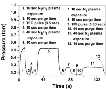
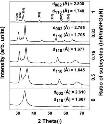
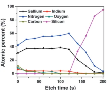
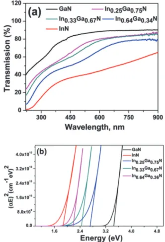
Low-temperature grown wurtzite InxGa1−xN thin films via hollow cathode plasma-assisted atomic layer deposition
Tam metin
Şekil


Benzer Belgeler
distances and angles of the carbazole ring systems (Table 1) are in agreement with each other, as well as with those of related dicarbazoles reported in the literature (Baker et
In particular, we will derive the expressions for the expected cycle length, expected inventory-days (i.e., inventory carried over time) after the lead time period and the
In this study, therefore, we attended to core and peripheral beliefs, examined the influence of language teachers’ contexts on their work and elicited beliefs through the analysis
A total of 120 interior architecture students were sur- veyed about their experiences on five fields of instruction: (1) course design, learning material and electronic
export growth, as was the case in South Korea, Hong Kong, Singapore, and Taiwan ; (2) Turkey has a large population composed of mostly unskilled labor
Since the programmed cell death is a major component of the hepatic regeneration mechanism, and the Bcl-2 family members are the main regulators of this cellular death mechanism,
How- ever, when both the homo and copolymers of PEI with larger molecular weights (PEIs with 25 kDa molecular weight) either linear (L) or branched (B) were used, the plasmid DNA
The corrosion at the source side under a +3 V DC potential was emphasized by comparing the intensity of the Au4f peaks recorded at a particular position d = 0.5 mm corresponding to
