Giant Alloyed Hot Injection Shells Enable
Ultralow Optical Gain Threshold in Colloidal
Quantum Wells
Yemliha Altintas,
†,‡,⊥Kivanc Gungor,
†,⊥Yuan Gao,
§,⊥Mustafa Sak,
†Ulviyya Quliyeva,
†Golam Bappi,
§Evren Mutlugun,
*
,†,‡Edward H. Sargent,
*
,§and Hilmi Volkan Demir
*
,†,∥†Department of Electrical and Electronics Engineering and Department of Physics UNAM− Institute of Materials Science and
Nanotechnology, Bilkent University Ankara 06800, Turkey
‡Department of Materials Science and Nanotechnology and Department of Electrical-Electronics Engineering, Abdullah Gül
University, Kayseri TR-38080, Turkey
§Department of Electrical and Computer Engineering, University of Toronto, 10 King’s College Road, Toronto, ON M5S 3G4,
Canada
∥Luminous! Center of Excellence for Semiconductor Lighting and Displays, School of Electrical and Electronic Engineering, School
of Physical and Mathematical Sciences, School of Materials Science and Nanotechnology, Nanyang Technological University, Singapore 639798, Singapore
*
S Supporting InformationABSTRACT: As an attractive materials system for high-performance optoelectronics, colloidal nanoplatelets (NPLs) benefit from atomic-level precision in thickness, minimizing emission inhomogeneous broadening. Much progress has been made to enhance their photolumines-cence quantum yield (PLQY) and photostability. However, to date, layer-by-layer growth of shells at room temperature has resulted in defects that limit PLQY and thus curtail the performance of NPLs as an optical gain medium. Here, we introduce a hot-injection method growing giant alloyed shells using an approach that reduces core/shell lattice mismatch and suppresses Auger recombination. Near-unity
PLQY is achieved with a narrow full-width-at-half-maximum (20 nm), accompanied by emission tunability (from 610 to 650 nm). The biexciton lifetime exceeds 1 ns, an order of magnitude longer than in conventional colloidal quantum dots (CQDs). Reduced Auger recombination enables record-low amplified spontaneous emission threshold of 2.4 μJ cm−2 under one-photon pumping. This is lower by a factor of 2.5 than the best previously reported value in nanocrystals (6μJ cm−2for CdSe/CdS NPLs). Here, we also report single-mode lasing operation with a 0.55 mJ cm−2threshold under two-photoexcitation, which is also the best among nanocrystals (compared to 0.76 mJ cm−2from CdSe/CdS CQDs in the Fabry−Pérot cavity). These findings indicate that hot-injection growth of thick alloyed shells makes ultrahigh performance NPLs.
KEYWORDS: colloidal quantum wells, nanoplatelets, hot-injection growth, optical gain, single-mode lasing, VCSEL
S
emiconductor nanoplatelets (NPLs), also known as colloidal quantum wells, have attracted great research interest as they allow precise control over their physical thicknesses, which minimizes inhomogeneous broadening and thus enables ultranarrow emission spectra.1,2 Their giant absorption cross-section and oscillator strength,3 stemming from strong carrier confinement in one dimension, make them ideal for colloidal lasers,1,4,5electroluminescent devices,6 solar cells,7and photodetectors.8Compared to the epitaxial growth of inorganic quantum wells, solution-processing of colloidal NPLsoffers low-cost manufacturability and integrability in optoelec-tronics.9
To enable practical colloidal lasers, Auger recombination, which militates against population inversion, needs to be decreased.10 Symmetry breaking in two-dimensional NPLs leads to stricter conservation of momentum and mitigates the
Received: June 25, 2019 Accepted: August 22, 2019 Published: August 22, 2019
Article
www.acsnano.org
effect of the Auger process.11An additional reduction in Auger recombination rates has been shown when a shell is grown on core NPLs.12,13The in-plane delocalization of charge carriers enables the coexistence of multiple excitons and reduces the probability of exciton−exciton annihilation.14A low optical gain threshold and continuous-wave lasing at room temperature have been reported in NPLs.15,16In that respect, shell deposition on NPLs provides a means to further engineer the materials’ optical properties. The compositional adjustment of the shell provides precise control over the effective bandgap of the resulting NPL
heterostructure and thereby the emission peak wavelength. Tuning shell composition also reduces the lattice mismatch associated with the core/shell heterostructure. In addition, shell growth on CdSe core NPLs may improve chemical stability and delete certain trap states by passivating dangling bonds at the surface.
Until now, atomically precise shell formation has commonly been achieved at room temperature using the colloidal atomic layer deposition method (c-ALD).17 The room-temperature shelling process often results in low photoluminescence
Figure 1. (a) Steady-state PL and absorption spectra of CdSe/Cd1−xZnxS core/alloyed g-HIS NPLs. (b) HRTEM images of the samples with different shell compositions. (c) PLQY and PL peak position as a function of the shell composition from 1.00 to 0.50. (d) XRD spectra of the samples. XRD patterns of the zinc-blend (ZB) bulk materials of CdSe (black line), CdS (red line), and ZnS (blue dashed line) were vertically shifted in the graph. (e) XPS spectra of the CdSe/Cd1−xZnxS (x: 0.75) core/alloyed g-HIS NPLs.
quantum yield (PLQY) and poor stability.18−20 Different heterostructures have been realized, such as core/crown,21−25 core/shell,26−29and core/crown/shell.20,30Although PLQY of the NPLs with core/crown structure increases up to 90% in CdSe/CdS,20 and to 95% in CdSe/CdSeTe core/crown NPLs,25 their stability has remained low, curtailing their applications in optoelectronics. Regarding core/shell NPL structures, there are few reports focusing on the enhanced photophysical properties based on the c-ALD approach.14,31Ma et al. have reported a near-unity biexciton QY from NPLs with thin shells using single particle spectroscopy via an optimized c-ALD protocol.14 However, to accurately control the shelling process, the repetitive washing steps are inevitable between successive growths of alternating layers. The Norris group has successfully implemented CdS hot-injection shell growth on CdSe NPLs at 300 °C, yet PLQY of the core/shell NPLs attained a maximum value of 60%.27As has been presented in our previous study, the introduction of the hot injection shell for the synthesis of the NPLs has drastically enhanced by using ZnS HIS the PLQY and stability;32 however, the issue with preserving the high PLQY still remains intact with the introduction of the additional shell layers due to lattice mismatch, a finding ascribed to defect formation.20,30 For a better lattice matched CdSe/CdS core−shell NPLs, the control of Auger recombination rate has been attained by the control of the shell thickness.33 However, due to the small conduction band offset at the CdSe/CdS interface, the electron wave function delocalizes into the CdS shell, and this reduces the optical transition rates and makes emission sensitive to fluctuations in the surrounding dielectric.34
Therefore, there is a strong necessity for an alternative approach providing reduced defect sites and prolonged Auger lifetime in colloidal NPLs.
In this study, we synthesize giant (ca. 4 nm thick) hot injection shelled (g-HIS) NPLs. Such single-step growth of alloyed shells at high temperature enables us to increase the shell thickness and provide strain relaxation. The growth method presented allows not only for the passivation of the surface defects but also the fine-tuning of carrier distribution by engineering the shell composition. As a result of the optimized confinement potential, the biexciton lifetime is prolonged to 1.26 ns, 2.5× the best CdSe/CdS core/shell NPLs,33an order of magnitude longer than conventional nanocrystals,10and three times longer than those with pure ZnS shell, which indicates suppression of nonradiative Auger recombination in these CdSe/CdZnS core/alloyed g-HIS NPLs. Therefore, we observe a record-low optical gain threshold of 2.35μJ cm−2, 2.5× lower than the previously reported best value of chalcogenide semiconductor nanocrystals (6 μJ cm−2).35 Recently, an amplified spontaneous emission (ASE) threshold of 1.2 μJ cm−2has been reported for CsPbBr3nanoparticles; however, their ASE intensity was found to decrease to 70% of its original level after 3.2 × 10⁶ laser pulses.36 Although the halide stoichiometry tunes the emission wavelength of these perovskite nanocrystals,37they suffer from photoinduced phase segregation under photoexcitation.38 Hence, it is challenging to achieve stable laser action with the perovskite nanocrystals at tuned wavelengths. In our proposed alloyed g-HIS growth approach, changing the Cd-to-Zn ratio in the shell enables continuous tuning of the emission wavelength from 610 to 650 nm. After six months of exposure to the ambient environment, these NPLs show excellent stability without appreciable aggregation and maintain at least 95% of their initial PLQY. Furthermore, we did not observe a noticeable decrease in ASE intensity after 2.4× 10⁷
pump pulses. With such high stability, here a single-mode vertical-cavity surface-emitting laser (VCSEL) using these CdSe/CdZnS NPLs as gain medium is demonstrated to lase at a threshold of 0.55 mJ cm−2under two-photon excitation. RESULTS AND DISCUSSION
To improve optical performance and eliminate defects at the core/shell interfaces of NPLs, it is crucial to reduce the 12% lattice mismatch between CdSe and ZnS. In this work, we addressed this problem by introducing alloyed Cd1−xZnxS shells. The fraction of Zn, x, in the shell structure was decreased from 1 to 0.5 by changing the chemical precursor concentration.Figure 1a shows the tunability of photoluminescence (PL) and absorption by changing the shell composition. The PL peak position of the CdSe/ZnS core/HIS NPLs sample is centered at 612 nm with a spectral line width of 24 nm. The PL emission peaks redshifts with increasing Cd-amount in the shell from 612 to 650 nm, and the fwhm of the samples decreases from 24 to 20 nm, as shown in Figure 1a. Uniform growth of the alloyed CdZnS g-HIS on four monolayer (ML) CdSe cores decreased inhomogeneous emission broadening−a finding we attribute to reduced core/shell exciton−phonon coupling.39We imaged the materials using high-resolution transmission electron micros-copy (HRTEM) (Figure S1) and observed uniform coating with shells. The evident red-shifted emission in core/shell NPLs is attributed to electron delocalization into the shell and significantly reduced dielectric confinement.30
High-resolution transmission electron microscopy (HR-TEM) and high-angle annular dark-field scanning transmission electron microscopy (HAADF-STEM) images of the samples with different shell compositions are presented inFigure 1b and
Figure S2. The shape of the core/alloyed shell NPLs changed from an irregular form to almost a square when we increased Cd in the shell (Figure 1b). PLQYs of the samples are shown in
Figure 1c. The best experimental conditions were identified by screening the synthesis parameters such as the concentration of the precursor, ligand, and temperature. For instance, when the injection temperature of the S-precursor was changed from 170 to 190°C, the emission peak wavelength increased from 647 to 664 nm, the fwhm changed from 20 to 25 nm, and PLQY of the sample decreased from 98% to 50%, respectively (Figure S3). The absolute PLQY of CdSe/Cd0.25Zn0.75S core/alloyed g-HIS NPLs is near unity (with an average value 95.8%) at an excitation wavelength of 400 nm (seeTable S1for the data), measured using a calibrated integrating sphere (developed by de Mello et al.) with a precision of ±5%.40 Optical properties of 10 notionally identical CdSe/Cd0.25Zn0.75S core/alloyed g-HIS
NPLs syntheses (Table S1) show reproducibility of the synthesis via the g-HIS growth method. The thickness of the CdSe/Cd0.25Zn0.75S core/alloyed g-HIS NPL was measured 4.7 ± 0.4 nm as obtained from TEM images (Figure S4).
The c-ALD method was previously reported to produce low PLQY and stability when thick shells 3−4 nm are grown: recently, for example, Kelestemur et al.20reported that when the NPL thickness was increased from 1 to 3 MLs, PLQYs of the CdSe/CdS core/shell and CdSe/CdS@CdS core/crown@shell NPLs reduced from 20% to 8% and 36% to 18%, respectively. Similarly, Delikanli et al. have reported that PLQY of the 4 ML CdSe/4 ML CdS core/shell NPLs decreased from 15% to 10% after an additional 2 or 4 ML shell growth.30 The decreased PLQY is ascribed to the formation of defect sites at the interface of the NPLs when using the c-ALD shell growth method. While these core/shell NPLs with both thin and thick c-ALD shells
exhibit low PLQY, core/shell NPLs with thick shells synthesized via g-HIS methods achieve near-unity PLQY.
We observed etching in the 4 ML CdSe core NPLs when these were exposed to high temperatures during the shell growth
(HRTEM images of the CdSe/CdZnS core/alloyed g-HIS NPLs,Figure S5). We distinguish the shell and core of the NPLs from their crystal structural difference. The initial increase in Cd fraction to 0.25 leads to square shapes, while further increasing
Figure 2. ASE spectra of CdSe/Cd1−xZnxS core/alloyed g-HIS NPLs under one-photon (a) and two-photon (b) excitation. ASE peak wavelength and pumpfluence threshold values of NPLs with different shell compositions under one-photon (c) and two-photon (d) excitation. Black squares are averaged thresholds of different measurements with standard deviations, and red circles are the best values for each composition. Pump-fluence-dependent ASE spectra of CdSe/Cd0.25Zn0.75S core/alloyed g-HIS NPLs under one-photon (e) and two-photon (f) excitations. The insets present the evolution of the integrated emission intensity as a function of the pumpfluence, showing superlinear behavior over the threshold.
Cd yields lateral extensions of the NPLs, as shown inFigure S6.
Figures S7 and S8 present additional STEM and energy dispersive X-ray (EDX) characterizations of the samples.
As shown inFigure 1d, the X-ray diffraction (XRD) patterns of the CdSe/Cd1−xZnxS core/shell NPLs are characteristic of
zinc-blende (ZB) (111), (220), and (311) planes. Their broad peaks are accounted for by the nanoscale size of the platelets. XRD patterns shifted to the lower two-θ side when we increased the Cd concentration in the shell: from 44.9° to 44.1° for the (220) plane and 53.1° to 52.2° for the (311) plane, as shown in
Figure 1d. These XRD data confirms the alloyed shell structure of the core/shell nanoplatelets, moving the peak position toward CdS as the Zn concentration is reduced in the shell structure.
X-ray photoelectron spectroscopy (XPS) (Figure 1e and
Figure S9) reveals the known binding overlap of S-2p and Se-3p. Wefit the elemental percentage of the core/shell NPLs based on the area under the curves for Cd-3d, Se-3d, Zn-2p, and S-2p (from the areas under S-2p1/2and S-2p3/2). We then estimated
the atomic ratio of Zn to Cd in the core/HIS NPLs based on XPS measurements and EDX analysis. As the x value was varied from 1.00 to 0.50 in the CdSe/Cd1−xZnxS core/shell NPL
structure, the Zn to Cd ratio decreased from 2.66 to 0.50 and from 2.67 to 0.42 on the basis of XPS and EDX analysis,
respectively (Table S2). The atomic percentage of the elements in the structure for all samples is given inFigure S10. As the composition changed from x = 1.00 to 0.50 in the CdSe/ Cd1−xZnxS core/shell NPLs, a gradual change in the structure of the shell from ZnS to CdZnS was verified with the XPS elemental analysis (Figure S10).
Previous studies that relied on room-temperature shell growth4,20led to reduced optical gain thresholds in such shelled NPLs. We evaluated the optical gain performance of g-HIS NPLs under one- (1PA,λex= 400 nm) and two-photon (2PA,λex
= 800 nm) absorption excitation conditions with a pulse duration of 150 fs and a repetition rate of 1 kHz. Spin-deposited films on fused silica were excited using a stripe-shaped beam formed using a cylindrical lens. Waveguide-coupled emission was collected from the edge of the substrate using a fiber-coupled spectrometer. InFigure 2a,b, ASE spectra of NPLs with different shell compositions are shown under 1PA and 2PA excitation. As shown inFigure 2c,d, the ASE peak wavelength can be tailored from 630 to 670 nm by tuning the shell composition of these NPLs.
ASE measurements show that x = 0.75 (CdSe/Cd0.25Zn0.75S
core/alloyed g-HIS) NPLs have an averaged threshold of 5.3μJ cm−2(minimum of 2.35μJ cm−2) for 1PA and 0.87 mJ cm−2
Figure 3. Magnitude of thefirst bleaching band of (a) x = 0.50, (b) x = 0.75, (c) x = 0.90, and (d) x = 1.00 CdSe/Cd1−xZnxS core/alloyed g-HIS NPLs as a function of the pumpfluence (averaged electron−hole pair created in each NPL). The data trace is normalized to match their long-term decay values.
(minimum of 0.52 mJ cm−2) for 2PA photoexcitation, as seen in
Figure 2c,d. To the best of our knowledge, this is the lowest reported 1PA ASE threshold value among all chalcogenide semiconductor nanocrystal systems.4,11,20,41The ASE measure-ment was also carried out under optical pumping by a nanosecond laser (Figure S11). The increased energy offset barrier between core and shell limits the extension of electron and hole wave functions into the shell, and this decreases the impact of the surface traps and increases the overlap of electron and hole wave functions.42,43We show pump- fluence-depend-ent ASE for the x = 0.75 in Figure 2e,f for 1PA and 2PA, respectively. All of the curves show red-shifted ASE with respect to the PL peaks due to multiexciton interaction in type-I nanocrystals.44The insets display the evolution of the integrated emission intensity as a function of the pumpfluence: a clear threshold is seen to separate the superlinear ASE regime from the linear spontaneous emission regime. Gain stability was measured for different shell compositions (Figure S12): at 2x threshold, the CdSe/Cd0.25Zn0.75S core/alloyed g-HIS NPLs exhibited no decrease in ASE intensity over the course of 6 h of optical pumping in ambient air (∼2.4 × 10⁷pulses). Moreover,
as has been shown in our previous study, the samples prepared by HIS technique possess up to 5-fold better thermal stability than the ones prepared with the c-ALD technique.32
To investigate the low stimulated emission threshold of the CdSe/Cd1−xZnxS core/alloyed g-HIS NPLs, we carried out
transient absorption (TA) studies on various classes of these NPLs. The NPLs were dissolved in toluene and loaded in 1 mm optical path cuvettes. Figure 3 shows the decay of the photobleaching (PB) band, which corresponds to the heavy-hole and lowest conduction band electron transition, following the excitation pulse of 250 fs at 400 nm. The average number of electron−hole pairs was determined by analyzing the bleach amplitude following the completion of multiexciton Auger recombination, typical in hundreds of picoseconds,45at which point only the single excitons remain (Figure S13).Figure 3
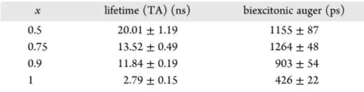
shows the dynamics of the bleaching band, and the decay traces are normalized such that their long-time scale (∼7 ns) tails are made to overlap. The average number of excitons per particle ⟨N⟩ follows a Poisson distribution, and when ⟨N⟩ equals 0.11 (Figure 3c) the probability of single exciton formation in an NPL is 20 times of that of multiexcitons, while biexcitonic processes are dominant when⟨N⟩ is 0.53. Using the method reported by Klimov et al.10(seeFigure S14), the Auger lifetime was determined for samples with different mixtures of Zn and Cd in the shell. As shown inTable 1, CdSe/Cd1−xZnxS NPLs
with alloyed shells have a longer biexciton lifetime than CdSe/ ZnS NPLs, and their Auger lifetime is maximized when x = 0.75. Interestingly, the x = 0.75 NPLs also have the highest PL quantum yield.
The confinement potential of the core/shell nanocrystals has previously been engineered to suppress the Auger process.46−48 Minimizing the high-frequency components of the Fourier
expansion of the ground-state wave function has been seen to reduce the Auger rate.46This suggests that an optimal shape of confinement potential may exist, one that minimizes the Auger process; however, this has not previously been systematically searched for using alloyed gradient composition in shells.
Wefind a non-monotonic dependence of biexcitonic Auger lifetime on the alloyed shell composition, and when x = 0.75, the Auger process is mostly mitigated by an order of magnitude compared to the sample with abrupt confinement. Similar nonmonotonic behavior of the Auger process lifetime was shown via adjusting the shell thickness.33 The concurrent achievement of the highest PLQY and longest biexciton lifetime also indicate that the trap states at the core/shell interface are best passivated when x = 0.75 because the traps not only reduce the PLQY but also induce Auger processes.49
We pursued lasing by forming a VCSEL (Figure 4c) sandwiching NPLs between two distributed Bragg reflectors (DBRs). Each DBR consists of 11 periods of alternating SiOx
and SiNxlayers. The DBRs exhibit reflectance of 96% at 660 nm and over 94% from 611 to 672 nm. Reflection and transmission spectra of our DBRs are presented inFigure 4a. A wedged cavity, made by placing a 40μm thick tape at one side, allows us to find the optimum, where the Fabry−Pérot cavity resonance overlaps the gain profile of the NPLs. In light of the strong absorption (44%) of the SiNxat wavelength 400 nm, considerable excitation power is lost as heat. We therefore pursued 2PA photoexcitation, leveraging 96% transmittance at 800 nm.
The optical gain from the x = 0.75 NPLs resides within the stop band of the DBRs, and the lasing spectrum obtained at elevated pumpfluence manifests equally spaced modes (Figure 4b), which is consistent with the resonant condition of the Fabry−Pérot cavity. Using a circular lens, we collected the VCSEL output and observed a laser spot at a distance of 60 cm. The pump-fluence-dependent device output inFigure 4d shows S-like behavior with a lasing threshold and saturation. The inset shows the single-mode lasing of our VCSEL output with a 0.61 nm fwhm. The evolution of the single-mode lasing spectrum as a function of the pumpfluence is shown inFigure S15.
CONCLUSIONS
In conclusion, via the virtue of the CdSe/CdZnS core/alloyed giant shell architecture, the HIS growth provides a convenient approach to achieve near-unity quantum yield, narrow line width, and high stability. By tuning the ratio between Zn and Cd, the shell composition is carefully adjusted to achieve an optimal confinement potential profile that allows a biexciton to achieve Auger lifetimes longer than 1 ns. As a result of the high PLQY and the well-suppressed Auger process, these CdSe/CdZnS core/alloyed g-HIS NPLs exhibit a stable and record-low threshold optical gain (2.35μJ cm−2and 0.83 mJ cm−2under one- and two-photon pumping, respectively) among the chalcogenide semiconductor nanocrystals. Using this kind of NPLs as the gain medium, efficient single-mode VCSEL is demonstrated with a threshold of 0.55 mJ cm−2 under 2PA optical pumping. Thesefindings reveal the exceptional optical gain performance of CdSe/CdZnS core/alloyed g-HIS NPLs, which makes them attractive candidates for continuous-wave colloidal lasers and even possibly electrically driven ones. METHODS
Preparation of Cd-Myristate and Synthesis of the 4 ML CdSe Core NPL. Detailed precursor preparation and 4 ML CdSe NPLs synthesis are given in theSupporting Information.
Table 1. Single Excitonic Lifetime Fits and Auger Lifetimes for the Decay of Photobleaching Band inFigure 3
x lifetime (TA) (ns) biexcitonic auger (ps)
0.5 20.01± 1.19 1155± 87
0.75 13.52± 0.49 1264± 48
0.9 11.84± 0.19 903± 54
1 2.79± 0.15 426± 22
CdSe/Cd0.25Zn0.75S Core/Alloyed g-HIS NPL Synthesis. A mixture of 11.53 mg of Cd-acetate, 27.52 mg of Zn-acetate, 0.5 mL of oleic acid, 1 mL of 4 ML CdSe core NPL in hexane, and 5 mL of 1-octadecene (ODE) was combined in a 50 mL three-neck quartzflask together with a magnetic stirrer. To remove oxygen, moisture, and hexane, theflask was kept under vacuum at room temperature for 75 min. Then the temperature of the mixture was increased to 80°C under vacuum, and at 80°C, the mixture was degassed for 45 min to form Cd-oleate and Zn-Cd-oleate and also to remove the hexane completely. Then argonflow was started through the Schlenk line, and the solution was heated up to 300°C. Degassed oleylamine (0.5 mL) was injected at 90 °C. 1-Octanethiol (70 μL) in 4 mL of ODE was used as the S-source, and the injection was started at 165°C at the rate of 10 mL per hour using a syringe pump. The injection rate was decreased to 4 mL per hour when the temperature of the solution reached 240°C and then kept at this rate until the precursor was fully injected. When the temperature reached 300°C, the solution was kept at this temperature for 50 min. Then the reaction was quenched with a water bath, and 5 mL hexane was added at 60°C. The as-synthesized core/alloyed g-HIS NPLs were precipitated by adding 5 mL of ethanol, and the precipitated NPLs were redispersed in hexane or toluene.
ASSOCIATED CONTENT
*
S Supporting InformationThe Supporting Information is available free of charge on the
ACS Publications websiteat DOI:10.1021/acsnano.9b04967.
Chemicals, preparation of the Cd-myristate, 4 ML CdSe core NPL synthesis, characterization, cross-sectional HRTEM of the synthesized core/g-HIS NPL image, HAADF-STEM images of CdSe/Cd1−xZnxS core/alloyed
g-HIS NPLs using the tuned values of x composition, effect of the injection temperature of the S-precursor on the PL of synthesized core/alloyed g-HIS NPLs, optical properties of reproducible synthesis of CdSe/ Cd0.25Zn0.75S core/alloyed g-HIS NPL samples,
cross-sectional TEM images of the synthesized CdSe/ Cd0.25Zn0.75S core/alloyed g-HIS NPLs, TEM images
and EDX analyses of the synthesized CdSe/Cd0.75Zn0.25S
core/alloyed g-HIS NPLs, XPS spectra of the CdSe/ Cd1−xZnxS core/alloyed g-HIS NPLs samples for all
compositions, atomic ratios of Zn and Cd elements in the structure of the core/alloyed g-HIS NPLs from XPS and EDX analyses, atomic ratios of the elements (given in %) with respect to different shells, amplified spontaneous emission (ASE) peak intensity under constant optical pumping under 1PA for x = 0.75 and x = 1, variation in the emission spectra of CdSe/Cd0.25Zn0.75S core/alloyed
g-HIS NPLs as a function of the pumpfluence under 355 nm Nd:YAG laser pumping, determination of the average number of electron and hole pairs, and determination of
Figure 4. (a) Spectral transmittance (dashed line) and reflectance (solid line) of the distributed Bragg reflectors that were used in our laser cavity. The lasing modes of NPLs havingx = 0.75 shell composition under 2PA excitation reside within the stop band of the DBR mirrors. (b) Positions and fwhm’s (with error bars) of the lasing modes of the spectrum given in (a). (c) Photograph of the colloidal lasing set up and laser beam spot observed at a distance of 60 cm from the laser cavity (Bilkent University logo used with permission). The inset shows the lasing peak spectrum with a 0.61 nm fwhm. (d) Pump-fluence-dependent emission intensity of single-mode NPL lasing shows S-curve characteristics. fwhm of the emission narrowed down to 0.61 nm after the laser action took place.
the Auger lifetime of (a) x = 0.50, (b) x = 0.75, (c) x = 0.90, and (d) x = 1.00 CdSe/Cd1−xZnxS core/alloyed
g-HIS NPLs (PDF) AUTHOR INFORMATION
Corresponding Authors
*E-mail:[email protected],[email protected]. *E-mail:[email protected]. *E-mail:[email protected]. ORCID Yuan Gao:0000-0001-9407-1528 Evren Mutlugun:0000-0003-3715-5594 Edward H. Sargent:0000-0003-0396-6495
Hilmi Volkan Demir:0000-0003-1793-112X Author Contributions
⊥Y.A., K.G., and Y.G. contributed equally.
Notes
The authors declare no competingfinancial interest. ACKNOWLEDGMENTS
The authors gratefully acknowledgefinancial support from the Singapore National Research Foundation under the programs of NRF-NRFI2016-08 and the Science and Engineering Research Council, Agency for Science, Technology and Research (A*STAR) of Singapore and also partially from TUBITAK 115E679 and 117E713. H.V.D. acknowledges support from TUBA. E.M. acknowledges support from TUBA-GEBIP, and E.M. and Y.A. also acknowledge funding from Abdullah Gul University Scientific Research Project No. FDK-2017-96. K.G. and M.S. acknowledge support from TUBITAK BIDEB 2211 program. We further acknowledge Mr. Mustafa Guler for his assistance in TEM imaging.
REFERENCES
(1) Lhuillier, E.; Pedetti, S.; Ithurria, S.; Nadal, B.; Heuclin, H.; Dubertret, B. Two-Dimensional Colloidal Metal Chalcogenides Semiconductors: Synthesis, Spectroscopy, and Applications. Acc. Chem. Res. 2015, 48, 22−30.
(2) Kovalenko, M. V.; Manna, L.; Cabot, A.; Hens, Z.; Talapin, D. V.; Kagan, C. R.; Klimov, V. I.; Rogach, A. L.; Reiss, P.; Milliron, D. J.; Guyot-Sionnnest, P.; Konstantatos, G.; Parak, W. J.; Hyeon, T.; Korgel, B. A.; Murray, C. B.; Heiss, W. Prospects of Nanoscience with Nanocrystals. ACS Nano 2015, 9, 1012−1057.
(3) Ithurria, S.; Tessier, M. D.; Mahler, B.; Lobo, R. P. S. M.; Dubertret, B.; Efros, A. L. Colloidal Nanoplatelets with Two-Dimensional Electronic Structure. Nat. Mater. 2011, 10, 936−941.
(4) She, C.; Fedin, I.; Dolzhnikov, D. S.; Dahlberg, P. D.; Engel, G. S.; Schaller, R. D.; Talapin, D. V. Red, Yellow, Green, and Blue Amplified Spontaneous Emission and Lasing Using Colloidal CdSe Nano-platelets. ACS Nano 2015, 9, 9475−9485.
(5) Gao, Y.; Li, M.; Delikanli, S.; Zheng, H.; Liu, B.; Dang, C.; Sum, T. C.; Demir, H. V. Low-Threshold Lasing from Colloidal CdSe/CdSeTe Core/Alloyed-Crown Type-II Heteronanoplatelets. Nanoscale 2018, 10, 9466−9475.
(6) Liu, B.; Delikanli, S.; Gao, Y.; Dede, D.; Gungor, K.; Demir, H. V. Nanocrystal Light-Emitting Diodes Based on Type II Nanoplatelets. Nano Energy 2018, 47, 115−122.
(7) Luo, S.; Kazes, M.; Lin, H.; Oron, D. Strain-Induced Type II Band Alignment Control in CdSe Nanoplatelet/ZnS-Sensitized Solar Cells. J. Phys. Chem. C 2017, 121, 11136−11143.
(8) Lhuillier, E.; Robin, A.; Ithurria, S.; Aubin, H.; Dubertret, B. Electrolyte-Gated Colloidal Nanoplatelets-Based Phototransistor and Its Use for Bicolor Detection. Nano Lett. 2014, 14, 2715−2719.
(9) Pelton, M. Carrier Dynamics, Optical Gain, and Lasing with Colloidal Quantum Wells. J. Phys. Chem. C 2018, 122, 10659−10674. (10) Klimov, V. I.; Mikhailovsky, A. A.; McBranch, D. W.; Leatherdale, C. A.; Bawendi, M. G. Quantization of Multiparticle Auger Rates in Semiconductor Quantum Dots. Science 2000, 287, 1011−1014.
(11) Grim, J. Q.; Christodoulou, S.; Di Stasio, F.; Krahne, R.; Cingolani, R.; Manna, L.; Moreels, I. Continuous-Wave Biexciton Lasing at Room Temperature Using Solution-Processed Quantum Wells. Nat. Nanotechnol. 2014, 9, 891−895.
(12) Guzelturk, B.; Kelestemur, Y.; Olutas, M.; Delikanli, S.; Demir, H. V. Amplified Spontaneous Emission and Lasing in Colloidal Nanoplatelets. ACS Nano 2014, 8, 6599−6605.
(13) Baghani, E.; O'Leary, S. K.; Fedin, I.; Talapin, D. V.; Pelton, M. Auger-Limited Carrier Recombination and Relaxation in CdSe Colloidal Quantum Wells. J. Phys. Chem. Lett. 2015, 6, 1032−1036.
(14) Ma, X.; Diroll, B. T.; Cho, W.; Fedin, I.; Schaller, R. D.; Talapin, D. V.; Gray, S. K.; Wiederrecht, G. P.; Gosztola, D. J. Size-Dependent Biexciton Quantum Yields and Carrier Dynamics of Quasi-Two-Dimensional Core/Shell Nanoplatelets. ACS Nano 2017, 11, 9119− 9127.
(15) Li, M.; Zhi, M.; Zhu, H.; Wu, W.-Y.; Xu, Q.-H.; Jhon, M. H.; Chan, Y. Ultralow-Threshold Multiphoton-Pumped Lasing from Colloidal Nanoplatelets in Solution. Nat. Commun. 2015, 6, 8513.
(16) Yang, Z.; Pelton, M.; Fedin, I.; Talapin, D. V.; Waks, E. A Room Temperature Continuous-Wave Nanolaser Using Colloidal Quantum Wells. Nat. Commun. 2017, 8, 143.
(17) Ithurria, S.; Talapin, D. V. Colloidal Atomic Layer Deposition (c-ALD) Using Self-Limiting Reactions at Nanocrystal Surface Coupled to Phase Transfer between Polar and Nonpolar Media. J. Am. Chem. Soc. 2012, 134, 18585−18590.
(18) Jana, S.; Phan, T. N. T.; Bouet, C.; Tessier, M. D.; Davidson, P.; Dubertret, B.; Abécassis, B. Stacking and Colloidal Stability of CdSe Nanoplatelets. Langmuir 2015, 31, 10532−10539.
(19) Abécassis, B.; Tessier, M. D.; Davidson, P.; Dubertret, B. Self-Assembly of CdSe Nanoplatelets into Giant Micrometer-Scale Needles Emitting Polarized Light. Nano Lett. 2014, 14, 710−715.
(20) Kelestemur, Y.; Guzelturk, B.; Erdem, O.; Olutas, M.; Gungor, K.; Demir, H. V. Platelet-in-Box Colloidal Quantum Wells: CdSe/ CdS@CdS Core/Crown@Shell Heteronanoplatelets. Adv. Funct. Mater. 2016, 26, 3570−3579.
(21) Tessier, M. D.; Spinicelli, P.; Dupont, D.; Patriarche, G.; Ithurria, S.; Dubertret, B. Efficient Exciton Concentrators Built from Colloidal Core/Crown CdSe/CdS Semiconductor Nanoplatelets. Nano Lett. 2014, 14, 207−213.
(22) Prudnikau, A.; Chuvilin, A.; Artemyev, M. CdSe−CdS Nanoheteroplatelets with Efficient Photoexcitation of Central CdSe Region through Epitaxially Grown CdS Wings. J. Am. Chem. Soc. 2013, 135, 14476−14479.
(23) Pedetti, S.; Ithurria, S.; Heuclin, H.; Patriarche, G.; Dubertret, B. Type-II CdSe/CdTe Core/Crown Semiconductor Nanoplatelets. J. Am. Chem. Soc. 2014, 136, 16430−16438.
(24) Kelestemur, Y.; Olutas, M.; Delikanli, S.; Guzelturk, B.; Akgul, M. Z.; Demir, H. V. Type-II Colloidal Quantum Wells: CdSe/CdTe Core/ Crown Heteronanoplatelets. J. Phys. Chem. C 2015, 119, 2177−2185. (25) Kelestemur, Y.; Guzelturk, B.; Erdem, O.; Olutas, M.; Erdem, T.; Usanmaz, C. F.; Gungor, K.; Demir, H. V. CdSe/CdSe 1− x Te x Core/ Crown Heteronanoplatelets: Tuning the Excitonic Properties without Changing the Thickness. J. Phys. Chem. C 2017, 121, 4650−4658.
(26) Mahler, B.; Nadal, B.; Bouet, C.; Patriarche, G.; Dubertret, B. Core/Shell Colloidal Semiconductor Nanoplatelets. J. Am. Chem. Soc. 2012, 134, 18591−18598.
(27) Rossinelli, A. A.; Riedinger, A.; Marqués-Gallego, P.; Knüsel, P. N.; Antolinez, F. V.; Norris, D. J. High-Temperature Growth of Thick-Shell CdSe/CdS Core/Thick-Shell Nanoplatelets. Chem. Commun. 2017, 53, 9938−9941.
(28) Polovitsyn, A.; Dang, Z.; Movilla, J. L.; Martín-García, B.; Khan, A. H.; Bertrand, G. H. V.; Brescia, R.; Moreels, I. Synthesis of Air-Stable
CdSe/ZnS Core-Shell Nanoplatelets with Tunable Emission Wave-length. Chem. Mater. 2017, 29, 5671−5680.
(29) Cruguel, H.; Livache, C.; Martinez, B.; Pedetti, S.; Pierucci, D.; Izquierdo, E.; Dufour, M.; Ithurria, S.; Aubin, H.; Ouerghi, A.; Lacaze, E.; Silly, M. G.; Dubertret, B.; Lhuillier, E. Electronic Structure of CdSe-ZnS 2D Nanoplatelets. Appl. Phys. Lett. 2017, 110, 152103.
(30) Shendre, S.; Delikanli, S.; Li, M.; Dede, D.; Pan, Z.; Ha, S. T.; Fu, Y. H.; Hernandez Martinez, P. L.; Yu, J.; Erdem, O.; Kuznetsov, A. I.; Dang, C.; Sum, T. C.; Demir, H. V. Ultrahigh-Efficiency Aqueous Flat Nanocrystals of CdSe/CdS@Cd 1-x Zn x S Colloidal Core/Crown@ Alloyed-Shell Quantum Wells. Nanoscale 2019, 11, 301−310.
(31) Tessier, M. D.; Mahler, B.; Nadal, B.; Heuclin, H.; Pedetti, S.; Dubertret, B. Spectroscopy of Colloidal Semiconductor Core/Shell Nanoplatelets with High Quantum Yield. Nano Lett. 2013, 13, 3321− 3328.
(32) Altintas, Y.; Gungor, K.; Quliyeva, U.; Erdem, O.; Kelestemur, Y.; Mutlugun, E.; Kovalenko, M. V.; Demir, H. V. Highly Stable, Near-Unity Efficiency Atomically Flat Semiconductor Nanocrystals of CdSe/ ZnS Hetero-Nanoplatelets Enabled by ZnS-Shell Hot-Injection Growth. Small 2019, 15, 1804854.
(33) Pelton, M.; Andrews, J. J.; Fedin, I.; Talapin, D. V.; Leng, H.; O’Leary, S. K. Nonmonotonic Dependence of Auger Recombination Rate on Shell Thickness for CdSe/CdS Core/Shell Nanoplatelets. Nano Lett. 2017, 17, 6900−6906.
(34) Park, Y.-S.; Lim, J.; Klimov, V. I. Asymmetrically Strained Quantum Dots with Non-Fluctuating Single-Dot Emission Spectra and Subthermal Room-Temperature Linewidths. Nat. Mater. 2019, 18, 249−255.
(35) She, C.; Fedin, I.; Dolzhnikov, D. S.; Demortière, A.; Schaller, R. D.; Pelton, M.; Talapin, D. V. Low-Threshold Stimulated Emission Using Colloidal Quantum Wells. Nano Lett. 2014, 14, 2772−2777.
(36) Wang, Y.; Zhi, M.; Chang, Y. Q.; Zhang, J. P.; Chan, Y. Ultralow Threshold Amplified Spontaneous Emission from CsPbBr3 Nano-particles Exhibiting Trion Gain. Nano Lett. 2018, 18, 4976−4984.
(37) Akkerman, Q. A.; D’Innocenzo, V.; Accornero, S.; Scarpellini, A.; Petrozza, A.; Prato, M.; Manna, L. Tuning the Optical Properties of Cesium Lead Halide Perovskite Nanocrystals by Anion Exchange Reactions. J. Am. Chem. Soc. 2015, 137, 10276−10281.
(38) Bischak, C. G.; Hetherington, C. L.; Wu, H.; Aloni, S.; Ogletree, D. F.; Limmer, D. T.; Ginsberg, N. S. Origin of Reversible Photoinduced Phase Separation in Hybrid Perovskites. Nano Lett. 2017, 17, 1028−1033.
(39) Cui, J.; Beyler, A. P.; Coropceanu, I.; Cleary, L.; Avila, T. R.; Chen, Y.; Cordero, J. M.; Heathcote, S. L.; Harris, D. K.; Chen, O.; Cao, J.; Bawendi, M. G. Evolution of the Single-Nanocrystal Photo-luminescence Linewidth with Size and Shell: Implications for Exciton-Phonon Coupling and the Optimization of Spectral Line-widths. Nano Lett. 2016, 16, 289−296.
(40) de Mello, J. C.; Wittmann, H. F.; Friend, R. H. An Improved Experimental Determination of External Photoluminescence Quantum Efficiency. Adv. Mater. 1997, 9, 230−232.
(41) Park, Y. S.; Bae, W. K.; Baker, T.; Lim, J.; Klimov, V. I. Effect of Auger Recombination on Lasing in Heterostructured Quantum Dots with Engineered Core/Shell Interfaces. Nano Lett. 2015, 15, 7319− 7328.
(42) Li, Q.; Lian, T. Area- and Thickness-Dependent Biexciton Auger Recombination in Colloidal CdSe Nanoplatelets: Breaking the Universal Volume Scaling Law. Nano Lett. 2017, 17, 3152−3158.
(43) Klimov, V. I.; Mikhailovsky, A. A.; Xu, S.; Malko, A.; Hollingsworth, J. A.; Leatherdale, C. A.; Eisler, H.-J.; Bawendi, M. G. Optical Gain and Stimulated Emission in Nanocrystal Quantum Dots. Science 2000, 290, 314−317.
(44) Klimov, V. I.; Ivanov, S. A.; Nanda, J.; Achermann, M.; Bezel, I.; McGuire, J. A.; Piryatinski, A. Single-Exciton Optical Gain in Semiconductor Nanocrystals. Nature 2007, 447, 441−446.
(45) Li, M.; Bhaumik, S.; Goh, T. W.; Kumar, M. S.; Yantara, N.; Grätzel, M.; Mhaisalkar, S.; Mathews, N.; Sum, T. C. Slow Cooling and Highly Efficient Extraction of Hot Carriers in Colloidal Perovskite Nanocrystals. Nat. Commun. 2017, 8, 14350.
(46) Cragg, G. E.; Efros, A. L. Suppression of Auger Processes in Confined Structures. Nano Lett. 2010, 10, 313−317.
(47) Vaxenburg, R.; Rodina, A.; Lifshitz, E.; Efros, A. L. Biexciton Auger Recombination in CdSe/CdS Core/Shell Semiconductor Nanocrystals. Nano Lett. 2016, 16, 2503−2511.
(48) Bae, W. K.; Padilha, L. A.; Park, Y.-S.; McDaniel, H.; Robel, I.; Pietryga, J. M.; Klimov, V. I. Controlled Alloying of the Core−Shell Interface in CdSe/CdS Quantum Dots for Suppression of Auger Recombination. ACS Nano 2013, 7, 3411−3419.
(49) Beane, G. A.; Gong, K.; Kelley, D. F. Auger and Carrier Trapping Dynamics in Core/Shell Quantum Dots Having Sharp and Alloyed Interfaces. ACS Nano 2016, 10, 3755−3765.