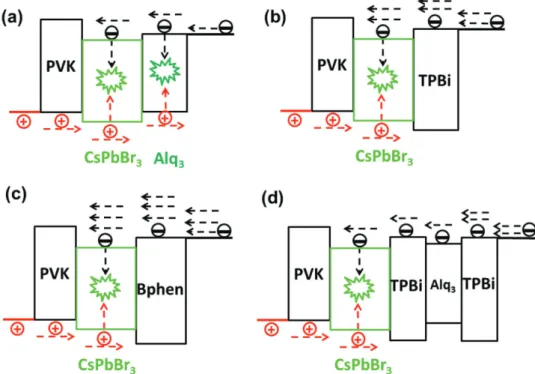
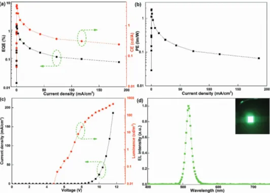
Highly efficient green light-emitting diodes from all-inorganic perovskite nanocrystals enabled by a new electron transport layer
Tam metin
Şekil

Benzer Belgeler
Meriv wexta ku xwe berdide nava helbestê dibîne ku nîgaşên xweş bi kar anîne. A yekem devê xwe dişibîne şikeftê. Şikeft pi piranî cihên kesên ku jiyana xwe bi
and sufficient conditions for the controllability of conewise linear systems,” IEEE Transactions on Automatic Control, vol. Shen, “Conewise linear systems: non-zenoness
The net-cut size of a cell-cluster that will be induced by the node-cluster to be formed upon selecting a node in G will be referred here as the valence of that
It is possible to obtain either exact realizations or useful approximations of linear systems or matrk-vector prod- ucts arising in many different applications, by synthesiz-
The lone pairs of electrons for nitrogen, oxygen, and fluorine atoms make them proper sites for detection of changes to electronic dis- tributions by indirect effects of HB
It can be noted that the highest imported sources of effective- taxes, at around 6% of purchaser prices, is observed for Manufacture of Land Transport Vehicles
In Chapter 4, we compute the kernels of various bounded linear functionals and Bergman projections of certain functions related to them.. In Chapter 5, we solve a few
The projected band diagram is a complicated way to explain the omnidirec- tional reflectivity inside transmission bragg fibers. In order to clarify the picture we prefer to use an
