* Лі-гі.· i i W£ ·* -wi I Ír¿ .jlA ¿ ¿Vl'i O'F »*îw.* w .w ^. i i w>/: СГГ. WiXr- w i /
·^i i ATV СЫ W Δ ir-5іГ С í***U
к\-^А^ А 4 Ѵ*^ѵ^» rf і 4 ·! «·* aw . ¿‘W· 2ÏW WWw ¿'w ¿ I t'\ í w " ' r*^· !'>ta» ϊ,^ ί^ ·., '* “ .. «^ ,*-·* - * · f » .; í .·; , .■ y ;. . '. .1 ·'* · '-Чс·.. • 4 « ·<«!# · 4*í> «л*»ѵ i ' . ^ 4* . / 4e*í ·|^ ' i ' " - Ä w л Α Λ ? ^ · ■ : і ^ . ; - ' ’Г Г ' · . . . ' “ * f ί · ; α *iíl^ j, >;;^ 4 r^X ΔVO . -b·^ 4W . **’ : ? ► i - i . ■,·*·■. · ·■■ 5/ '.■f · ' ; Ï** * ? '' I v i í ^ H ··^ · * ,· ^ r « i гчЧ' J ::. '••'í·· . , ·*··.·%■■;:■ í .·· ч2 / '· '■ < «. a' J *M · » · '♦ 'W ' Ä » *■ « M » V ii·' V «o*'*·*' W ·''♦ Г * ‘^в*»ч*1* ‘ ь V '.· 4' ■'.·*^· ·....' .j1>W·, . ■.' J i i y _,''t^ - ΐϋ 'iXíSí/^r a· M . a— 'а Ч ,» * ..· .•’лЛтМ^·, « * W << 'W<*- W w«4 .. »''4^ » Ч ■ri-s-VO^wV' ;'. . -,«;·'■ r-"" ·'“?;'
lÉBi
FABRICATION AND CHARACTERIZATION OF
HIGITSPEED, HIGH QUANTUM EFFICIENCY,
RESONANT CAVITY ENHANCED SCHOTTKY
PHOTODIODES
A THESIS
SUBMITTED TO THE DEPARTMENT OF PHYSICS AND THE INSTITUTE OF ENGINEERING AND SCIENCE
OF BILKENT UNIVERSITY
IN PARTIAL FULFILLMENT OF THE REQUIREMENTS FOR THE DEGREE OF
DOCTOR OF PHILOSOPHY
By
Erliaii Polatkciri Ata
10 July 1998
■S3 T
Ag3
I certify that I have read this thesis and thiit in rny opinion it is fully adequate, in scope and in quality, as a dissertation for the degree of Doctor of Philosophy.
Assoc. Prof. Ekniel^izbay (Supervisor)
I certify that I have read this thesis and that in rny opinion it is fully adequate, in scope and in qucvlity, as a. dissertatioir for the degree of Doctor of Philosophy.
Assoc gdein Ergelebi
I certify that I have read this thesis and that in niy opinion it is fully adequcite, in scope and in quality, as a. dissertation for the degree of Doctor of Philosophy.
I certify that I have rccicl this thesis and that in my opinion it is fully adequate, in scope and in qucility, as a dissertation for the degree of Doctor of Philosophy.
Assoc. Prof. Orhan Aytür
I certify that I have read this thesis and that in my opinion it is fully adequate, in scope and in quality,'as a dissertation for the degree of Doctor of Philosophy.
Approved for the Institute of Engineering and Science:
<r
0 · ^
Prof. Mehmet Baray, f.
A bstract
FABRICATION AND CHARACTERIZATION OF
HIGH-SPEED, HIGH QUANTUM EFFICIENCY, RESONANT
CAVITY ENHANCED SCHOTTKY PHOTODIODES
Erhan Polatkan Ata
Ph. D. in Physics
Supervisor: Assoc. Prof. Ekmel Ozba)^
10 July 1998
Rapidly developing “photonics” technology promises higher bcindwidths of communiccition than any other techniciue did ever. The increasing rate of communication not only alters science and technology, but brings a global cultural exchange, which seems to be one of the most important revolutions in the history.
Photodetectors, as vital corniDonents of optoelectronics, cire still being developed to achieve satisfying performances for the increasing communication demcinds. We have designed and fabricated high-speed, high efficiency resonant Ccivity enhanced (RCE) Schottky photodiodes, suitable for 800-850 mil operation wavelengths. We have used two different GaAs/AlGaAs based epitaxial structures to achieve high performance. From one of these structures, we fabricated photodiodes with 50% quantum efficiency and 80 GHz 3-dB bandwidth. The other structure had a design suitable for préfabrication wavelength tuning and adjustable active layer thickness. On this structure, we achieved 20% quantum efficiency along with, world record for RGB photodiodes, over 110 (Hlz 3-dB estimated bandwidth.
We investigated effects of active layer, top Au layer, and silicon nitride coating layer thicknesses on the RCE devices. Discrepancy between theory and experiments were also explained briefly.
Methods for improving performances of photodiodes has been proposed ¿is possible future work. Possible appliccitions, which may make use of current know how on the subject, have also been mentioned.
Keywords: Resomuit Ckivity, Resonant Cavity Enhcuicement, Photodiode, Schottky Contfxct, Schottky Photodiode, Quantum Efficiency, High-Speed.
ö z e t
RESONANT KAVITE ILE GÜÇLENDİRİLMİŞ, YÜKSEK
HIZLI VE YÜKSEK VERİMLİ, SCHOTTKY FOTODİYOT
ÜRETİMİ VE KARAKTERİZASYONU
Erhan Polatkarı Ata
Fizik Doktora
Tez Yöneticisi: Doç. Dr. Ekmel Ozbciy
10 Temmuz 1998
Hızla gelişen “photoriics” teknolojisi, diğer teknolo jilerin vaadetmiş olduğundan dciha yüksek bcint genişlikleri vaadetmektedir. Artan iletişim, sadece bilim ve teknolojiyi geliştirmekle kalmayıp, aynı zamanda tarihteki en önemli devrimler- den birini, küresel kültür alışverişini sağlamaktadır.
Optolektroniğin yaşamsal elemanlarından olan fotodetektörler, artan iletişim talebini karşıhıyabilecek perlörmanslara ıılcişabilmek için hala geliştirilmektedir. 800-850 nrn dalgaboyları için yüksek verimli ve yüksek hızlı, rezonant kcivite ile güçlendirilmiş (RCE) Schottky fotodiyotlar tasarladık ve ürettik. Yüksek performans elde ettiğimiz GaAs/AlGaAs temelli iki ayrı yapı kullandık. Bu yapılardan birisinden verimlilikleri %50, 3-dB bant genişlikleri de 80 GHz olan fotodiyotlar ürettik, öteki yapının tasarımı üretim öncesi dalgaboyu ve aktif katman kalınlık ayarı yapmaya uygun idi. Bu yapı üzerinde %20 kuvanturn verimliliği ve RGE fotodijmtlar için dünya rekoru olan, 110 GHz öngörülen 3- dB bant genişliği elde ettik.
Aktif katmanın, yüzeydeki Au katmanının ve silikon nitrat katmalımın m
kalınlıklarınm RCE ciygıtlcir üzerindeki etkilerini de inceledik. Aynı zamanda, teori ve deney arasındaki farklılıkları da kısaca açıkladık.
Fotodiyotların performanslarını arttırmaya yönelik teknikler, olası gelecek çalışması olarak önerdik. Ayrıca, konu ile ilgili edindiğimiz tecrübenin kullanılabileceği olası uygulamalara da değindik.
Analıtar Sözcükler: Rezonant Kavite, Rezonant Kavite İle Güçlendir Fotodiyot, Scliottky Eklemi, Kuvantum Verimliliği, Yüksek Hız.
A cknow ledgem ent s
It is iny plc'asure to ('xpress 1113^ ileepest gratitude' lo my supervisor Ekniel ()/J)a.y for his invaluahh' guidaiice', motivation, morale siij^iport, and patience dui-iiig my graduai(' study.
I wish to thank tlu' past and |)resent memljers ot tlie |)liysics department, without whom this study would not he possible. Especially, t.lie members of Adva.nced Resea.rcli Laboratories, wlio (somehow) luanaged to turn hard times into ('iijoyable ones.
1 wish to a.ddress iuva.liuil)le helps and liospita.lity of M. Seliin Ünlü and his graduate students during my visit to Eicose'cond Ija.boratory at l^hotonics (k'liter
n\‘ Boston University.
1 wish to thank the UK'inbers of my proposal and Ph. D. defense committee, (or tİK'ir helpful guidance and constructive criticisms.
I am in debt to my Family and friends for tlieir sii|)|)oi‘ts and i)a.l,ience. Without tliem, I would not b(' who 1 am.
Sa.va,thanks lor thos(' who liave inade music for me, a.nd reminded that “ in tlie dai'k, it is easier to see'."’
The precious one who loves me and wliom 1 lovc'; you give' nu' everything I ii('('d.
C ontents
A bstract
Ozet 111
Acknow ledgem ents
Contents VI
List of Figures List of Tables
vin
1 Introduction
1.1 Why Schottky Photodiodes?... 1.2 Why Resonant Cavity Enlmncement? 1.3 RCE Schottky Photodiode Research .
1 2 3 4 2 T heory 6 2.1 The P ho to d io d e... 6 2.2 Metal-Seiriiconductor P h o to d io d e ... 7
2.3 Carrier Transport and Speed L im itatio n s... 10
2.4 RC time c o n s ta n t... 11
2.5 Puise response... 11
2.6 Dillusion current 12
2.7 Carrier Trapping 12
2.8 Quantum Eiiiciency of a Metal-Semiconductor Photodiode . . . . 13
2.9 Resonant Ccivity Enhcincement... 14
3 Fabrication 23 3.1 Sample Prepa.ration and C lea n in g ... 23
3.2 Pliotolitliography... 25 3.2.1 Image-reversai tec h n iq u e ... 26 3.3 M etalization... 27 3.4 Wet Chemical E tc h in g ... 28 3.5 Dielectric C o atin g ... 28 3.6 Photodiode Fabrication P r o c e s s ... 29 3.7 I-V T e s ts... 30 4 M easurem ents 36 4.1 Reflection Spectra of Bare S a m p le s ... 36
4.1.1 NIST sa m p le s... 37
4.1.2 ISU sam p les... 38
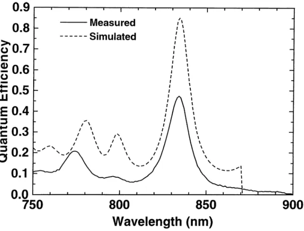
4.2 Effects of Schottky Contact and Silicon Nitride 39 4.3 Photoresponse Measurements 43 4.3.1 NIST s a m p l e ... 44
4.3.2 ISU s a m p l e ... 45
4.3.3 Surface roughness p ro b lem ... 47
4.3.4 Bias dependence 47 4.4 High Speed M easurem ents... 48
4.4.1 NIST pulse re s p o n s e ... 49
4.4.2 ISU pulse re s p o n s e ... 50
5 D iscussions and Future D irections 57
Bibliography 60
List o f Figures
2.1 A schematic diagrcirn of an illuminated Schottky junction. 8
2.2 Biased Scliottky photodiode and electric field distributions . . . . 18
2.3 Photocurrent under illumination... 19
2.4 Simplified equivalent circuit of a Schottky photodiode. 20 2.5 Schematic diagram illustrating RCE effect... 21
2.6 Wavelength dependence of quantum efficiency... 22
3.1 SEM photo showing Au deposited on image-reversed resist line. . 31
3.2 SEM photo showing Au deposited on image-reversed dot-shaped resist... 31
3.3 Schematic cross section of a fabricated RCE photodiode... 32
3.4 Microphotograph of a fabricated d e v ic e ... 33
3.5 A microphotograph of another type of a fabricated device... 34
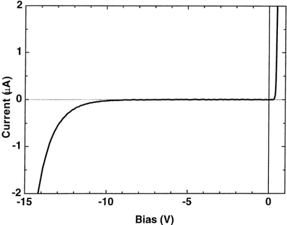
3.6 A typical I-V c u r v e ... 35
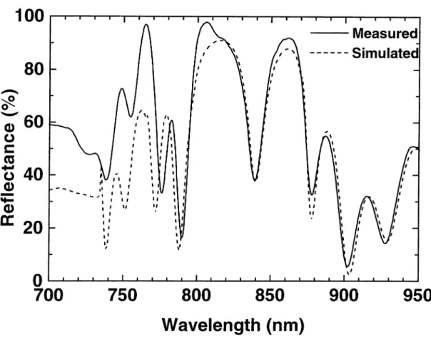
4.1 Measured and simulated reflection spectra of the NIST sample. . . 37
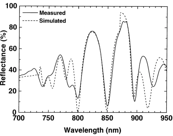
4.2 Measured and simulated reflection si^ectra of the ISU sample. 39 4.3 A set of reflection spectra of the ISU scunple... 40
4.4 A set of reflection spectra of the ISU sample with overlaying thin films... 41
4.5 Simulated reflection spectra of the ISU sample with various films. 42 4.6 A schematic diiigram of quantum efficiency measurement setup. 43 4.7 Measured and simulated photoresponses of the NIST sample. . . . 44
4.8 Measured and simulated photoresponses of the ISU Scimple . . . . 45
4.9 Measured photoresponses of the SI, S2, and S3 sam p les... 46
4.10 AFM image of 15 nm An film evaporated on GaAs... 48
4.11 AFM image of 10 nm Au film evaporated on GaAs... 49
4.12 Bias dependence of the photoresponse of the NIST scimple... 50
4.13 A schematic diagrcun af the high speed measurement setup... 51
4.14 Pulse response of the NIST sample... 52
4.15 Experimented and theoretical Bode plots for the NIST sample. . . 53
4.16 Pulse response of the ISU sample... 54
4.17 Experimental and theoretical Bode plots for the S2 scunple... 55 4.18 Theoretical Bode plots for the SI, S2, and S3 samples. 56
List o f Tables
3.1 Structure of the NIST ,s 3.2 Structure of the ISU sample
24 24
C hapter 1
Introduction
Light has always Ixeen an important medium of communication, even in prehistoric ciges. An interesting example, from the historic ¿iges of course, is the cornmuniccition of the fcill of Troy to Queen Clytemnestra in 1184 B. C., by a series of line of sight beacons of fires covering 900 km! Until scientists and researchers discovered light-material interactions (and vice versa), such as Nobel Prize awcirded discovery of photo-electric effect by Albert Einstein, cind developed methods to create, guide, and detect light; the only light sources, for communications, were heavenly bodies and fire. The guides were simple optical lenses and mirrors, and sensors were human eyes. The first two components, namely sources and guides, has always meant some level of technology, existed for centuries. The third, detection, has been performed by human eye until last few decades. Today, information systems use light without any need for a human eye, well, at least at some intermediate stages! This has been possible by developments in tlie fields of light generation (like lasers), transfer (like optical fibers), and detection (like photodetectors), “photonics” in short. In this work we studied some aspects of the light detection, photodetection, on a class of photodetectors, namely photodiodes.
Although the above paragraph is about optical communications, photode tectors find applications in many fields of science and technology, with an increcising rate and broadening range of applications. Photodiodes are vital
components of optoelectronic systems, which explains the importance of maturing their performances. Our work covers experimental study of a specific family of photodiodes, namely resonant cavity enhanced (RCE) Schottky photodiodes, supported by theoretical computer simulations.
Chapter 1. Introduction 2
1.1
W h y S ch ottk y P h o to d io d es?
Surprisingly, knowledge on Schottky contacts is mciybe older thcin Schottky himself. More tha,n a hundred years ago work of Braun in 1874,^ showed the asymmetric nature of electrical conduction of metal contacts on semiconductors, such as copper on iron sulphide. First point contact detector patent was taken in 1906 by Pickard.^ Although technologically oldest of semiconductor electronic components, the understanding of rectification mechanism took long decades of studies, both experimental and theoreticcil, of famous names, Schottky, Mott, Davydov, Bethe, Bcirdeen, Crowell, Sze, Mead, and many others. Even though working models and theories have been developed, a full physical understanding and prediction of Schottky contacts, especially on ÍII-V materials, are still not as developed as for many of the other semiconductor devices. The reader is referred to the book by Rhoderick and Williams^ for detailed information on metal-semiconductor j unctions.
The advantages of Schottky diodes are their simplicity, ecvsily obtainable compatibility with idmost any microelectronics fabrication process, and excellent high sjDeed performances. Schottky barrier diode being a majority carrier device, does not suffer from response delays arising from the minority carrier diffusion issues, which ex|)lains its multi-terahertz high-speed performance. As will be explained in section 2.3, speed limitations of a Schottky photodiode depends on carrier transit time and RC time constant, which can be kept small with ease compared to other types of photodiodes by a careful design of a Schottky device.
Applications in terahertz regime include mixers,'*’® detectors,** and harmonic multipliers.^ To our knowledge, first use of a rnetal-semiconductor diode as a high- efficiency photodetector is made by Ahlstrom et. al. and Schneider.**’** Since then.
Chapter 1. Introduction
3-clB bcindwidths in excess of 100 GHz discrete^"’^^ and rnonolithically integrated devices^^ have been reported.
1.2
W h y R eson an t C avity E nhan cem en t?
The modern society demands almost unlimited communication, which requires systems with extreme capacity performances. Optical fibers have telecommuni- Ccition bandwidths about 25 THz, which is three orders of magnitude larger as compared to present optoelectronic systems with ojDerating capcicities less than 10 gigabits pon: second. Present microelectronics technology is not capable to increase bandwidth of electronic systems to such high values. However, similar to parallel processing in computers, we can use a larger fraction of the fiber capacity by means of parallel communication channels through optical fibers. The realization of parallel channels is possible by the technique known cis wavelength division multiplexing (WDM), in which up to 500 different wavelength optical signals can be trcinsrnitted through a single fiber.
Resonant cavity enhanced (RCE) photodetectors hcive the advantciges of both wavelength selectivity and high quantum efficiency, without any sacrifice of high speed performance.^^ Although fundamental physics of resoucint cavities has been known for more than a hundred 3'^ears, their implementation to optoelectronics beccime a hot topic in early 1990s.
Recent accomplishments by means of RCE effect can be summarized as follows. Avalanche photodetectors (APDs) with 75 % peak external quantum efficiencies,low gciin bandwidth of 33 GHz, and gain-bcindwidth product of 290 GHz^·^ were fabricated by a group at University of Texas at Austin. The same group made use of a 1 /tin thick polysilicon absorption layer combined with Si-SiO'i Bragg reflectors to obtain 44% qucintum efficiency and bandwidth >1.4 GRzd^ Inti’cicavity re.sonant quantum well photodetectors embedded in vertical cavity surface emitting laser (VCSEL) structures were demonstrated at UC Berkeley. These detectors were intended as feedback devices tor VGSELs fabricated and yielded the required low sensitivity to spontaneous emission cincl
high effective responsivity for the first time in such an appiiccition.^’^ The same group also fa.bricatecl 30 rirri wide and continuously tunable RCE photodetectors, that can also operate in wavelength tracking mode, a very ¿ittractive feature for robust WDM, spectroscopy, and wavelength applications^^ In UC Santa Barbara, IriGaAs/InAlGaAs/InP photodetector arrays for WDM applications with 4 mil channel spacing and a 17 GHz gain-bandwidth product for p-i-n photodetectors were r e a l i z e d . I n G a A s metal-semiconductor-metal (MSM) photodetectors with 10 GHz bandwidlhs and 77% external quantum efficiencies were fabricated at Technische Universität B e r l i n . R G E photodetectors operat ing a.t near 2 /iiii wavelength range with maximum quantum efficiencies of 85% were fabricated at Rutgers U n i v e r s i t y . A polarization sensing RCE photodiode structures were proposed from Boston University.
Chapter 1. Introduction 4
1.3
R C E S ch ottk y P h o to d io d e R esearch
Several groups have demonstrated RCE Schottky photodiodes. The first RCE Schottky photodiode in the literature was reported by a group from AT&T Bell Laboratories, in 1 9 9 0 . Their GalriAs based photodiodes held a rehitively low, 1.5 fold, enhancement at 1.53 pm operation wavelength. Design cind fabrication of a GaAs Schottky barrier photodiode with 9 GHz bandwidth and 80% quantum efficiency at 840 nm wéivelength has been realized at University of Florida.^® The UC Santa Barbara group^'*^ fabricated InGaAs based RCE Schottky photodiodes for comparing with similar p-i-n structures, but they did not mention any high speed and efficiency results lor the Schottky photodiodes, but reported 21% efficient p-i-n structures. Though their high efficiency capabilities, Wcivelength selectivities, or tunability, among the aforementioned devices, only RCE Schottky photodiodes fabricated in our laboratories have shown high speed performance that first reached through 20 GHz b a n d wi d t h , wh i c h later reached through 50 GHz^^ and 100 GHz’^^ bandwidths for 800-850 nm and 900 rirri wavelength operations, respectively.
Chapter 1. Introduction
llCli Schottky photodiodes. For this purpose we fabricated various photodiodes for 800-850 nm wavelength operation. Experimental and theoretical aiicilyses have shown that, pulse responses of the fabricated devices were experimented setup liirdted. Jdandwidth estimated to be over 110 GHz is reported. To our knowledge, this corresponds to fastest RCE photodetectors published in scientific literature.
C hapter 2
T heory
A photodiode is a soiid-state sensor that detects opticai signais through eiectronic processes. Basic eiectronic processes are: carrier generation with incicient radiation, carrier transport ¿uid/or rnuitipiication by nieans of a current-gain rriechanism, cind external circuitry to obtain a rneaningfui eiectricai output. Among various fieids where photocietectors find applications, fiber optic communications (800-1600 nrn) field is the largest commercial market. As telecommunication became a part of our lives, communication speed and relicibility issues became more important than ever. In the following sections, bcisic principles of photodetection are outlined. We then introduce a newly developed technique, namely resonant cavity enhancement (RCE), which can l:>e used to increase detector speed and performance.
2.1
T h e P h o to d io d e
A photodiode lias a free chcirge carrier depleted semiconductor region with a high field. Photocarriers generated in the depletion region are collected through terminals of the device by means of the existing high field. In this work only Schottky barrier type photodiodes are fabricated, but the ideas developed can also be extended to other type of devices (p-n junction, p-i-n, MSM). Quantum efficiency, //, is perhaps the most fundamental property, as it determines just
Chcipter 2. Theory
liow efficiently the device converts incoming photons into conduction electrons. Sometimes expressed in percentage, quantum efficiency is delined as number of electron-hole pairs per incident photon;
where 7,, is the photo-generated current by the absorption of incident optical power Popt at the wavelength A (corr('si)onding to a photon energy hu). Another related figure of merit is the responsivity, which is defined as the ratio of the photocuri'ent to the optical power;
7 r¡\ 1]\
opt
(2.2)
2.2
M eta l-S em ico n d u cto r P h o to d io d e
Figure 2.1 shows a typical energy-band diiigram of a metahserniconductor (Schottky) junction. For photodiode applications, the metal deposited is very thin (cU'OLind 10 nm) to obtciin semi-transparency tor top illumination. There are three possible modes of operation;
1. For Ep > hu > дфь tind V < Vb, where Vy is the avalanche breakdown
voltage, photo excited electrons in the metal сгш overcome the barrier potential and can be collected through the semiconductor. This process can Ije used to determine Schottky-barrier height and to study hot-electron transport.
2. For hu > E;j and V < Vb·, the radiation produces electron-hole pairs in the semiconductor. Our diodes are normally operated in this mode, so this mode is discussed below.
3. Бог hu > E,j and V > Vb·, the diode can be operated in the avalanche
breakdown region. The avalanche multiplication gives rise to interncil current gain, which results in high qucintum efficiencies. The disadvcuitage of this mode is relatively higher electrical noise as compcired to normal operation.
Depletion layer width, IT, due to the built-in cind biiis potentials is given as'^'‘^; IT = ¡2ЦУы. - V - kTlq
Chapter 2. Theory
Metal
Semiconductor
Ec
E
fEv
F ig u re 2.1: A schematic diagram of an illuminated Schottky junction. where Cj is the semiconductor dielectric constant, Hi is the built-in potential, Nd is the impurity concentration of the semiconductor. Here it must be noted that, the capacitance of the junction is inversely proportional to the depletion width;
C CgA
w (2.4)
where A is the area of junction. So the detector bandwidth increases with increasing depletion width, since bandwidth is defined as;
1
B = (2.5)
27tRC
where B, is the sum of detector series resistance and locid resistance.
A good photodetector should have high sensitivity and low noise. These chai'cicteristics are mainly determined by the dark current in the device. There are three main components of dark current: diffusion, generation-recombination, and tunneling currents.
Chcipter 2. Theory
Diffusion current, Idijj, is due to the thermally generated electron-hole pairs in the undepleted region of the semiconductor. Once produced, these carriers diffuse toward the depletion region, producing the diffusion current;
l u f f OC e.-E .j/k T (2.6)
whei'e is the l^andgap of semiconductor. Бог low bandgap materials diffusion current is higher, therefore most of the detectors made with low bandgap semiconductors ¿ire cooled well below the ¿imbient temperature. Diffusion current is independent of bias voltcige.
Generation-recombination current, Ig-r, is due to thermally generated electron-hole pciirs in the depletion region. Traps existent within the bandgap of semiconductor can cause excitations with less energy them for diffusion current. The trap-éissisted current is^^^*;
I g - r OC (Vbi y)l/2 ^-E.j/2kT^
Prom equation 2.3;
(2.7)
(2.8) which tells us that genereition-recombination current is proportioned to the volume of depletion region, ¿uid differs from diffusion current by its reverse- bieis dependence. Pbr hirge bandgeip rrieiterials, genereition-recornbineition current usueilly dominates over diffusion current.
Tunneling (or field emission, FE) current is observed when there exist high field regions ¿dong the semiconductor. Under high field the geometrical width of the Schottky b¿ırrier decreases, producing a tunneling current. Sirnihirly thermionic field emission (TFE) is the current due to the electrons excited to higher energy levels in the conduction band. For these high energy electrons, the Schottky b¿ırrier is thinner ¿is cornpcired to lower energy electrons. At room temperature both FE ¿ind TFE currents m¿ıy be important for high levels of doping.*
Chapter 2. Theory 10
2.3
Carrier Transport and Speed L im itation s
High speed performance of a photodetector depends on several factors. Major factors cire carrier transit time and RC time constant. Diffusion current, carrier trapping at the heterojunctions, and packaging/probing are also eflective in determining high speed response. In the following pages these cire discussed briefly, more detciiled information can be found in references.
Incident photons will generate electron-hole pairs in the active region of the detector. These carriers will travel across the depletion region by the forces exerted by built-in and/or the bias potentials. Figure 2.2 (a) shows a Schottky photodiode with a photo-generated electron-hole charge sheet of density a. The electrons will drift to the ohmic contact on the right and the hole to the Schottky contact on the left. This transport produces a displacement current and reduces the internal electric field (Figure 2.2 (b), (c)). From Gauss’s law the difference in electric field at the position of electron or hole is;
(2.9) Since the total voltage across the depletion region is constant, the reduced electric field between the electron and hole will be compensated by the increasing electric field outside. The rate of change of electric field at the position X = ,Ai
()E __ (ue -h Vk) X E
dt ~ ~
IT
where v,. and Vh are the saturated hole and electron velocities, respectively. Hence, the displacement current is given by;
(2.10)
. 9 E a ,
z(t) = -<^sA-^ = qa— (v, + vu) . (2.11)
'riie electron and hole currents last for time duration of = {W — Xo)¡'ly and — XqIvii, respectively (Figure 2.3 (a)). The total electron and hole currents
are given by (see Figure 2.3 (b));
qv^A
j
Chapter 2. Theory i l
w
/ p{x, t)dx (2.13)
where n(x, t) a.ncl p{xpt) are electron and hole densities in the depletion region, respectively. The total current is the sum of these currents. Here, it must be noted that the current output waveform due to fast carriers (electrons in our case) has ci lower duration than tiled; ol slower carriers (holes), so photo-carrier generation closer to the Schottky contact is advantageous.^·^
2.4
RC tim e con stan t
The simplified small signal circuit model of a Schottky photodiode is given in Figure 2.4. The junction capacitance, C/, is the Schottky capacitance defined earlier. Series resistance, lls, is the total resistance of junctions and bulk resistance. Parasitic capacitance, Cp, depends on geometry of the device and other external connections.
When external load of resistance Rl is connected to the diode, 3 dB bandwidth is;
Jrg = - 1 ---^— . (2.14)
27t (Cj -l· Cp) (Rr + Rs)
Hence one must be careful in the design to minimize parasitic resistance and capacitance. While characterizing high-speed response, the effect of /¿l and Cp
must be taken into account.
2.5
P u lse resp on se
If a. photodiode is uniformly illuminated, as the case in Figure 2.3, the time domain pulse response of the photodiode is the sum of two right-triangular components. Then, the corresponding transit-time limited frequency response of the photodiode is a combination of sinC functions^'^;
10 fog Rico)
■ m -10 log ( l +
-Tj
20 log (tsinc^Uftn) + hnnc‘ (irft,,)).
dhapter 2. Theory 12
2.6
D iffusion current
When a. significant absorption outside the high field regions exists, diffusion current iriciy be important. Carriers within about one diffusion length will have a chance to difluse into the active region, resulting in a tail in time domain response of the photodiode. At the edge of the depletion region, the electron diffusion current is'^'^;
-r (hi A n
Je = 7 - = qJX— 2.16
()x Ae
and hole diffusion curro3nt is;
/ - n - n
'-'ll — Q
ux Lji (2.17)
where DcXDh) is diffusion coefficient and LeiLh) is diffusion length for electrons ). With a photo carrier density equal to n the electron diffusion current is;
(2.18)
, ( k T / q \
■Jdiff = q n p c I - Y ~ I
cuid is a relatively slow process compared to the drift process;
J d r i f t ~ q i l p e T (2.19)
where ¡1,. is the electron mobility and E is the electric field. For most of the devices, the electric field along the depletion region is much greater than {k:T/q)/L. However, for high speed detectors, extra Ccire may be required to eliminate the diffusion tail.
2.7
Carrier Trapping
When there exist conduction (valance) band discontinuities, electrons (holes) are tra,pped at these discontinuities. The associated emission rate may be approximated by thermionic emission, which is related to the Schottky (lil barrier height due to bcuid discontinuity (j)^^ through the relation;
Chapter 2. Theory 13
where is emission time constcuit for electron, Б is a constant, and фьс is the barrier height for the conduction band. Similar equations hold for holes as well. As the a.pplied bias decreases barrier height, trapping will decrease. For reducing the trapping effect, superlattice or compositioiicd gi'ciding may be introduced at the h e te ro in te rfa c e s .In our designs, carrier trapping is reduced by the latter method.
2.8
Q uantum E fficiency o f a
M etal-S em icon d u ctor P h o to d io d e
Calculation of quantum efficiency of a photodiode requires calculation of photo current under known illumination, for a simple Ccilculation we can introduce some assumptions, for high speed detectors the absorption length is small, aL <C 1. As long cis energy bandgap is not small for a moderately doped absorbing layer, thermal generation current can be neglected. Absorption in the metal and other layers can cxlso be neglected. Under these assumptions, we can proceed as follows. The hole electron generation rate is;
G{x) =
# 0 is the incident photon flux per unit area, which is given by;
P o p t i l - R )
Фо =
Ahv
(2.21)
(2.22)
where R is the reflection coefficient and A is the device area, ff'he drift current is found by integrating G{x) over the depletion region (see Eqn. 2.16 and 2.17). Thus we have an expression tor current (neglecting diffusion current);
’hoi — <?Фо ^1 — e (2.23)
which yields an expression for the qucintum efficiency of a conventional photodiode;
Clmpter 2. Theory 14
Now, consider a photon flux density given by then the conduction current a.t depth x from the surface is;
Jcondix) = (2.25)
wliere saturation velocity v, tor Ccvrriers is assumed. Integrating throughout the depletion region yields the short circuit current (the displacement current due to built-in and any applied potentials, which sum up to zero, is zero) is;
Jscix) Ç$1 (1
-J U T (2.26)
At UT = 2.4, the current amplitude is reduced by \/2. Hence, the 3 dB frequency is given by;
, 2.45 0.45u,
0.45m;, (2.27)
Here it must be noted that, for these Ccilculations, one must use transit time (r) of the slower carriers, usually the holes. The bandwidth efficiency product is;
Jm bV !=: 0.45cw,(l - R) (2.28) and is independent of design |jarcimeters.^'" This analysis shows the trade off between quantum efficiency and bcuidwidth of a photodiode. However, the resonant cavity enhancement technique, described in the subsequent section, overcomes this trade off.
2.9
R eson an t C avity E nh an cem en t
for high speed operation, the depletion region must be kept thin in order to hcive a small carrier transit time. On the other hcind, for high efficiency (electrical output versus optical input) it must be sufficiently thick to absorb a high fraction of incident radiation. This trade off between the response speed and efficiency can l)e overcome by means of RCE method. In this technique absorbing layer
Chapter 2. Theory 15
is kept thin, resulting in a low transit time, on the other hand incident light is trapped in a Fabry-Perot ca.vity so that light absorption is high.
Principals of resonant cavity enhancement (RCE) depend on placing active layer of the device inside a Fabry-Perot resonant microcavity. The enhanced optical field in the cavity enables thinner active layer without sacrificing quantum efficiency. Since the speed of light is about three orders of magnitude higher than that of carriers, there exists a non-significant pulse broadening. A schematic diagi’cim of a resonant photodetector is given in Figure 2.5 where; (x = i , f , b) is the electric field, is the absorption coefhcient outside the active region, a.nd t[ is the transmission coefficient, and (i — 1,2) denotes reflection coedicients of top and bottom mirrors with their phases. The forward traveling wave at z = 0 (with propagation constant 0) can be calculated as^'^;
¿1
Er ---^ — f^f^Q-ad-a,;a:iLi+L2)^-j{'2PL+>pi+ip2)
thus the backward traveling wave is;
The optical power inside the cavity is;
Ps = i ^ \ E s f {s = f , b )
2i]o
■ E l (2.29)
(2.30)
(2.31) where ?/o and n are the vacuum characteristic impedance and the refi'cictive index of the detector material, respectively. Optical iDower absorbed in the active layer (neglecting the standing wave effect discussed in the following pciragraphs) is;
Pi =
(1 - r^) -t- (l
-■ P i (2.32)
. - 2rir2e~"<=·'" cos (20L E p i E P2) + e
Quantum efficiency ?/, is the ratio of the cibsorbed power to the incident optical power (assuming all the photo-generated carriers are collected at the device terminals) and hence;
^p-Cyea:Ll V =
f ¿s/TtiR^a cos {‘10L -|- -f- P'i) T - p i - Ik) ( 1
Chapter 2. Theory 16
where = r'f (i = 1,2) and «e is given by;
C tex-Li + Q'.,;xL 2 Old (Xr —
L (2.34)
in most cases, the absorption coefficients of materials around the cictive hiyer are snicill (a^x' 5-10 cm“ ^) compared to the active layer (a >!()'* crn~^ ), thus if active layer is not extremely thin compared to its surrounding materials, cx^x can be neglected and quantum efficiency expression can be simplified as;
1 + V
1 — 2 \ / l i \ R cos {‘¿/3L -|- (f i (p'2) + R1R2&3 ^ ( 1
-(2.35) Here the term in braces is the enhancement factor, which becomes unity if R,2 = 0 and 1] becomes thcit of a conventional photodiode. Another irnportcint feature of resoimnt detection must be noted; ?; is a periodic function of the inverse wavelength {[3 = 2?i7r/Ao) and is enhanced periodiccilly at the resonance Wcivelengths satisfying the condition 2f3L + (pi + <P2 = 2rmr (rn - 1,2,3,...).
In Figure 2.6, wawelength dependence of quantum efficiency, for the RCE structure in Figure 2.5, is plotted for various top mirror reflectivities (/?,1=0.05,0.3,0.9). For comparison, quantum efficiency (1 — of a conventiomil photodetector (scune structure without top ¿md bottom reflectors) is also plotted on the same graph. Fixed parameters were chosen evs R2 = 0.9, L = 2m, cxd = 0.1, /3 = 2rnr/X, n — 3.6, and <pi = <P2 = 0.
The peak r/ cit the resonance wavelength can be calculated by inserting this resonance condition in the above equatioir;
1 + /¿26-"'^
(1 -
(■ 2,;ie)With proper design quantum efficiencies near unitj'^ are possible.
'I'he spatial distribution of the optical field inside the cavity is altered by the so called standing wave effect [SWE). The back and forth propagating fields create a standing field distribution inside the cavity, which rnecins that 7/ is a function of the spatial position of absorbing layer in this field, unless it is so thick
Clmpter 2. Theory 17
to span several periods of the standing wa.ve. The S W E is introduced into ?/ by defining cv'e// = SWE-cx, which may enhance or decrease ?; depending on position. Calculation of S W E requires perturbation analysis of Maxwell’s equations, and it required some assumptions such as negligible absorption outside cictive region, uniform absorption in active layer. With these simplifications, an expression for S W E , in terms of the cavity pai’cimeters is^^;
2r2 S W E
a 1 + S d ( l + r j ) sin (Jdd) cos {2/3L2 + fdd-{■ ip'i) ■ (2.37) The S W E depends explicitly on bcick mirror reflectivity (r2,(p2)? ¿wid implicitly (through the resonance condition, 2fJL + ipi + ip2 = 2mTc) on top mirror plmse ((/?] ). Dependence on A is both explicit through ¡3, and implicit through strong wavelength dependence of complex mirror reflectivities. Knowledge and control of the phase behavior are especially important for the positioning of the thin active layers. In general, computer simulations making use of scattering nicitrix (S- iricitrix), transmission line, or propiigation rruitrix theories, are used to calculate and design proi:)er photodiodes. Our structures were designed by using S-matrix formalism.·'*·''
Chapter 2. Theory 18
(a)
X
F ig u re 2.2; Biased Schottky photodiode and electric field distributions (a) Biased Schottky photodiode, (b) electric field distribution at the time electron hole pairs cire generated, (c) the resultant electric field distribution after electron- hole pairs are separated.
Chapter 2. Theory 19
i(t)
(a)
i(t)
(b)
F ig u re 2.3: Photocurrent under illumination.
(a) Photocnrrent of a single electron-hole pair, (b) total current if uniform illumination is assumed.
Chapter 2. Theory 20
Chcipter 2. Theory 21
Absorption
Region
Chapter 2. Theory 22
Wavelength (nm)
F ig u re 2.6: Wavelength dependence of quantnm efficiency.
For fixed absorption thickness, fixed bottom mirror reflectivity, and varying top mirror reflectivity.
C hapter 3
Fabrication
RCE photodetectors processed in this work were iabricated in ARL (Advanced ResecU’ch Laborcitories) of physics department, except lor photomasks and MBE growth of wafers. Growth has Ijeen done l^y Dr. Gary Tuttle of ISU (Iowa State University, USA) and Dr. Dave Ghristensen of NIST (National Institute of Si.andci.rds and Technology, USA). Eor future reference, the wafers cire named ISU and NIST after the source institutions’ munes. Their structures are given in Table 3.1 and Table 3.2. Metalizations by lift-olf technique, annealing of ohmic contact, silicon nitride deposition, and wet chemical etching of epitaxicd hiyers are all achieved by use of seven levels of photolithography. These processes are explained briefly in the following pariigraphs.
3.1
Sam ple P rep aration and C leaning
Processing starts with cleaving the crystal, to obtciin a piece that is large enough to hcindle and suicill enough for economic use of the original crystal. Dimensions tor our samples vary between, approximately, 6x6-10x10 mm. The cleanliness of the sample, materials used (metals, chemicals, etc.), environment, and the masks are critical for the success of the fabrication. Dirt in an ecudy process step may result in larger dirt or defects as the forthcoming processes are carried out. 'riui tormida for yield V of a, process, with the assumption that the defects are
Chapter 3. Fabriccition 24
M aterial D oping (cm^) Thickness (nm )
•A-lo.isCiaogsAs 1017 80
Alo.isGa'O.ss As —>■ GaAs 1017 30
GaAs 1 0 17 120
GaAs — 1 Alo.2oGao.8oAs 1 0 17 30
Alo.2oGao.8oAs 1017 160
A lo.2oG clo.8oA s n ' 400
Alo.2oGclo.8oAs unclopecl 230
Alo.2oGa,o.8oAs 1017 160
Bragg Mirror (18.5 pairs)
Serni-insulatiiig GaAs Substrate
Table 3.1: Structure of the NIST sample
M aterial D oping (cm^) Thickness (nm )
GaAs 3x10^® 330
GaAs —> Alo.2oGao.8oAs 10'» 50
Alo.2oGao.8oAs n+ = 10'» 500
Alo.2oGao.8oAs undoped 260
Bragg Mirror (14.5 pairs) Semi-insulating GaAs Substrate
Table 3.2; Structure of the ISU sample
uniformly distributed, is',36.
V = e-DAc (3.1)
where D is the defect density and is the critical or active area of t.he sample in process. The critical area is the area of the devices that when a defect exists in this area, device will not work appropriately.
Let us investigate the effect of dust particles for example. Our processes are carried out iii a class 100 room, which means that number of particles with diameters larger than 1 pin are limited by 100 in a cubic foot volume. Assuming a 3.6 km /h(lrn/s) air flow, number of particles hitting on per square foot is approximately 300, which corresponds to 0.2 particles/(minute x mm“^). Our dice (process) area is approximately 5x5 mm^, which means that dust-like particles impinging on our active process area are limited by one, for every two minutes.
Chapter 3. Fabrication 25
Unless we leave our sample uncovered lor long periods, dust is a big isroblem of VLSI producers, not ours!
However, we still luive other contamination problems, mainly photoresist residuals, films produced by chemical processes. These problems can be reduced by means of wet cherniccd techniques called three solvent cleaning (TSC). TSC must be done before almost (wery photolithography step to achieve a high yield. Simply; TSC is immersing sample in (hot) threechlorethylene (TCE), then in acetone, and then in (hot) isopropyl alcohol (ISO) for short durations (2-10 minutes in each). TCE mainly dissolves any possible oils, acetone dissolves organic molecules such as photoresist residues cind TCE, and ISO dissolves acetone. After ISO, sample is rinsed in deionized water (DI) and blown dry by a nitrogen gun cind then dehydrated (to get rid of possible humidity on surface) on a hotplate set at 110 or 120° C lor 1-2 minutes, which finishes the TSC process.
3.2
P h o to lith o g ra p h y
Photolithogrciphy is the most frequent process step. In each step of fabrication micro-geometry must he defined on the scimples, which is done by lithography. Lithography is simihir to making a bhick cind white photo from the negative film. We are using a liquid photoreactive chemiccil, namely photoresist, to create an image of our negative (photomask) on the wafer. The liquid is spun on the sample and prebaked (on a hotplate) for obtaining a nonsticking photoreactive film. This film is exposed (to UV-light) through a photomask, and then developed in a solvent that removes the UV-ex]30sed part (for the, so called, negative photoresist the unexposed piirts cire developed) leaving us a patterned film. This film is mechanically and chemically robust enough that we can deposit metals on it or etch through it.
Eor photolithography steps other than thick (close to lytmi), photoresist is prebaked on hot plate at 110° C for 1 minute. Before wet chemical etches, the resist is post baked on hot plate at 110-120° C for 1 minute. d'he airbridge level is a process developed by Saiful IslanC^ of our laboratory, which
Chapter 3. Fabrication 26
requires a. photolithograpliic airbridge post level that completely diflers from other lithography levels. The developed photoresist of this level must remain undistorted until ciir bridges are completed. Therefore this photoresist is very hard baked in oven at 140° C for 30 minutes, and thinned by RIE (reactive ion etcher).
3.2.1
Im age-reversal tech n iq u e
The thickness of the photoresist depends on spin rate cuid bake conditions. 'I'hese parameters are varied during our processes. For thick material depositions (interconnect and airbridge levels) the resist was spun at relatively low speeds (2500-3000 rprn) and then soft bcvked in oven (80° C, 30 minutes). These resulted in a thick photoresist with a harder, than core, resist surface, 'riie surface was further hardened by immersing the sample in chlorobenzene for 15 minutes. Harder resist meant, harder to develop, so surface was develo]5ed slower than underlying core and we had over hanging resist edges, which luid improved the lift-off process explained l:>elow.
However, we luive encountered poor quality interconnect rnetcilization problems. The lift-off yield was low especially for air-bridges. To improve yield and qucility we decided to introduce the “image-reversiil” technique into our photolithography steps. The photo resist (AZ 5214E) used in our all lithography processes allows to “reverse” the image exposed from positive to negcitive. This reversal automatically results in an undercut edge suitahle for lift-off process. This reversal is accomplished by chemically changing the photochemically generated acid into an inhibitor. After an exposure similar to standard exposures a post-exposure bake makes exposed cireas insoluble by cross linking the polymer based photoresist.’^^ Normally, the exposure is larger necU' the top of any resist, which results in a more rapid development near the surface and yields a resist profile with positive slope, for positive resists. However, alter image reversal this profile is also reversed, resulting in an undercut pi’ofilc. A flood exposure after the post-bake is usually used to enhance the dcvelo|)ment
Clmpter 3. Fahriccition 27
selectivity between exposed and unexposed regions.
Actual process developed in our laborcitory is as lollows. Standard spin and prebake for thick resist (3000-4000 rpiri, 110'' C for 1 minute on hot plate) is carried out. Following exposure, post-bake at 115" C for 2 minutes is performed on hot plate. A flood exposure (i.e., without any mask) is followed by standard development. For this reversal lithography step, negative mcisks must be designed by taking into account the reversals in alignment marks, et.c. In Figures 3.1 and 3 . 2 SEM photos taken during image-reversal technique development are seen. In both samples seen in these photos, gold is deposited everywhere on sample surface, except near the photoresist edges where undercut edge profile resulted in shadowing. Gold (which looks like snow in the photos) also makes an undercut edge similar to snow accumulation on sharp edged objects.
3.3
M eta liza tio n
It is very hard to think electronic devices without metals. In our fabrication we have used lift-off metalization technique to make ohmic and Schottky contcicts, cind interconnection between them. Lift-off is a common technique of metalization. After the required metalization layout is defined by photoresist (by lithography), the samples are coated by required materials. Since the resist film has a finite thickness, the coated material (if thin enough) will be discontinuous at the pattern edges of the resist. Thus, when immersed in acetone the photoresist will be dissolved “lifting-off” the material on it, and we are left with a patterned material on the surface of sample. As mentioned earlier, before thick material depositions, the appropriate modifications were introduced to photolithography. The ohmic and Schottky level lift-offs are easier since; in ohmic level samples are etched down to a depth comparable to metalization thickness and Schottky metal is very thin ( ' 1 0 nm). If samples in Figures 3.1 and 3.2 are immersed in a.cetone, the resist will be dissolved and the gold on top of the resist patterns will float away from the sample. We will be left with line shaped and circular holes in gold for samples in Figures 3 . 1 and 3.2, respectively.
Chapter 3. Fabrication 28
3.4
W et C hem ical E tchin g
Our processes are not of plaiicir type, that is, we have to etch through the wafer surface. First, we must make contacts to an epitaxial layer buried under the surface of wafer, second we must isolate devices lay making mesas, third we must make contacts to rnetalizations beneath the silicon nitride. For all of these purposes we \m'· wet (aqueous solution of) chemical etchants. For Af^-Gai-^^As materials we |)refer an etchant laased on ammonia, which is ammonium hydroxide: hydrogen peroxide: water (14:2.4:200 volume ratio) solution. For silicon nitride etching, hydrofluoric acid: water (1:100 volume ratio) solution is used. Before etching the patterned photoresist is postbaked to obtain a better adhesion on the wcvfer surface. An oxygen plasma ash cleaning of the surface is preferable prior to etching. The etch depth (ratio) is determined with a. surface prohlometer (DEKTAK 3030) to stop the etch at a required
3.5
D ielectric C oating
In our processes, a dielectric layer (silicon nitride, SisN^j) is used for two purposes. It serves both cis a dielectric for bias capacitors of our circuits and a surface dielectric mirror to enhcince resonant cavity effect. The dielectric deposition is done by a technique known as PECVD (plasma enhanced chemical vapor deposition), in which the growth temperature can be kept lower compcired to other techniques such as CVD. The plasma generated in the system is able to generate chemically reactive molecules at relatively lower temperatures because of the non-equilibrium imture of the plasma state. The temperciture of the environment is relatively low, 250° C for our processes, while electrons can exhibit tens of thousands of degrees Kelvin. Thus we can obtain film growth at low temperatures, which otherwise would require more than 700° C temperatures, damaging previous processes. We have used silane (SitLi) as the source of Si, and a.mmonia (NII3) as the source of N. The expected re<iction is^^’;
Chapter 3. Fahriccition 29
but there are an enormous number of possible intermediate reactions, which are beyond the scope of this thesis. Further information on this subject ciin be found in the literature.·^^
3.6
P h o to d io d e Fabrication P ro cess
'Fhe wafers aix' cleaved to appropriate dimensions, and cleaned by TSC. ISU sample is etched for wavelength tuning before the process, this procedure will be explained in measurements chapter. After the ohmic contact patterns are defined by lithography, we etch the NIST and ISU samples down to 600-650 nm depth to reach n+ GaAs layer. Then G e/A u/C e/A u (10.8/10.2/6.3/23.6 nm) and Ni/Au (10/550-600 nm) are defined by lift-off technique. The Au thickness ( ' 600 nm), following Ni, is chosen to have an almost planar surface, 'riien the samples are annealed in RTF (ra.pid thermal processor) at 425" C for 30 seconds to achieve good quality ohmic contacts. This process results in Ge diffusion into the GaAs, resulting in a highly degenerate GaAs surface. Photomasks of the forthcoming levels are aligned to this ohmic level. The next step is isolating the devices by wet etching down to undoped region on top of Bragg reflectors. Depositions of an interconnect Ti/A u (10-15/1000 nm) inetcxl cuid a Au (10 nm) Schottky metal are done by lift-off techniques, respectively. Then, a 210 nm thick silicon nitride is deposited at 250" G on the surface of samples that is etched through l)y using photolithographically defined resist as a mask. The next step is definition of posts of air-bridges. In this process the resist is hard baked after the photolithography as explained previously and then thinned down to 800-900 nm by RIE (R,eactive Ion Etching). Final step is dehnition of air-bridges by photolithography and deposition of Ti/A u (10-15/1000 nm), by lift-off technique. In this last step, the spun resist will not dissolve the post resist because of the hard bake. If all the above steps are successfully completed, we will hopefully have properly working devices, which is a first step goal of this work. The schematic cross section of a. typical photodiode is shown in Figure 3.3 and microphotographs are seen in
Chcipter 3. F'ahriccition 30
3.7
I-V T ests
The first check of the process is the I-V test of the finished diodes. If good Schottky characteristics are observed, those diodes can be considered for further cliaracterizations. A good Schottky diode should have high reverse breakdown voltage, low saturation current, and low threshold voltage. In Figure 3.6 , an I-V curve of a diode (on NIST wafer, 100 x 120 ) is shown. Typical breakdown voltages were around 2-3 volts for hirge area (50 x 70 to 400 x 400 pm?) NIST diodes. For small area diodes (7 x 7 to 20 x 30 pm?), breakdown voltages were a.round 10-15 volts. The ISU diodes had breakdown voltages very similar to the NIST diodes. The reverse breakdown voltage is low due to relatively high carrier concentrations 10^' ci'n“'* ) which causes an early avalanche.Saturation ciu’rents measured for large area diodes were lower than around 1 nA, a lew pA lor best ones. Threshold voltages of all properly working diodes were below 0.7 volts. Ideality factors were calculated to be around 1.2-1.3, which point out the existence of a tunneling component along with the thermionic current. Built in potentials were ciround 0.65-0.7 volts, which were in the expected range.
Chcipter 3. Fabrication 31
F ig u re 3.1; SEM photo showing An deposited on image-reversed resist line. The surface of the sample is totally coated by (snowy looking) gold. The undercut of the resist and gold deposited on top can be seen clearly.
F ig u re 3.2: SEM photo showing Au deposited on image-reversed dot-shaped resist.
'I'lie surface of the sample is totally coated by (snowy looking) gold. The mushroom shaped structure is gold on top of resist. The resist is like a upside- down cone with approximate diameter of l^rn.
Chapter 3. Fabrication 32
Air Bridge
SÍ3N4
■
Ohmic
Metal
GaAs Abs. L;i^ye'r
N+ AIGaAs
Inter
connect
Metal
Undoped AIGaAs Spacer Layer
Brngg M iW r
Semi-insulatipgGáAw
Chapter 3. Fabrication 33
F ig u re 3.4: Microphotograph of a fabricated device
At the top air bridges connections between the top plates of bias capacitors and the ohmic contact are seen. CPW comes from bottom and its center conductor is connected to the Schottky contcict by an airbridge. There are two bias resistors in between central and ground conductors of the CPW.
Chapter 3. Fabrication 34
F ig u re 3.5: A microphotogi’ciph of another type of a fabricated device Four airbridges and large top plates of bias capacitors are seen.
(Jimpter 3. Fcibrication 35
C hapter 4
M easurem ents
Bcisic characteristics of a photodiode were discussed in Chcipter 2. In this chcipter, we present measurements performed on the fabricated diodes. Except for the high speed measurements, all measurements were performed in our laboratory. Although measurements can be explained in short para.graphs, in fact they usually took more time than the imbrication. Optimization of the setup, the search for best measurement parameters (such as lock-in amplifier integration time, bias, etc.) for individiuil diodes, cind the optimized form of the photoresponses of photodiodes by multistage recess etchings took considerable amount of time. The reflection siDectrum of samples were determined by using a spectrometer embedded on a personal computer card. IIP 4142B model modular DC source- monitor system was used for biasing the diodes probed on an Alessi probe station. Spectral qucinturn efficiency measurements were carried out by using a Digikrorn DK840 model monochromator and a SR850 model digital lock-in amplifier. High frequency measurements were carried out at Photonics Research Laboratory of Boston University.
4.1
R eflectio n S p ectra o f B are Sam ples
Prior to fabrication processes reflection properties of each sample were determined by a reflection spectrometer. These measurements not only enabled us to
Chcipter 4. Measurements 37
700
750
800
850
900
Wavelength (nm)
950
Figure 4.1: Measured cind simulated reflection spectra of the NIST scimple.
determine the resonance wavelength, but to some extend, enabled us to Vciry the resonance spectrum, as well. These spectra were also used as a basis in our simulations from which we, for example, extrcicted actual layer thicknesses.
4.1.1
N IS T sa m p les
Reflection spectra of NIST samples (see Table 3.1 for the structure) were consistent for all parts of the Wcvfer (within a few percent). Measurement and fitted simulation spectra are given in Figure 4.1. The simulations were done by using scattering matrix^^’^'' (S-matrix) and transmission matrix IbrinaJism. '*^ In the measured spectrum, it can be seen that the resonance occurred a,I, 840 nm. Around the wavelength of interest, the theory and experiment fits very well.
CImp t er 4. Measurements 38
4 .1 .2
IS U sa m p les
The reflection spectra of ISU samples were not so consistent for different j^arts of the wafer, as compared to NIST wafer. However, ISU luid the advcuitage of wavelength tuning by wet chemical etching of 330 nm thick cap layer (see Table 3.2). If the reflection spectrum of an ISU sample was observed not to satisfy our rc(|uirements, we had the option to etch its cap layer until we obtained the desired resonance (at around 850 nm). I3y using cui ammonium hydroxide: hydrogen peroxide; D1 water (7: 1.2: 400 volume ratio) etchant, we tuned the resonance wavelength within a few nm of desired wavelength. The bare ISU samples were tuned to 840-850 urn, since it Wcis observed that the deposition of a 10 nm Au resulted in cipproximately 8-9 nm blue-shift of the resonance wavelength (see section 4.2).
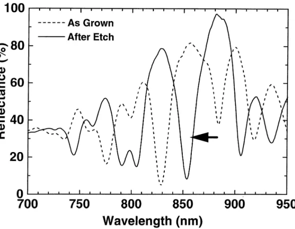
In Figure 4.2, reflection spectra of an ISU şamille, measured along with corresponding fitted simulation data, are presented. The discontinuities at about 870 nm in this and forthcoming simulations are due to the sharp discontinuity, of the data used for GaAs refractive index, at the bandgap edge. The positions of the measured minima and maxima cire consistent with simulations. In Figure 4.3, measured reflectivities of an ISU sample, which was used for fabrication of actual devices, are presented. This sample, which at first was not suitable for 840 nm opei’cition (dashed line), was tuned, by removing approximately 40 nm of cap layer in several etch steps, for operation wavelength (solid line) as mentioned above.
We also tuned another set of ISU samples with different absorption thicknesses. We named these samples as SI, S2, and S3 for brevity. These samples were prepared to study the affect of absorption layer thickiiess on RCE photodiode performance. Each of these scimples were carefully tuned for 850 nm resonance. Tuning of SI was the same as explained in the preceding paragra.ph. However, for S2 sample after observing first resonance reflection minima, we continued to etch till we tuned the sample to second resonance (again at 850 nm). Similarly, S3 is tuned to third resonance, at 850 nm wavelength. Absorption layer thicknesses of Sf, S2, and S3 were determined (from theoretical fits to corresponding reflection
Chapter 4. Measurements 39
700
750
800
850
900
Wavelength (nm)
950
Figure 4.2: Mecisured and simulated reflection spectra of the ISU sample.
spectra) as 290, f75, cuid 60 nrn respectively. These samples were also processed as defined in Chapter 3.
4.2
E ffects o f S ch o ttk y C on tact and S ilicon
N itr id e
We also carried out another set of experiments to understand the effects of, thin Schottky contact and nitride overlcty, on the reflection spectrum. These ex|3eriments were ca.rried out on ISU samples only, since we had only a small portion of the NIST wafer. We cleaved four pieces of the ISU wafer, and (lei)osited approximately 7, 1 2 , 17, 2 1 nm gold on each, and then 210 nm of nitride. Then this nitride layer is thinned in approximately 20 nm steps, until it