Defect
structures
in
a
layer-by-layer
photonic
band-gap
crystal
E.
OzbayDepartment
of
Physics, Bilkent University, Ankara 06533,TurkeyG.
Tuttle,M.
Sigalas,C. M.
Soukoulis, andK.
M.
HoMicroelectronics Research Center and Ames Laboratory, Iowa State Uniuersity, Ames, iowa 50011 (Received 26 September 1994;revised manuscript received 16 January 1995)
We have experimentally and theoretically investigated defect structures that are incorporated into a three-dimensional layer-by-layer photonic band-gap crystal. The defects are formed by either adding or removing dielectric material to or from the crystal. Forboth cases, we observed localized modes with
frequencies that lie within the forbidden band gap ofthe pure crystal. Relatively high peak transmission (10 dBbelow the incident signal), and high quality factors (2000)have been measured. These
measure-ments were in good agreement with theoretical simulations. Theoretical calculations also predict very
high (Q
)
10)quality factors for certain cavity structures.It
is now known that the propagationof
electromag-netic (EM) waves in periodic dielectric arrays can be completely forbidden fora certain range
of
frequencies.'
These three-dimensional arrays
—
photonic band-gap(PBG)crystals
—
offer the potential to engineer theprop-erties
of
the radiation field within these structures. ' Theinitial interest in this subject came from the proposal to
use
PBG
crystals to inhibit spontaneous emission inpho-tonic devices, leading to more efficient light emitters like thresholdless semiconductor lasers and single-mode light-emitting diodes. However, the difficulties
of
fab-ricating smaller scale structures restricted the experimen-tal demonstrationof
the earlyPBG
crystals to microwave frequencies (12—15 GHz). Recently, we designed a three-dimensional layer-by-layer structure, which allevi-ates someof
the fabrication difficulties inherent with the earlier designs. The layer-by-layer structure exhibits asizable and robust photonic band gap over a wide range
of
structural parameters. Using a large-scale model madeof
cylindrical alumina rods, we confirmed the ex-istenceof
a full photonic band gap at Eu-band frequen-cies (12—14GHz). Using semiconductor macromachin-ing techniques, we subsequently fabricated smaller scale structures with photonic band-gap frequencies ranging from 100to 500 GHz &0—&2 This performanceputs the new structure in the frequency range where anumber
of
millimeter and submillimeter wave applications have been proposed, including efficient millimeter wave anten-nas, filters, sources, and waveguides. ' ' However, mostof
these applications are based on the presenceof
defect or cavity modes, which are obtained by locally disturbing the periodicityof
the photonic crystal. ' ' The frequen-ciesof
these modes lie within the forbidden band gapof
the pure crystal, and the associated fields are localized around the defect. In this paper, we demonstrate the ex-istenceof
such cavity structures built around the layer-by-layerPBG
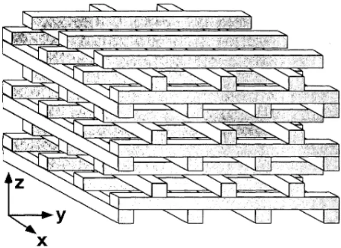
crystal.The structure, shown schematically in
Fig.
1, is con-structedof
layersof
dielectric rods. The stacking se-quence repeats every four layers, corresponding to asin-gle unit cell in the stacking direction. In this investigation
of
defect structures, we followed the approachof
Yablo-novitch et
al.
' wherein we either removed portionsof
the dielectric lattice or inserted extra dielectric materials into the air gaps. The basis for our studyof
defects was alarge-scale model
of
our photonic structure, constructedof
commercially available cylindrical alumina rods (re-fractive index=3.
1). The rods were0.
318+0.
013
cm in diameter and15.
24 cm long and were stacked withcenter-to-center separation
of 1.
123 cm, chosen to obtaina dielectric filling ratio
of
-0.
26.
This photonic crystal exhibits a full three-dimensional band gap between11.
7 and13.
5GHz.
We first investigated the properties
of
defect structures formed by removing a portionof
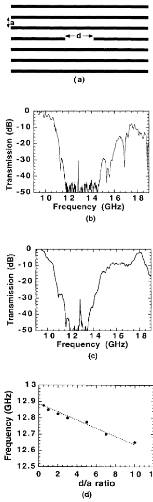
asingle rod, as illustrat-ed in Fig. 2(a). The lengthof
the missing section is d, and to facilitate possible comparison tosimilarPBG
crys-tals with different lattice constants, we define the defectX
FIG.
1. This figure schematically illustrates the design ofthethree-dimensional photonic band-gap crystal. The structure is
built by an orderly stacking ofdielectric rods and repeats every
four layers in the stacking direction.
volume ratio
d/a
where a is the center-to-center separa-tion between rodsof
thePBG
crystal. We measured the transmission and phase dispersion propertiesof
struc-tures with defects using a Hewlett-Packard 8510A net-work analyzer with standard gain horn antennas
to
transmit and receive theEM
radiation. The surround-ingsof
the test set up were covered with absorber materi-al to create an anechoic environment with a measurementasensitivity
of
approximately 70dB.
Figure 2(b) shows the transmission characteristics
of
propagation along the z axis (the stacking direction) for a structure with 4 unit cells(16
layers) along the z axis. The defect was placed at the eighth layerof
the structureand had a
d/a
ratioof 1.
The electric field polarizationvector
of
the incident EM wave ewas parallel to the rodsof
the defect layer. The lower edgeof
the band gap along this propagation direction starts at10.
7 GHz, while the upper edge isaround17.
4GHz.
The defect transmission was centered at 12.85 GHz, and the peak transmission was 30 dBbelow the incident signal. Using an expanded frequency scale, we measured the Qfactor (quality factor, defined as the center frequency divided by the peak's full width at half maximum)of
the peak to be greater than1000. We also measured the defect transmission at
different incidence angles by rotating the sample with
respect to the antennas while keeping e parallel to the rods
of
the defect layer. Figure 2(c) shows the transmis-sion propertiesof
the same defect structure when the sample was rotated35.
Although the upper and lower edgesof
the gap changed significantly due to different propagation directions, the defect frequency remained the same (12.85 GHz). We also measured cavity struc-tures with differentd/a
ratios. Figure 2(d) shows the dependenceof
the defect frequency on thed/a
ratio. Ascan be seen from the plot, the peak frequency changed less than
2%
as the defect volume changed by afactorof
10. We also found that the transmission via the defect was polarization dependent
—
no defect mode was present whenc
was perpendicular to the rodsof
the defect layer.We used the transfer-matrix method (TMM), recently introduced by Pendry and MacKinnon, to calculate the
EM transmission through a photonic crystal with defects.
In the TMM method, the total volume
of
the photonic crystal is divided in small cells and the fields in each cell are coupled with those in the neighboring cells. Then the transfer matrix can be defined by relating the incident fields on one sideof
thePBG
structure with the outgoing fields on the other side. Using TMM, the band structureof
an infinite periodic system can be calculated, but the main advantageof
this method is for the calculationof
transmission and refiection coeKcients for EM wavesof
various frequencies incident on a finite thickness slabof
thePBG
material. In that case, the material is assumedto be periodic in the directions parallel to the interfaces. The TMM method has previously been applied to defects in two-dimensional photonic band-gap structures, ' infinite
PBG
crystals in which the dielectric constants are complex and frequency dependent, and two-dimen-sional metallicPBG
structures. In all these examples, the agreement between theoretical predictions and exper-iment measurements was very good.o.
v ~~-10
~~-20
~~ 0) ~"--30
~-40
C5-50
4
II.t ()I'D10
12
14
16
18
Frequency (GHz) 0 I I 5 ) I I I / I ~ I / I I I ) I Kv
-10—
g -20-M N E -30-th g-40-50
.).
. . A,10
12
14
16
18
Frequency (GHz} (c) 13
s s s N 12.9—
~
12.
8 — ... V12.7—
e
12.
6-LL ~ ~ ~ I I I I0
2 ..~ e--4 6 8 ellaratio
I 012.
FIG.
2. (a) Missing material defect structure is obtained byremoving a part ofthe alumina rod. The removed part has a
width ofd, while the center-to-center separation between two
adjacent rods is a. (b) Transmission characteristics (along the stacking direction) obtained from a defect structure with ad/a ratio of 1. (c) Transmission characteristics ofthe same defect structure when it is rotated 35'. The defect frequency remains constant at different angles. (d) Defect mode frequency as a function of d/a ratio. The total change in defect frequency is
Since the TMM method requires periodicity in the directions parallel to the interfaces, we examined the case
of
a periodic defect, made by removing every other from a single layer [seeFig.
3(a)]. The experiments are done using a structure consistingof
4 unit cells (16 layers), where the eighth layer is chosen as the defect layer.Fig-ure 3(b) compares the predicted theoretical transmission with the experimental results. As can be seen from the
plot, the agreement between theory and experiment is especially good for the defect frequency. The measured
defect frequency is 12.62 GHz, while theory predicts 12.58
GHz.
Again, we observed no defect modes when eisperpendicular to the defect rods. This is in accordance
with theoretical results, which show that the peak transmission for the waves with eparallel to the removed rods is three orders
of
magnitude higher than the peak transmission obtained from the other polarization. Figure 3(c) shows the characteristicsof
the cavity mode on anexpanded frequency scale. Although the measured Q fac-tor (750)
of
the cavity mode is very close to the theoreti-cal Q factor (800), the measured peak transmissionof
—
17dB is far below the predicted valueof
—
4dB.
Thediscrepancy is probably due to the finite length
of
the rodsof
the test structure, while our theoreticalcalcula-tions assumed a crystal made
of
infinitely long rods. Cal-culations show that the defect frequency and Qfactor arenot very sensitive to separation between the defects. In particular, the defect frequency increases from 12.58 to 12.68 to 12.39 GHz as separation between the removed rods increases from 2a to 3a to
4a.
Also, the Q factor in-creases rapidly for increasing thicknessof
thePBG
crys-tal.
For
a structure with 8 unit cells (32 layers), wherethe defect-layer structure shown in Fig. 3(a) is chosen as the 16th layer, calculations predict a defect frequency at 12.61 GHz with a Q factor more than 1.
4X10
.
Thissuggests the possibility
of
building cavity structures withRemoved I'ods 0 cn
~
-10
0
&-20
-30
I
-40
g
-50
-60
I g ~ i i i i ~L I I I i I10
12
14
16
18
Frequency
(GHz} I5 I ~ I I / I I f I / I I I I J I I I I Kl 'V -20 ~0
NN -25 ~~ E -30 C I--35 ~ I I I I I I I I I ~ I \ I I I ~ I I12.
5712.
6 12.6212.
65 12.67 Frequency (GHz) (c)-10
o
-20 ~~ N N30
E Nc
-40 CO-50
'tJ
10
12
14
Frequency (c)16
18
(6Hz)FICz. 3. (a) Every other rod ofa single layer is removed to generate the defect layer. (b) Comparison of the theoretical (dashed line) and experimental {solidline) transmission charac-teristics ofthe defect structure. (c) Expanded frequency scale for the defect mode, which has aQfactor of2500.
FIC)r. 4. (a) The defect structure obtained by a single rod.
This defect structure did not yield any measurable defect mode.
(b) The defect layer obtained by two rods ofequal length. (c) Transmission characteristics ofthe defect structure depicted in
very high Qfactors from this geometry.
We also investigated defects that are obtained by add-ing pieces
of
rods or whole rods into the empty spaceof
thePBG
crystal. Figure 4(a)depicts the defect layer built by adding a single pieceof
dielectric material between two rods. Although we tried a numberof
differentcom-binations (di6'erent defect lengths, dift'erent number
of
units cells), we did not observe any defect-mode transmis-sion along the stacking direction. This could be due tolimited coupling
of
the defect mode to the incident signal, which may result in a defect mode that is well below the attenuation within the photonic band-gap region. We were more successful when we added two pieces to createthe defect, as shown in Fig. 4(b). Figure 4(c) shows the transmission characteristics for propagation in the z direction (stacking direction) for a structure with 3 unit cells (12 layers) along the z axis. The defects were added in the fifth layer
of
the structure and both rods had a d/a
ratio
of 2.
The defect transmission was at 12.6GHz witha peak transmission
of
15 dB below the incident signal and Q factorof
—
1000. We again found that the defect frequency remained constant at different propagationdirections.
It
should be noted that the transmission fre-quency measured for the additive defect islower than the frequencyof
the subtractive defect. Yablonovitch etal.
found an opposite trend for the defects in their crystalstructure. ' This discrepancy is due to the different defect
structures we have used in this paper. In our experi-ments, the defect structures are obtained by removing or
adding cylindrical rods
of
the same radius but different length. When we extend our calculations for defects ob-tained by changing the radiusof
the cylinders, we find a similar trend obtained byRef.
17.
For
these defects, transmission frequency measured for the additive defect is higher than the frequencyof
the subtractive defect.Yablonovitch et
al.
have named such defects asacceptors (missing material) or donors (added material) in analogyto
the different doping typesof
the semiconductors. ' We have found that this trend was not valid for certain defectstructures, and we tried to avoid such a nomenclature, which may be confusing to readers.
Finally, we used TMM to study aperiodic additive
de-fect. Figure 5(a) depicts the periodic defect layer, in which an extra dielectric rod was inserted halfway be-tween each lattice rod in one layer
of
t'hePBG
crystal.This defect layer was the fifth layer
of
a structure thatconsisted
of
3unit cells (12layers total). Theoretical and experimental spectra for transmission in the z direction are compared inFig.
5(b). The experimental (12.4 GHz)and theoretical (12.5 GHz) defect frequencies are in good agreement along with experimental and theoretical peak
v///////j////////////j/jj//////////////////////////////ji Ji a v////uaua//////////uu////////ua////////////////x ~additional r////////////////u/uuu/////////u///////////////////A-I'ods 0
K
~
-10
.
'o-20
CO 40 'E-30
V) +~-40
-50
~ I I ~~ ~~ I ' ' ' I a,~a I~ I~~Il I~~ I ~I1 ~ ~%~ I I Q ~ ~ I ~~I ~~I I~I ~I~ ~~ ~ ~ Il ~ ~transmissions, which are both
—
10dBlower than the in-cident signal. However, theory predicts large Q values(
)
10000)
while the measured Q values are approximate-ly 2000. Again, the difference islikely due to the infinite sizeof
the experimentalPBG
structure.In summary, we have investigated defect structures built around a rod-based photonic band-gap crystal. We
have observed localized defect modes with high peak transmission and high Q values. The measurements are in good agreement with our theoretical simulations. The
availability
of
such defect structures will be a key tool forthe proposed applications
of PBG
materials.The authors would like to thank
R.
Biswas andC.
T.
Chan for helpful discussion and comments, andD.
Turner for his help in making the TMM code run on the nCube parallel processor. Ames Laboratory is operatedfor the
U.S.
Departmentof
Energy by Iowa State Univer-sity under Contract No. W-7405-Eng-82. This work was supported by the Director for Energy Research,Once of
Basic Energy Sciences and Advanced Energy Projects,
the Center for Advanced Technology Development at ISU, and the Scalable Computing Laboratory, which is funded by ISUand Ames Laboratory.
10
12
14
16
18
Frequency
(GHz) (b)FIG.
5. (a)The defect layer is built by additional rods that are placed at the midpoints ofadjacent rods. (b)Comparison of the theoretical (dashed line) and experimental (solid line)transmission characteristics ofthe defect structure.
E.
Yablonovitch,T.
J.
Gmitter, andK.
M. Leung, Phys. Rev. Lett. 67,2295(1991).2K. M. Ho, C.
T.
Chan, and C.M.Soukoulis, Phys. Rev. Lett. 65, 3152 (1990).For arecent review, see the articles in Photonic Band Gags and
Loca/ization, edited by C.M.Soukoulis (Plenum, New York,
1993}~
4S. John and N.Akozbek, Phys. Rev. Lett. 71, 1168 (1993). ~D.L. Bullock, C. C. Shih, and
R.
S.Margulies,J.
Opt. Soc.Am.
8
10, 399 (1993}.6P.L.Gourley,
J.
R.
Wendt, G.A.Vawter,T.
M.Brennan, and7J.P.Dowling, M. Scalora, M.
J.
Bleomer, and C.M.Bowden,J.
Appl. Phys. 75, 1896 (1994).8K. M. Ho, C.T.Chan, C.M.Soukoulis, R.Biswas, and M. Si-galas, Solid State Commun. 89, 413 {1994).
E.
Ozbay, A. Abeyta, Cx. Tuttle, M. Tringides, R.Biswas, C. Soukoulis, C.T.
Chan, andK.
M. Ho, Phys. Rev.8
50, 1945 (1994).~oE.Ozbay,
E.
Michel, G.Tuttle, M. Sigalas,R.
Biswas, andK.
M.Ho, Appl. Phys. Lett. 64, 2059(1994}.
E.
Ozbay,E.
Michel, G.Tuttle,R.
Biswas,K.
M. Ho,J.
Bos-tak, and D.M.Bloom, Opt. Lett. 19, 1155 (1994).' E.Ozbay, Cr.Tuttle, M.Sigalas,
R.
Biswas,K.
M.Ho,J.
Bos-tak, and D.M.Bloom, Appl. Phys. Lett. 65, 1617 (1994). I3See the articles inJ.
Opt. Soc. Am.8
10 (1993),a specialfeature edited by C.M. Bowden,
J.
P. Dowling, and H. O. Everitt.~4E.
R.
Brown, C.D.
Parker, andE.
Yablonovitch,J.
Opt. Soc. Am.8
10,404(1993}.~~E.
R.
Brown, C.D.Parker, and O.B.
McMahon, Appl. Phys. Lett.64, 3345(1994).C.
J.
Maggiore, A. M.Clogston, G.Spalek, %'.C.Sailor, andF.
M.Mueller, Appl. Phys. Lett.64, 1451(1994).~7E. Yablonovitch,
T.
J.
Gmitter,R.
D.Meade, A. M. Rappe,K.
D. Brommer, andJ.
D.Joannopoulos, Phys. Rev. Lett. 67, 3380(1991).I8S.L.McCall, P.M.Platzman,
R.
Dalichaouch, D.Smith, and S. Schultz, Phys. Rev.Lett. 67, 2017(1991).K.
M.Leung,J.
Opt. Soc.Am.8
10,303(1993).~oJ.
B.
Pendry and A. MacKinnon, Phys. Rev. Lett. 69, 2772(1992);
J.
B.
Pendry,J.
Mod. Opt. 41,209(1994).'M.M.Sigalas, C. M.Soukoulis,
E.
N.Economou, C.T.
Chan,and
K.
M. Ho,Phys. Rev.8
48, 14 121(1993).2~M. M. Sigalas, C. M. Soukoulis, C.
T.
Chan, andK.
M.Ho,.
Phys. Rev.8
49,11080{1994).D.R.Smith, S.Shultz, N. Kroll, M. Sigalas,