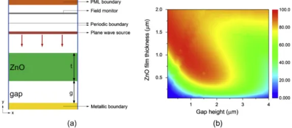
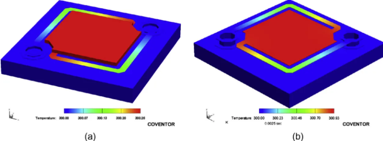
An all-ZnO microbolometer for infrared imaging
Tam metin
Şekil

Benzer Belgeler
The presence of IDH1 mutation (Fig. 2 a) was associated with an elevated concentration for glucose, myo-inositol, GPC, histidine, creatine and 2HG and a low concentration
clustering the complete wireless network depending on the density using the DBSCAN approach and estimating the un-localized nodes within each cluster using PSO based
Sayısal hesaplarda, Monte Carlo yöntemi uygulanarak elastisite modülünün uzunluk bileşenine rastgele değerler verilerek doğal titreşim frekansı için bulunan her üç ifadede
Diğer yandan, orta destek, çatı ya da çadırın örtüsünde bırakılan delikle ilişkilendirilen, kuzeybatı yönünde bulunduğuna inanılan, Gök Kapısı tema- lı inanışlar,
In this thesis, we compare and contrast the competitivity of projection meth ods, block iterative methods, and point SOR in computing the stationary prob ability
Recently, a DFT-based acceleration algorithm [13] was used in conjunction with stationary (for example, the forward-backward method (FBM)) and nonstationary (for example,
Yolpalas Cinayeti, Sonsuz Panayır ve Âkile Hanım Sokağı’nın incelenceği, “Halide Edib Adıvar’ın Romanlarında Kültür Simgeleri” adlı ikinci bölümde, bu
meslek sahibi kişilerin ilk satışları için kullanılan ‘sif- tah’ kelimesini, Arapça ‘istiftâh’ kelimesinden bozma olarak kullanırlar. Arapçada kişinin karnında
