ATOMIC LAYER DEPOSITION OF
III-NITRIDES AND METAL OXIDES; THEIR
APPLICATION IN AREA SELECTIVE ALD
A DISSERTATION SUBMITTED TO
THE GRADUATE SCHOOL OF ENGINEERING AND SCIENCE OF BILKENT UNIVERSITY
IN PARTIAL FULFILLMENT OF THE REQUIREMENTS FOR THE DEGREE OF
DOCTOR OF PHILOSOPHY IN
MATERIALS SCIENCE AND NANOTECHNOLOGY
By Ali Haider July, 2017
i
ATOMIC LAYER DEPOSITION OF III-NITRIDES AND METAL OXIDES; THEIR APPLICATION IN AREA SELECTIVE ALD
By Ali Haider July 2017
We certify that we have read this dissertation and that in our opinion it is fully adequate, in scope and in quality, as a thesis for the degree of Doctor of Philosophy.
Aykutlu Dana (Advisor)
Necmi Bıyıklı (Co-Advisor)
Oğuz Gülseren Ferdi Karadaş Gökhan Demirel Adil Denizli
Approved for the Graduate School of Engineering and Science:
Ezhan Karaşan
ii ABSTRACT
ATOMIC LAYER DEPOSITION OF III-NITRIDES AND METAL OXIDES; THEIR APPLICATION IN AREA SELECTIVE ALD
ALI HAIDER
PhD in Materials Science and Nanotechnology Supervisor: Aykutlu Dana
Co-supervisor: Necmi Biyikli July 2017
III-nitride compound semiconductor materials (GaN, AlN, and InN) and their alloys have generated significant interest in both basic research and commercial applications mainly in the field of photonics, energy storage, nano-sensors, and nano-(opto)electronics. Wurtzite type III-nitrides exhibit direct band gaps, which extend from the ultra-violet (UV) to the mid-IR spectrum with values of 6.2, 3.4 and 0.64 eV for AlN, GaN, and InN, respectively. This feature allows the band gap of III-nitride alloys to be conveniently tuned by precisely controlling the composition for a particular application. Metalorganic chemical vapor deposition (MOCVD) and molecular beam epitaxy (MBE) are the most common successful techniques for achieving high-quality epitaxial III-nitride layers with low impurity concentrations and decent electrical properties. However, both of these methods employ high growth temperatures, which is neither compatible with the existing CMOS technology nor suitable for temperature-sensitive device layers (e.g. In-rich InxGa1-xN) and substrates (e.g. glass, flexible polymers, etc.). These limitations are the main driving source for a continuous exploration of alternative low temperature processes for the growth of III-nitride layers and their alloys. High aspect ratio III-nitride nanostructures in the form of nanowires and nanorods have been synthesized using different techniques including vapor-liquid-solid crystal growth, electrospinning, template based synthesis, and etching. Critical breakthroughs in fabrication of III-nitrides nanostructures have been achieved by above mentioned techniques but suffer from limited control over properties of nanostructures (shape, orientation, and size) and in some cases high growth-temperature requirement. A recent flurry of interest in developing high quality I-D III-nitride nanostructures derives from
iii
the desire to obtain flexible optoelectronic devices having wider applications. Template-assisted growth technique is one of the most promising approach to fabricate III-nitride nanostructures with precise control over shape, size, position, and distribution.
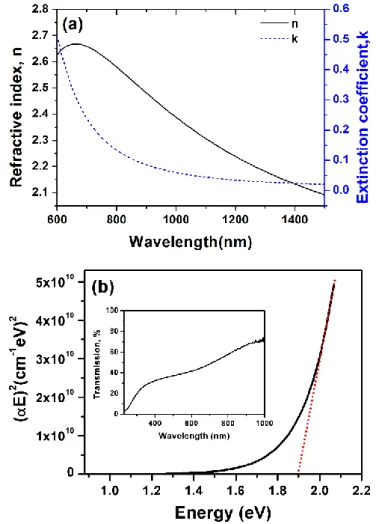
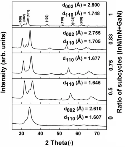
In the first part of thesis, we have deposited InN and III-nitride alloys using hollow-cathode plasma assisted atomic layer deposition (HCPA-ALD) at low growth temperatures. The aim was to deposit III-nitride materials at lowest growth temperatures with decent crystalline quality and minimum impurity content. Depositions were carried out using group III organometallic precursors along with N2/H2 or N2 plasma as metal and nitrogen source, respectively. Process parameters including precursorpulse time, plasma flow duration, purge time, and deposition temperature are investigated and correlations were developed between process parameters and material properties. Refractive index of the InN film deposited at 200 C was found to be 2.66 at 650 nm. 48 nm-thick InN films exhibited relatively smooth surfaces with RMS surface roughness values of 0.98 nm, while the film density was extracted as 6.30 g/cm3. The effect of In content on structural, optical, and morphological properties of InxGa1-xN thin films was investigated. Grazing incidence X-ray diffraction (GIXRD) and transmission electron microscope (TEM) showed that InN and InxGa1-xN thin films were polycrystalline with hexagonal wurtzite structure. Spectral absorption measurements exhibited an optical band edge of InN around 1.9 eV. X-ray photoelectron spectroscopy (XPS) confirmed the deposition of InN and alloy thin films and revealed the presence of low impurity contents. Higher In concentrations resulted in an increase of refractive indices of InxGa1-xN ternary alloys from 2.28 to 2.42 at a wavelength of 650 nm. Optical band edge of InxGa1-xN films red-shifted with increasing In content, confirming the tunability of the band edge with alloy composition. Photoluminescence measurements of InxGa1-xN exhibited broad spectral features with an In concentration dependent wavelength shift. We have also studied the compositional dependence of structural, optical, and morphological properties of BxGa1-xN and BxIn1-xN ternary thin film alloys grown using sequential pulsed CVD. GIXRD measurements showed that boron incorporation in wurtzite lattice of GaN and InN diminishes the crystallinity of BxGa1-xN and BxIn1-xN sample. Refractive index decreased from 2.24 to 1.65 as the B concentration of BxGa1-xN increased from 35 to 88 %. Similarly, refractive index of BxIn1-xN changed from 1.98 to 1.74 for increase in B concentration value from 32 to 87 %, respectively. Optical
iv
transmission band edge values of the BxGa1-xN and BxIn1-xN films shifted to lower wavelengths with increasing boron content, indicating the tunability of energy band gap with alloy composition. Atomic force microscopy measurements revealed an increase in surface roughness with boron concentration of BxGa1-xN, while an opposite trend was observed for BxIn1-xN thin films.
Moreover, we demonstrate vertical GaN, AlN, and InN hollow nano-cylindrical arrays (HNCs) integrated to Si(100) substrates using anodized aluminum oxide (AAO) membrane templated PA-ALD. Our fabrication and Si-integration strategy consists of the following process steps: (i) reactive ion etching (RIE) of Si using AAO membrane as hard mask material to achieve nanoporous Si substrate, (ii) conformal growth of III-nitride films on nanoporous Si via low-temperature PA-ALD, (iii) removal of PA-ALD coated III-nitride material from top surface of Si via plasma etching, and (iv) isotropic dry etching of surrounding Si to attain long-range ordered vertical III-nitride HNCs. The material properties of nanostructured III-nitride materials have been compared with the thin-film counterparts which were also grown using low-temperature PA-ALD. SEM images revealed that long-range ordered arrays of III nitride HNCs were successfully integrated in Si(100) substrates. TEM, GIXRD, and selected area electron diffraction (SAED) cumulatively confirmed that III-nitride HNCs possess hexagonal wurtzite crystalline structure. XPS survey and high-resolution scans detected presence of different elements and peaks at specific binding energies which confirmed the formation of III-nitride HNCs.
The second part of the thesis deals with self-aligned thin film patterning of metal oxides using area selective atomic layer deposition (AS-ALD). Nanoscale process integration demands novel nano-patterning techniques in compliance with the requirements of next generation devices. Conventionally, top-down subtractive (etch) or additive (deposition/lift-off) processes in conjunction with various lithography techniques is employed to achieve film patterning, which become increasingly challenging due to the ever-shrinking misalignment requirements. To reduce the complexity burden of lithographic alignment in critical fabrication steps, self-aligned processes such as selective deposition and selective etching might provide attractive solutions.
We demonstrate a methodology to achieve AS-ALD by using inductively couple plasma (ICP) grown fluorocarbon polymer film as growth inhibition
v
layer. The fluorocarbon layer was grown using C4F8 feed gas in a conventional ICP-etch reactor. Our approach has been tested for metal-oxides including ZnO, Al2O3, TiO2, and HfO2. Additionally, we investigate the poly(methyl methacrylate) (PMMA) and polyvinylpyrrolidone (PVP) as growth inhibition layers for AS-ALD of TiO2. Contact angle, XPS, spectroscopic ellipsometer, energy dispersive X-ray spectroscopy (EDX), and scanning electron microscopy (SEM) measurements were performed to investigate the blocking ability of polymer layers against ALD-grown films. Characterizations carried out revealed that effective blocking on fluorocarbon layer is achieved for ZnO film upto 136 growth cycles. On the other hand, a rather slow nucleation has been observed for HfO2 growth on fluorocarbon coated surfaces, while TiO2 and Al2O3 growth showed almost no delay with a growth rate equal to the ones on conventional substrate surfaces. For TiO2, PMMA revealed successful growth inhibition upto the maximum inspected growth cycles while PVP was able to block TiO2 growth upto 300 growth cycles. By exploiting this inhibition feature, thin film patterning has been demonstrated by growing ZnO films on photo lithographically patterned fluorocarbon/Si samples. We also demonstrate nanoscale patterned deposition of TiO2 using a PMMA masking layer that has been patterned using e-beam lithography.
Keywords: Plasma-Enhanced Atomic Layer Deposition, III-Nitrides,
Area-Selective Atomic Layer Deposition, Metal Oxides, Thin Films, Nano-Cylinders, Thin-Film Patterning
vi ÖZET
III-NİTRATLARIN VE METAL OKSİTLERİN ATOMİK KATMAN KAPLAMISI; BUNLARIN ALAN SEÇİCİ ALD`DEKI
UYGULAMALARI
Ali Haider
Malzeme Bilimi ve Nanoteknoloji, Doktora Tez Danışmanı: Aykutlu Dana
Temmuz 2017
Yarı iletken III-nitrit bileşikleri (GaN, AlN, and InN) ve onların alaşımları, hem temel araştırma alanlarında hem de ticari uygulamalarda, özellikle fotonik, enerji depolaması, nano-sensörler ve nano-(opto) elektronikler alanlarında önemli ilgi uyandırmıştır. Würtzit tipi III-nitritları, sırasıyla AlN, GaN ve InN için 6,2, 3,4 ve 0,64 eV değerleri ile morötesi (UV) ile orta-IR spektruma uzanan doğrudan bant aralıklarına sahiptir. Bu özellik, belirli uygulamalar için III-nitrit alaşımlarının band aralığını tam bileşim kontrolü ile kolaylıkla ayarlamaya izin veriyor. Metalorganik kimyasal buhar birikimi (MOCVD) ve Moleküler kiriş epitaksisi (MBE), düşük safsızlık konsantrasyonlu ve iyi elektriksel özelliğe sahip yüksek kaliteli epitaksiyel III-nitrit tabakalarını elde etmenin en yaygın ve başarılı yöntemleridir. Fakat bununla birlikte, bu yöntemlerin her ikisi de, mevcut CMOS teknolojisi ile uyumlu olmayan ya da sıcaklığa duyarlı aygıt katmanlarına (örneğin In-zengin InxGa1-xN) ve alt tabakalara (örneğin cam, esnek polimerler, vb.) uygun olmayan yüksek büyüme sıcaklıkları kullanmaktadı. Bu kısıtlamalar, III-nitrit ve alaşımlarının tabakalarını büyütmenin alternatif düşük sıcaklıktaki proseslerin araştırmalarının ana itici kaynağıdır. Nanotel ve nanoçubuk şeklindeki yüksek en-boy oranlı III-nitrit nanoyapıları buhar-sıvı-katı kristal büyütmesi, elektrospinning, şablon esaslı sentez ve aşındırma yöntemlerini kapsayan yöntemlerle sentezlenmiştir. III-nitrit nanoyapıların üretiminde kritik gelişmeler yukarıda adı geçen yöntemlerle elde edilmiştir ancak nanoyapılardaki (şekil, yönelim ve boyut)
vii
özelliklerde kısıtlı kontrol ve bazı yüksek sıcaklık gereksinimlerinden muzdarip. Yüksek kalitede I-D III-nitrit nanoyapıların geliştirilmesine yönelik yeni bir ilgi, daha geniş uygulamalara sahip esnek optoelektronik aygıtlar elde etme isteğinden kaynaklanmaktadır. Şablon destekli büyütme tekniği, III- nitrit nanoyapılarının şekli, boyutu, konumu ve dağılımı üzerinde hassas kontrolü olan en umut verici üretim yöntemlerinden bir tanesidir.
Tezin ilk bölümünde, düşük büyüme sıcaklıklarında içi boş katot plazma yardımlı atomik katman çökeltme (HCPA-ALD) kullanarak InN ve III-nitrür alaşımları tevdi ettik. Amaç, III-nitrür materyallerin, uygun kristal kalitesi ve minimum safsızlık içeriği ile en düşük büyüme sıcaklıklarında depolanmasıydı. Depozisyonlar N2/H2 ve N2 plazması ile birlikte grup III organometalik öncülleri kullanılarak gerçekleştirildi. Prekürsör darbe süresi, plazma akış süresi, boşaltma süresi ve çökelme sıcaklığı gibi proses parametreleri araştırılmış ve proses parametreleri ile malzeme özellikleri arasında korelasyonlar geliştirilmiştir. 200 °C'de biriken InN filminin refraktif indeksi 650 nm'de 2.66 bulundu. 48 nm kalınlığında InN filmleri 0.98 nm RMS yüzey pürüzlülüğü değerlerine sahip nispeten pürüzsüz yüzeyler sergilerken film yoğunluğu 6.30 g / cm3 olarak çıkarıldı. In içeriğinin yapısal, optik ve In
xGa1-xN ince filmlerin morfolojik özelliklerine etkisi araştırıldı. Grazing insidansı X-ışını kırınımı (GIXRD) ve transmisyon elektron mikroskobu (TEM). InN ve InxGa1-xN ince filmlerin altıgen würzit yapıya sahip polikristalin olduğunu gösterdi. Spektral absorpsiyon ölçümleri, 1.9 eV civarında InN'nin bir optik bant kenarını sergiledi. X-ışını fotoelektron spektroskopisi (XPS) InN ve alaşım ince filmlerin birikimini doğruladı ve düşük safsızlık içeriğinin varlığını ortaya koydu. Dahası, anodize edilmiş aliminyum oksit (AAO) membran kalıplı PA-ALD kullanarak Si(100) alttaş üzerine dikey GaN, AlN ve InN oyuk nano-silindir dizisinin etegrasyonu gösterildi. Bizim fabrikasonumuz ve Si-etegrasyonu takip eden işlemleri içerir: (i) Nano-pürüzlü Si alttaşa sahip olmak için, AAO membranı sert maske malzemesi olarak kullanarak Si rekatif iyon oyma (RIE), (ii) düşük sıcaklıklı PA-ALD ile nano-pürüzlü Si üzerinde III-Nitrat filmlerin konformal olarak büyütülmesi, (iii) PA-ALD kaplamalı III-nitrat malzemelerin Silikon yüzeyinden plazma oyma kullanarak kaldırılması, ve (iv) uzun mesafeli dizili dikey III-nitrat HNC’lere sahip olmak için Silikonun çevresinin izotropik kuru oyulması. Nano-işlenmiş III-Nitrat malzemelerin malzeme özellikleri, benzer şekilde düşük sıcaklıklı PA-ALD’de büyütülmüş ince film emsalleri ile karşılaştırıldı. SEM resimleri, uzun sıralı dizilmiş III-Nitrat HNC dizisi başarılı
viii
bir şekilde Si(100) alttaşa entegre edildiğini ortaya koymuştur. TEM, GIXRD ve seçili alan electron difraksiyon (SAED) sonuçları III-Nitrat HNC’lerin hegzagonal wurtzite kristal yapıya sahip olduğunu kümülatif olarak gösterdi. XPS analizi ve yüksek çözünürlüklü taramalar III-Nitrat HNC’lerin farmasyonunun doğrulayan spesifik bağlanma enerjilerinde farklı elementler tespit etti.
Tezin ikinci bölümü,alan seçmeli atomik katman birikimini kullanarak metal oksitlerin ince filmde kendi dizilişine değinmektedir(AS-ALD).Nanoölçüm süreç entegrasyonu yeni nesil cihazların gereksinimlerine uygun olarak nanodiziliş tekniklerini talep eder.Genellikle, çeşitli litografi teknikleri ile birlikte yukarıdan aşağıya eksiltici(etch) ya da katkı maddesi(biriktirme/kaldırma) prosesleri filmin desenleme işlemini elde etmek için kullanılır,bu, sürekli küçülen yanlış hizalama gereksinimleri nedeniyle gittikçe zorlaşır.Kritik üretim aşamalarında litografik hizalamanın karmaşıklık yükünü azaltmak için, seçici biriktirme ve seçici aşındırma gibi kendi kendine hizalı işlemler cazip çözümler sağlayabilir.
Artımlı inhibisyon tabakası olarak indükte çift plazma (ICP) yetiştirilmiş florokarbon polimer filmi kullanarak AS-ALD'yi gerçekleştirmek için bir metodoloji gösteriyoruz.Florokarbon tabakası, alışılmış bir ICP-etch reaktöründe C4F8 besleme gazı kullanılarak büyütüldü. Yaklaşımımız ZnO, Al2O3, TiO2 ve HfO2 gibi metal oksitler için test edilmiştir. Ayrıca, TiO2'nin AS-ALD için büyüme önleyici tabakalar olarak poli (metil metakrilat) (PMMA) ve polivinilpirolidonu (PVP) araştırdık.ALD ile üretilen filmlere karşı polimer katmanlarının bloke edici özelliklerini araştırmak için temas açısı, XPS, spektroskopik elipsometre, enerji dağılımlı X-ışını spektroskopisi (EDX) ve taramalı elektron mikroskobu (SEM) ölçümleri yapıldı. Yapılan karakterizasyonlar, ZnO filmi 136 büyüme çevrimine kadar florokarbon tabakasında etkili bir blokajın gerçekleştirildiğini ortaya koydu.Diğer yandan,TiO2 ve Al2O3 büyümesi, geleneksel substrat yüzeylerindeki büyüme hızına eşit bir büyüme oranı ile neredeyse hiç gecikme göstermezken,florokarbon kaplı yüzeylerde HfO2 büyümesinde oldukça yavaş bir çekirdeklenme gözlemlendi. TiO2 için, PMMA maksimum incelenen büyüme döngüsüne kadar başarılı büyüme inhibisyonu ortaya koyarken, PVP ,TiO2 büyümesini 300 büyüme döngüsüne kadar bloke edebildi. Bu inhibisyon özelliğinden yararlanılarak ince film şekillenmesi, foto litografik olarak desenli florokarbon/Si numuneleri üzerinde ZnO filmlerinin büyütülmesi ile
ix
gösterildi.e-ışınlı litografi kullanılarak desenlendirilmiş bir PMMA maskeleme katmanı kullanarak TiO2'nin nano ölçekli desenli birikimini ayrıca kanıtlamış olduk.
Anahtar kelimeler: Plazma Arttırılmış Atomik Katmanlı Depozit, III-Nitrürler,
Alan Seçici Atomik Katmanlı Kalınım, Metal Oksitler, İnce Filmler, Nano-Silindirler, İnce Film Desenlendirme
x
Acknowledgement
I would like to express my sincere gratitude to my advisors, Dr. Necmi Biyikli and Dr. Aykutlu Dana for their valuable guidance and endless support during my PhD research. I want to express my gratitude to Cagla Ozgit-Akgun, Sevde Altuntas, Petro Deminskyi, and Seda Kizir for their continued support and help in my research work.
I would like to express my deepest appreciation to my lovely parents and siblings for their love and care throughout my PhD studies. They were always very kind and supportive through highs and lows during my doctorate. They encouraged me to strive for the best research work and gave me the belief to always remain positive throughout the course of my PhD.
I would like to say a very special thanks to all my friends at Bilkent University and in Turkey who made my life really wonderful in past few years. Especially, I want to mention Jamoliddin Khanifaev, Talha Masood Khan, Naveed Mehmood, Berrera Maqbool, Murat Serhatlioglu, Haydarali Sayfiddinov, Hamit Eren, Ziya Işıksaçan, Begimai Adilbekova, Naveed ul Mustafa, Umar Raza, and Ali Kalantarifard for their support, kind advices, and amazing times spend together.
Finally, I would also like to say thanks to all engineers especially Semih Yasar, Mustafa Guler, and Enver Kahveci who contributed to my research experience and always helped me in enhancing my learning towards research equipment’s.
xi
xii
Contents
ABSTRACT ... ii ÖZET ... vi Acknowledgement ... x Contents ... xii List of Figures ... xvList of Tables ... xxii
Chapter 1 ... 1
Introduction ... 1
1.1 Historical Background of the Technique Used ... 1
1.2 Motivation ... 3
1.2.1 InN and III-Nitride Alloy Thin Films Deposition Using HCPA-ALD 3 1.2.2 Template Assisted Fabrication of III-nitride Hollow Nanocylinders via HCPA-ALD ... 4
1.2.3 Area Selective Atomic Layer Deposition of Metal Oxides Using Polymer Growth Inhibition Layers ... 6
1.3 Objectives ... 8
1.4 Thesis Overview ... 11
Chapter 2 ... 12
Theoretical Background and Literature Overview ... 12
2.1 An Overview on Atomic Layer Deposition ... 12
2.1.1 Mechanism ... 13
2.1.2 Factors Causing Saturation and Growth of Less than Monolayer per Cycle ... 14
2.1.3 ALD Window ... 14
2.1.4 Merits and Demerits of ALD and Comparison with Other Deposition Techniques ... 16
2.1.5 Plasma vs. Thermal ALD ... 17
2.2 InN and III-Nitride Alloy Thin Film Deposition Using HCPA-ALD reactor ... 17
xiii
2.3 Template Assisted Fabrication of III-Nitride Nanocylinders ... 19
2.4 Area-Selective ALD of Metal Oxides Using Polymer Growth Inhibition Layers ... 21
Chapter 3 ... 23
Experimental Details ... 23
3.1 Hollow Cathode Plasma Assisted Atomic Layer Deposition of InN ... 23
3.2 Hollow Cathode Plasma Assisted Atomic Layer Deposition of InxGa1-xN Thin Films ... 25
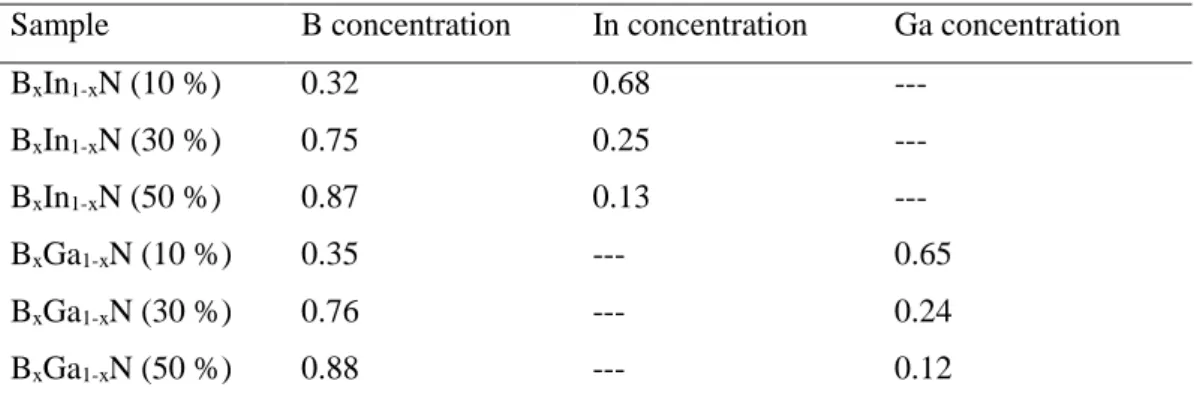
3.3 Sequential Pulsed Chemical Vapor Deposition of Ternary BxGa1-xN and BxIn1-xN Thin Film Alloys ... 26
3.4 Template Assisted Fabrication of III-Nitride Nano-Cylinder Arrays via Plasma-Assisted Atomic Layer Deposition ... 27
3.4.1 AAO Foils Preparation ... 27
3.4.2 Vertical III-nitride Hollow Nano-cylinder Array Fabrication ... 28
3.5 Area Selective Atomic Layer Deposition of Metal Oxides Using Polymer Growth Inhibition Layers ... 30
3.6 Characterization Methods ... 31
Chapter 4 ... 34
InN and III-Nitride Alloy Thin Films Deposition Using HCPA-ALD ... 34
4.1 Hollow Cathode Plasma Assisted Atomic Layer Deposition of InN Thin Films ... 34
4.1.1 Optimization of Growth Parameters ... 35
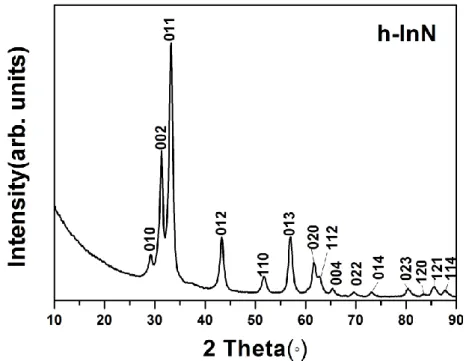
4.1.2 Material Characterization of InN Thin Films ... 39
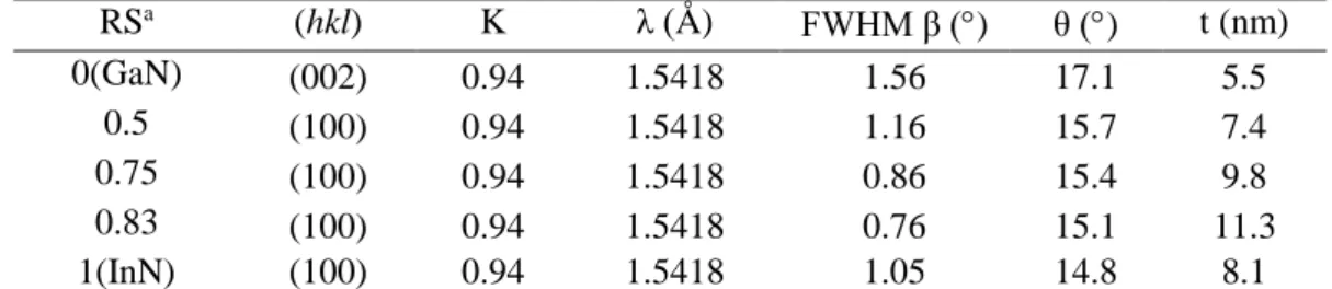
4.2 Hollow Cathode Plasma Assisted Atomic Layer Deposition of InxGa1-xN Thin Films ... 51
4.3 Low-temperature Sequential Pulsed Chemical Vapor Deposition of Ternary BxGa1-xN and BxIn1-xN Thin Film Alloys ... 68
Chapter 5 ... 77
Template Assisted Atomic Layer Deposition of III-nitride Nanostructures77 5.1 GaN Hollow Nanocylinder Arrays ... 79
5.2 AlN Hollow Nanocylinder Arrays ... 88
xiv
Chapter 6 ... 106
Area Selective Atomic Layer Deposition of Metal Oxides Using Polymer Growth Inhibition Layers ... 106
6.1 AS-ALD of ZnO, HfO2, and Al2O3 Using Plasma Polymerized Fluorocarbon Growth Inhibition Layer ... 106
6.2 Nanoscale Selective Area Atomic Layer Deposition of TiO2 Using E-beam Patterned Polymers ... 124
Chapter 7 ... 141
Conclusion and Future Prospects ... 141
xv
List of Figures
Figure 2.1: Schematic representation of an ALD cycle consisting of four steps. ... 14 Figure 2.2: Effect of deposition temperature on the ALD growth rate. ... 15 Figure 3.1: Details regarding specific parts and their features of ALD system . 24 Figure 3.2: A schematic showing growth process sequence of InxGa1-xN thin film with single sub cycle of InN and GaN ... 26 Figure 3.3: The schematic showing step-by-step fabrication of vertically aligned III-nitride HNCs: (a) AAO membrane placement on Si(100), (b and c) Si patterning with Ar/CHF3 based reactive ion etching (RIE) using AAO membrane as hard mask material to achieve nanoporous Si substrate, (d) conformal coating of III-nitride materials, (e) Ar based RIE of PA-ALD coated III-nitride material from top surface of Si, (f) SF6 based selective etching of Si to obatain III-nitride HNCs. ... 29 Figure 4.1: Effect of precursor doses on growth rate at 200 °C: TMI pulse length was kept constant at 0.7 s for the N2 plasma saturation curve, N2 plasma dose was kept constant at 100 s for the TMI saturation curve. (Inset) N2 plasma dose vs. carbon at. % present in the bulk of the film. ... 36 Figure 4.2: InN film thickness vs. number of deposition cycles. (Inset) Deposition rate as a function of purge time: TMI dose and N2 plasma exposure time were constant at 0.7 and 100 s, respectively. ... 37 Figure 4.3: Growth rate and In/N ratio (evaluated by XPS) of InN deposited at different substrate temperatures. ... 39 Figure 4.4: Compositional depth profile of lnN thin film deposited on Si(100) at 200 °C. ... 42
xvi
Figure 4.5: High resolution XPS scans of (a) In3d and (b) N1s obtained from InN thin film deposited on Si(100) at 200 °C. ... 43 Figure 4.6: Valence band spectra of InN sample deposited on Si(100) at 200 °C. Inset shows the position of spectra near valence band maximum region. ... 44 Figure 4.7: (a) SEM images of InN thin film deposited on Si(100) substrate at 200 °C, (b) Surface morphology of same sample revealed by AFM. ... 45 Figure 4.8: GIXRD pattern of InN film deposited on Si(100) substrate at 200 °C. ... 46 Figure 4.9: (a) Cross-sectional TEM image of AlN capped InN film showing the interface of InN and SiO2/Si deposited at 200 °C on Si (100) substrate. Inset Colorized elemental map of same sample. (b) Cross-sectional TEM image of same InN sample. (c) SAED pattern of the same sample. ... 48 ... 49 Figure 4.10: (a) Optical constants (refractive index and extinction coefficient) of InN thin film deposited on Si (100) at 200 C, (b) Absorption spectrum of same InN sample deposited on Si (100). (Inset) Optical transmission spectrum of the InN film deposited on double-side polished quartz. ... 49 Figure 4.11: GIXRD patterns of GaN, InN, and InxGa1-xN thin films deposited on Si(100) substrates. ... 52 Figure 4.12: Indium concentration values obtained from EDX, XPS, and GIXRD for InxGa1-xN films having different RS values. ... 57 Figure 4.13: Compositional depth profile of ~33 nm thick In0.33Ga0.67N thin film deposited on a Si(100) substrate. ... 58 Figure 4.14: Ga 3d, In 3d, and N 1s HR-XPS scans of In0.25Ga0.75N (a, b and c), In0.33Ga0.67N (d, e and f), and In0.64Ga0.36N (g, h and i) thin films deposited on Si(100). ... 60 Figure 4.15: (a) Optical transmission spectra of GaN, InN, and InxGa1-xN thin films deposited on double-side polished quartz substrates. (b) (αE)2 vs. E plots, indicating the optical band gaps of GaN, InN, and InxGa1-xN thin films. ... 62 Figure 4.16: Spectral refractive indices of GaN, InN, and InxGa1-xN thin films with different Infractions. ... 63
xvii
Figure 4.17: (a) Cross-sectional TEM image of the AlN-capped In0.33Ga0.67N thin film deposited on the Si(100) substrate. (b) Cross-sectional HR-TEM image of the same sample. ... 64 Figure 4.18: (a) Elemental map of the AlN-capped In0.33Ga0.67N thin film deposited on Si(100) substrate ... 65 Figure 4.19: Room temperature PL spectra of (a) In0.25Ga0.75N, (b) In0.33Ga0.67N, and (c) In0.64Ga0.36N thin films deposited on Si(100) substrates. ... 66 Figure 4.20: Surface morphologies of (a) In0.25Ga0.75N, (b) In0.33Ga0.67N, and (c) In0.64Ga0.36N thin films deposited on Si(100) substrates. ... 67 Figure 4.21: GIXRD pattern of (a) GaN and BxGa1-xN with different compositions, (b) InN and BxIn1-xN with different compositions. ... 72 Figure 4.22: Refractive indices of (a) BN, GaN, and BxGa1-xN with different compositions, (b) BN, InN and BxIn1-xN with different compositions. ... 73 Fig. 4.23: Transmission spectra of (a) BN, GaN, and BxGa1-xN with different compositions, (b) BN, InN and BxIn1-xN with different compositions. ... 75 Fig. 4.24: AFM images of (a) B0.35Ga0.65N, (b) B0.76Ga0.24N, (c) B0.88Ga0.12N, (d) B0.32In0.67N, (e) B0.75In0.25N, and (f) B0.87In0.13N. ... 76 Figure 5.1: SEM image of (a) top side of AAO membrane with partially blocked pores, (b) bottom side of AAO membrane with dominantly open nanopores, (c) cross-section of AAO membrane after substrate attachment showing the total height of AAO membrane and the rough top portion, (d) porous Si surface with AAO membrane on top, (e) nanoporous Si revealing pore-widening effect and uniformly aligned hexagonal pores, and (f) angled-view image of nanoporous Si indicating the depth of etched pores. ... 78 Figure 5.2: (a) Top view SEM image obtained from PA-ALD (1500 cycle) grown GaN on nanoporous Si substrate, (b) Angled-view SEM image of the same sample showing the rather conformal filling of GaN into the Si nanopores, (c) Top-view SEM image of GaN HNCs revealing their morphology and dimensions, and (d) Angled-view SEM image of GaN HNCs showing the total height of nano-cylinders. ... 81
xviii
Figure 5.3: (a) Top view and (b) cross-sectional view SEM images obtained after 2 minutes of Ar plasma exposure successfully removed GaN from top of nano-pores leaving GaN integrated inside Si(100). ... 82 Figure 5.4: (a) TEM image of several individual and bundled GaN HNCs, (b) TEM image of GaN HNCs revealing their wall thickness and total length, (c) HR-TEM image of a GaN HNC displaying the polycrystalline structure of PA-ALD grown GaN, (d) SAED pattern of GaN HNCs, and (e) EDX elemental mapping of the same GaN HNC sample. ... 84 Figure 5.5: GIXRD pattern obtained from (a) GaN HNCs grown on nanoporous Si substrates, (b) ~50 nm thick GaN deposited on planar Si via HCPA-ALD. .. 86 Figure 5.6: HR-XPS scans of (a) Ga 3d and (b) N 1s obtained from GaN HNCs revealing presence of various bonding schemes. ... 87 Figure 5.7: PL spectra of GaN HNCs and ~60 nm thick GaN thin film gathered at room temperature. ... 88 Figure 5.8: (a) Top view SEM image obtained from HCPA-ALD (500-cycle) grown AlN on nanoporous Si substrates, (b) Angled-view SEM image of the same sample, (c) Top-view SEM image of AlN HNCs revealing their morphology and dimensions, (d) angled-view SEM image of AlN HNCs depicting the total height of nanocylinders. ... 89 Figure 5.9: (a) Top view and (b) cross-sectional view SEM images obtained after 3 minutes of Ar plasma exposure successfully removed AlN from top of nano-pores leaving AlN integrated inside Si(100). ... 90 Figure 5.10: (a) Top view SEM image of AlN HNCs obtained after 5 sec of SF6 based Si(100) etching revealing their morphology and dimensions, (b) cross-sectional image of same AlN HNCs showing the total height of nano-cylinders. ... 91 Figure 5.11: (a) TEM image of AlN HNCs, (b) TEM image of an individual AlN HNC revealing thickness and total length, (c) HR-TEM image of AlN HNC displaying internal crystal structure of AlN, (d) EDX elemental map of aluminum, (e) EDX elemental map of nitrogen, and (f) SAED pattern of AlN HNC samples. ... 93
xix
Figure 5.12: GIXRD pattern obtained from (a) ~173 nm long AlN HNCs, (b) ~50 nm thick AlN deposited on Si via HCPA-ALD. ... 94 Figure 5.13: HR-XPS scans of (a) Al 2p and (b) N 1s obtained from ~173 nm long AlN HNCs revealing presence of different bonding schemes. ... 95 Figure 5.14: (a) Top view SEM image obtained from PA-ALD (700-cycle) grown InN on nanoporous Si substrate, (b) Angled-view SEM image of the same sample, (c) Top view SEM image of InN HNCs revealing their morphology and dimensions, and (d) Angled-view SEM image of InN HNCs showing the free-standing height of InN nanocylinders. ... 96 Figure 5.15: (a) Top view and (b) cross-sectional view SEM images obtained after 3 minutes of Ar plasma exposure successfully removed InN from top of nano-pores leaving InN integrated inside Si(100). ... 98 Figure 5.16: (a) Top view SEM image of InN HNCs obtained after 6 sec of SF6 based Si(100) etching revealing their morphology and dimensions, (b) cross-sectional image of same InN HNCs showing the total height of nano-cylinders. ... 100 Figure 5.17: (a) TEM image of InN bundled HNCs, (b) TEM image of InN HNCs revealing their wall thickness and total length, (c) HR-TEM image of InN HNC displaying internal crystal structure and confirming the polycrystalline nature, (a) SAED pattern of InN HNCs, and (b) EDX elemental mapping of same sample. ... 101 Figure 5.18: GIXRD pattern obtained from (a) ~210 nm long InN HNCs, (b) ~47 nm thick InN deposited on Si via HCPA-ALD. ... 103 Figure 5.19: HR-XPS scans of (a) In 3d and (b) N 1s obtained from ~210 nm long InN HNCs revealing presence of different bonding schemes. ... 104 Figure 6.1: (a) XPS survey scan obtained from a ~32 nm thick plasma polymerized fluorocarbon thin film deposited on Si(100). High resolution XPS scans of (b) F 1s and (c) C 1s obtained from the same film. ... 109 Figure 6.2: Variation in contact angle (a) and thickness (b) of ZnO with the increase in number of growth cycles on Si (100) and fluorocarbon/Si. ... 110
xx
Figure 6.3: XPS survey scans of ZnO grown with different number of ALD cycles on (a) Si(100) and (b) fluorocarbon/Si revealing presence of different elements. ... 111 Figure 6.4: HR-XPS scans of Zn 2p3/2 obtained from ZnO grown on fluorocarbon/Si as a function of ALD growth cycles. ... 112 Figure 6.5: SEM images of (a) bare fluorocarbon/Si sample, (b) ZnO coated on fluorocarbon/Si sample with 68 number of growth cycles. ... 114 Figure 6.6: Plan view SEM images of 102 cycles ALD grown ZnO on (a) fluorocarbon/Si and (b) Si (100); 136 cycles ALD grown ZnO on (c) fluorocarbon/Si and (d) Si (100) (all scale bars = 50 nm). ... 115 Figure 6.7: Variation in (a) contact angle and (b) thickness of HfO2 as a function of ALD growth cycles on Si(100) and fluorocarbon/Si. ... 117 Figure 6.8: XPS survey scans of HfO2 grown with different number of growth cycles on (a) Si (100) and (b) fluorocarbon/Si revealing presence of different elements. ... 118 Figure 6.9: Variation in (a) contact angle and (b) thickness of Al2O3 with the increase in number of growth cycles on Si(100) and fluorocarbon/Si. ... 120 Figure 6.10: XPS survey scans of Al2O3 grown with different number of growth cycles on (a) Si (100) and (b) fluorocarbon/Si revealing presence of different elements. ... 121 Figure 6.11: (a) Plan-view SEM image of 102 cycle ZnO ALD grown on fluorocarbonline patterns (scale bar = 10 μm) (inset) HR-SEM image from the interface of ZnO and fluorocarbon layer(scale bar = 50 nm). (b) Plan-view SEM image of 102 cycle ZnO ALD grown on fluorocarbon checker board patterns (scale bar = 150 μm) (inset) HR-SEM image from the interface of ZnO and fluorocarbon layer (scale bar = 100 nm). (c) XPS line scan obtained from patterned ZnO substrate. ... 123 Figure 6.12: Variation in (a) contact angle and (b) thickness of TiO2 with number of growth cycles on PMMA, PVP, C4F8 coatings, and reference Si(100) substrate. ... 125
xxi
Figure 6.13: XPS survey scans of TiO2 grown with different number of ALD cycles on (a) PMMA and (b) PVP surface, confirming the effective inhibition/blocking of these layers up to more than 1200 and 300 cycles, respectively. ... 127 Figure 6.14: XPS survey scans of TiO2 grown with different number of ALD cycles on (a) CFx/Si and (b) Si(100) revealing the presence of similar elemental composition almost independent of film growth stage, confirming a non-delayed TiO2 deposition on both surfaces. ... 128 Figure 6.15: HR-XPS survey scans of Ti2p obtained from TiO2 at different stages of ALD-growth on (a) PMMA/Si(100) and (b) PVP/Si(100). ... 131 Figure 6.16: SEM images of PMMA/Si surface after 1200-cycle TiO2 growth (a) Si(100) substrate surface (b) the interface of Si(100) and PMMA showing the effective inhibition at the PMMA side. ... 132 Figure 6.17: XPS survey scans from sample surface after acetone treatment of PMMA layer subsequent to TiO2 ALD cycles, confirming the facile and complete removal of polymeric blocking layer even for 1200 growth cycles at a substrate temperature of 150 °C. ... 133 Figure 6.18: SEM images of (a) ebeam exposed and post developed PMMA, (b) and (c) TiO2 patterns grown on patterned PMMA/Si(100) surface after the removal of PMMA, (d) interface between TiO2 pattern and Si(100). ... 136 Figure 6.19: (a) XPS Ti2p line scan obtained from mm-scale patterned TiO2 grown via AS-ALD recipe on PMMA/Si(100) samples, (b) EDX Ti K line scan obtained from nm-scale TiO2 line features produced via AS-ALD on e-beam lithography patterned samples. ... 137 Figure 6.20: SEM image of (a) TiO2 pattern, (b) Ti K EDX elemental map, (c) O K EDX elemental map. ... 138 Figure 6.21: TEM image of (a) TiO2 patterned PMMA free region, (b) patterned TiO2 region revealing the thickness uniformity of pattern. ... 139
xxii
List of Tables
Table 1.1: Alternative names of ALD ... 2 Table 2.1: Merits and demerits of ALD ... 16 Table 2.2: Comparison of ALD with other thin film deposition techniques. ... 16 Table 4.1: Summary of studied growth parameters range and established value. ... 39 Table 4.2: Summary of studied growth parameters range and established value. ... 41 Table 4.3: SAED pattern analysis of InN thin film deposited on Si(100) substrate at 200 °C: comparison between measured and theoretical values of interplanar spacing (dhkl) with corresponding crystallographic planes. ... 49 Table 4.4: Lattice parameters and alloy compositions (as determined by Vegard’s law) for GaN, InxGa1-xN, and InN films. ... 53 Table 4.5: Crystallite size values estimated using Scherrer formula for GaN, InxGa1-xN, and InN films. ... 54 Table 4.6: Elemental composition, Ga/N ratio, and In fractions for InxGa1-xN films having different RS values. ... 55 Table 4.7: Calculation of number of sub-cycles of BN and GaN to deposit ~ 40 nm of BxGa1-xN ... 70 Table 4.8: Calculation of number of sub-cycles of BN and InN to deposit ~ 40 nm of BxIn1-xN ... 70 Table 4.9: BxIn1-xN and BxGa1-xN alloy compositions calculated from XPS measurements. ... 71 Table 5.1: SAED Results, Theoretical Values, and Corresponding Crystallographic Planes ... 84
xxiii
Table 5.2: SAED pattern analysis of AlN HNCs: comparison between measured and theoretical values of interplanar spacing (dhkl) with corresponding crystallographic planes. ... 93 Table 5.3: SAED pattern analysis of InN HNCs: comparison between measured and theoretical values of interplanar spacing (dhkl) with corresponding crystallographic planes. ... 102 Table 6.1: Variation in Zn at. % with the increase in number of ZnO growth cycles on Si(100) and fluorocarbon/Si. ... 112 Table 6.2: Variation in Hf at. % with the increase in number of HfO2 growth cycles on Si (100) and fluorocarbon/Si ... 118 Table 6.3: Variation in Al at. % with the increase in number of Al2O3 growth cycles on Si (100) and fluorocarbon/Si ... 121 Table 6.4: Variation in Ti at. % with the increase in number of TiO2 ALD-growth cycles. ... 128 Table 6.5: Decrease in thickness of PMMA with the increase in number of TiO2 growth cycles. ... 130
1
Chapter 1
Introduction
1.1 Historical Background of the Technique Used
Atomic layer deposition (ALD) is a low-temperature vapor phase growth technique, in which ultra-thin film growth is carried out by exposing the substrate to alternate pulsing of two precursors featuring surface chemisorption and ligand exchange reactions. Major advantages of ALD include large area uniformity, excellent three-dimensional (3D) conformality, and un-paralleled sub-angstrom level thickness control.[1], [2]Origin of ALD dates back to 1970s where credit of realizing the principles of ALD for the first time is given to two different research groups i-e one Finnish and other Soviet-union. First patent of ALD was published in 1970s by a Finnish Professor Tuomo Suntola with the demonstration of following processes: growth of SnO2 by Sn/O2 precursors, growth of ZnS by Zn/S precursors, and growth of GaP by Ga/P precursors. The first commercial application of ALD has been realized in manufacturing of thin film electroluminescent displays in 1980s.[1], [2]
Less acknowledged pioneer of ALD is a research group in Soviet Union headed by Professor Aleskovskii. Shevjakov who first demonstrated the TiCl4/H2O process to deposit layers of TiO2 and GeCl4/H2O process to grow films of GeO2 in the proceedings of a conference, organized in 1965, and
2
published in 1967. The Soviet Union researchers described this technique as "molecular layering".
Partly because of its history, and partly because of its distinct properties, this technique has been referred with many different names. The current most commonly used name is ALD, which dates back to early 1990s. Plasma-enhanced atomic layer epitaxy (ALE) was first demonstrated in 1991 by De Keijser and Van Opdorp from Philips research laboratories in Eindhoven, Netherlands. In their work, remote microwave-induced plasma was utilized to generate hydrogen radicals which were then used for the deposition of gallium arsenide. A major driving force for ALD is in the prospective observed in continuous scaling down of microelectronic devices by using ALD. Table 1.1 represents the alternative names and abbreviations of ALD which have been utilized in history instead of ALD.[1], [2]
Table 1.1: Alternative names of ALD
Name Abbreviation
Atomic layer chemical vapor deposition ALCVD Atomic layer deposition ALD
Atomic layer epitaxy ALE
Atomic layer evaporation ALE
Atomic layer growth ALG
Chemical assembly
Digital layer epitaxy DLE Molecular deposition
Molecular lamination
Molecular layer epitaxy MLE
3
1.2 Motivation
This thesis mainly consists of three sections: 1. InN and III-Nitride alloy thin films deposition using hollow cathode plasma assisted atomic layer deposition (HCPA-ALD), 2. Template assisted fabrication of III-nitride hollow nanocylinders via HCPA-ALD, and 3. Area selective ALD of metal oxides using polymer growth inhibition layers. The motivation for this thesis work is described in three separate following subsections.
1.2.1 InN and III-Nitride Alloy Thin Films Deposition Using
HCPA-ALD
Among the III-nitride compound semiconductor materials family, indium nitride (InN) has attracted much attention due to its largest electron saturation velocity, highest mobility, smallest direct band gap, and smallest electron effective mass. InN has a relatively low decomposition temperature and possesses high nitrogen equilibrium vapor pressure.[3] The challenge of low dissociation temperature and high nitrogen vapor pressure necessitates lower temperature growth techniques and recipes for InN. Moreover, growth techniques which operate at high temperatures pose incompatibilities with temperature-sensitive substrates (e.g. glass, flexible polymers). Experimental efforts for enabling low temperature growth of InN are imperative to widen its perspective for applications in flexible (opto)electronics as well.
Small band gap value of InN has widened the spectral range covered by nitrides, from the ultraviolet for AlN to the near infrared for InN. With the last-decade discovery of the lower band gap of InN,[4], [5]InxGa1-xN can potentially cover the whole spectral range from ultraviolet to near-infrared. This provides a significant advantage to III-nitride family for the optoelectronic device applications such as full-color light-emitting diodes and highly efficient multi-junction solar cells.[6], [7] Commonly used epitaxy growth methods employ
4
high deposition temperatures, which is a critical limitation in growing indium-rich InxGa1-xN thin films. In addition, growth techniques which require high temperatures pose incompatibilities with temperature sensitive substrates (e.g. glass, flexible polymers). These limitations are the main driving source for a continuous exploration of alternative low temperature processes for the growth of InxGa1-xN alloys. Furthermore, an alternative growth method in which indium content can be precisely controlled with relative ease for tunable band gap engineering is highly imperative. With the same rational, a low temperature growth method is necessary to control boron concentration in BxGa1-xN and BxIn1-xN alloys.
Unlike other chemical vapor deposition (CVD) methods, ALD is based on the saturative surface reactions, which results in a self-limiting growth mechanism. The growth temperatures can also be kept low, which makes ALD attractive and applicable for a wide range of substrates including transparent and flexible polymers. Alloy thin films can be deposited via PA-ALD either by regulating the vapor pressures of simultaneously exposed precursors or by composing a growth cycle that consists of subcycles of the constituent materials. The latter is termed as “digital alloying” which is a unique and straight forward method of accurately controlling the composition of thin film alloys.
1.2.2 Template Assisted Fabrication of III-nitride Hollow
Nanocylinders via HCPA-ALD
By virtue of significant material properties and wide-spread device applications, nanostructures of III-nitride materials have been thoroughly explored [8]–[14] via either template-assisted or template-free fabrication methodologies.
A major limitation associated with template-free synthesis strategy is the lower degree of control over the properties of resulting structures. There may either exist additional unwanted morphologies or impurities in the final product which result in poor optical and electronic properties. It is of great significance
5
to fabricate ordered nanostructures with superior regularity and large-area uniformity for tailoring semiconductor characteristics in a way to enhance the performance of nanostructured materials. Template-based methods are advantageous in the sense that a well-defined and long-range ordered sacrificial template can be used to guide the morphology of the nanostructures which lead to their synthesis with controlled properties and large-area uniformity. Moreover, commonly used methods (metal organic chemical vapor deposition (MOCVD) and molecular beam epitaxy (MBE)) for the fabrication of III-nitride nanostructures employ high growth temperatures which can be lowered considerably by alternative low-temperature growth techniques.
Variety of sacrificial templates can be employed as growth temperature decreases. Polymeric materials are famous sacrificial templates due to their design flexibility, availability, simple synthesis, and low cost. In one prominent strategy, polymeric electrospun nanofibers have been utilized as templates for subsequent ALD growth to fabricate long and uniform metal-oxide and nitrides nanofibers with conformal and precise wall thickness control.[15]–[18]
The main drawback of electrospun nanofibrous templates is the randomness in the nanotemplate pattern: nanofibers are randomly oriented without any alignment. On the other hand, AAO membranes are another well-known class of templates that can be used to synthesize long-range ordered/aligned nanostructures with high degree of regularity and uniformity.[19]–[25] AAO membranes are advantageous since they can be utilized to produce free-standing nanostructures as well as nanostructures attached/integrated to the host substrate. AAO membranes have been used as templates to produce GaN nanodot arrays, nanotubular materials, and porous GaN films where GaN growth is carried out via MOCVD.215-218 Using such a non-lithographic approach to fabricate arrays of nanostructures provides an attractive solution for large-area nano-patterning with relative process simplicity, high throughput, and low cost. Nevertheless, reliability of nanostructures obtained using high aspect ratio templates are determined by the conformability of the thin film deposition process. On that note, ALD stands out as an ideal process that can be utilized to build
6
nanostructures with very high aspect ratio templates owing to its superior conformality, uniformity, and atomic-scale thickness control.
1.2.3 Area Selective Atomic Layer Deposition of Metal Oxides
Using Polymer Growth Inhibition Layers
Controlling the lateral dimensions of thin films by patterning is pivotal in microelectronics industry due to ever-increasing trend towards further miniaturization of device feature sizes. Conventionally, thin film patterning is achieved by photolithography which includes several processing steps such as resist spinning, UV exposure, resist development, and film etching. ALD processes, in which film nucleation is critically dependent on the surface chemistry between gaseous precursors and the solid surface, provide an attractive opportunity for performing area-selective deposition by chemically modifying the substrate surface. Local modification of substrate surface opens up possibilities to achieve lateral control over film growth in addition to robust thickness control during ALD process. Area-selective ALD (AS-ALD) might pave the way for low-temperature self-aligned nanoscale device fabrication by reducing or eliminating lithography/etch process steps and minimizing hazardous reagent use. Taking these significant advantages into consideration, the efforts of developing reliable and effective AS-ALD recipes have attracted considerable interest in recent years. ALD-enabled nano-patterning has been classified under two broad categories, one with area-activated agents and the other with area-deactivated blocking/inhibition layers. So far, majority of the AS-ALD studies have been performed using area-deactivated approach where mostly self-assembled monolayers (SAMs) are utilized as the growth-blocking layers by covering the chemically reactive sites on the substrate and exposing non-reactive groups.[26]–[30]
Nevertheless, several constraints are associated with the AS-ALD processes relying on SAMs. It is essential to have large-area defect-free coverage of SAMs for effective deactivation. Formation of a high-quality SAM with almost no
7
defects is challenging and usually takes more than 24 hours to obtain relatively densely packed hydrophobic SAM coverage without microscopic pin holes.[26]–[30] Samples are immersed in a SAM solution for such a long time to enhance the packing density. Additionally, head groups must be chemically bonded to the surface of the substrate and it introduces a limitation for selection of substrates for which such bonding will occur. Controlling the dimensions of patterning is yet another issue for AS-ALD processes involving SAMs. As a typical SAM is only ~2 nm thick, it is quite challenging to fabricate thicker features more than a few nanometers.[28] Once the film thickness increases above the height of SAM, lateral film over-growth might start. On the other hand, polymer films are usually deposited using spin coating, which is a rather in-efficient and low throughput coating technique. Moreover, both SAMs and polymers are solution-based processes which implies that their applicability with patterning on 3D nanostructures will not be straightforward. Finally, solution-based processes also limit integrability of SAMs and polymers with the thin film processes carried out in vacuum reactors.
These restrictions pose serious limitations for successful integration of area-selective ALD processes for nanoscale device fabrication. Overcoming these issues require alternate approaches featuring significantly less process complexity. Only then AS-ALD might attain as serious process alternative for high-volume manufacturing.
Overcoming the limitations associated with SAM-based mask layers require the production of easily patterned, non-reactive, and defect-free blocking layer materials. Polymer films present an alternative way to prepare defect free masking layers which physically screen the active sites on the substrate and enable AS-ALD process. Indeed, polymer films with several critical advantages including quick and easy coating, defect free film quality, and ease of patterning have been implemented in majority of the lithographic patterning processes.
We demonstrate a new strategy to achieve selective deposition by using inductively coupled plasma (ICP) polymerized CFx deactivation layer against metal-oxide ALD processes. Plasma polymerized CFx layer was grown in an
8
ICP reactor using C4F8 feed gas. The relatively fast and conformal deposition of the CFx layer (~30-35 nm/min) provides a strong advantage against SAMs and spin-coated polymer blocking layers. This strategy provides another distinct advantage; as the growth of CFx blocking layer is performed in a vacuum reactor, it allows for easy integration with ALD reactors. A relatively easy thickness control of CFx layer would possibly solve the issue of lateral broadening. An additional merit of such an approach would be to achieve topographical selectivity due to relatively conformal growth of CFx layer which might enable patterning on 3D structures. All these advantages combined with the efficient gaseous precursor (C4F8) usage in vapor phase deposition process make this approach attractive to explore. Moreover, we also investigate poly(methyl methacrylate) (PMMA) and polyvinylpyrrolidone (PVP) polymer films as growth inhibition layers to demonstrate AS-ALD process of TiO2.
1.3 Objectives
The first part of the thesis focuses on growth recipe development and material characterization of InN and III-nitride alloy thin films via HCPA-ALD. Following are the main objectives of this section.
Self-limiting, low-temperature (200 °C) growth of crystalline InN films exhibiting crystalline wurtzite structure and low impurity concentrations via HCPA-ALD.
Detailed optimization of critical growth parameters including both indium and nitrogen precursor exposure dose and deposition temperature.
Impact of HCPA-ALD process parameters on InN film quality.
Evaluation of the structural, chemical, surface, and optical properties of the HCPA-ALD-grown InN samples.
9
Self-limiting, low-temperature (200 °C) growth of crystalline InxGa1-xN films exhibiting crystalline wurtzite structure and low impurity concentrations via HCPA-ALD
InxGa1-xN bandgap engineering studies via digital alloying and successful tuning of the bandgap towards near-infrared regime
Low-temperature sequential pulsed chemical vapor deposition of ternary BxGa1-xN and BxIn1-xN thin film alloys.
Successful band gap engineering of BxGa1-xN and BxIn1-xN demonstrated via digital alloying, resulting in continuous tunability from BN to GaN/InN.
Compositional dependent structural, optical, and morphological properties of BxGa1-xN and BxIn1-xN ternary thin film alloys.
The second part focuses on demonstrating controlled fabrication of vertical GaN, AlN, and InN hollow nano-cylinders (HNCs) integrated to Si(100) substrates via template assisted HCPA-ALD. Towards this goal, we have utilized anodized alumina (AAO) membranes which function as the the three-dimensional nanotemplate for PA-ALD materials growth. Using the conformality of ALD in conjunction with subsequent processing steps, long-range ordered vertical III-nitride nanostructures with atomic-scale precision control have been obtained on Si substrates. In this regard, following were the main objectives.
Fabrication of long-range ordered III-nitride nano-cylinders integrated inside Si(100) via combination of AAO templates and PA-ALD
An in-depth materials characterization of PA-ALD grown III-nitride hollow nano-cylinders using scanning electron microscopy (SEM), energy dispersive X-ray analysis (EDX), transmission electron microscopy (TEM), selected area electron diffraction (SAED), grazing incidence X-ray diffraction (GIXRD), X-ray photoelectron spectroscopy (XPS), and photoluminescence (PL).
10
Comparative analysis of material properties between nanostructured III-nitride materials and their thin-film counterparts both grown using low-temperature PA-ALD.
Conformality analysis and comparison between different III-nitride nano-cylinders.
Another goal of this thesis was to demonstrate the AS-ALD of metal oxides and metals using polymers as growth inhibition layers. To achieve this goal, fluorocarbons, PMMA, and PVP were utilized as inert growth inhibition layers. After demonstrating the effectiveness of AS-ALD process, these polymers were patterned via either photolithography or e-beam lithography for subsequent patterning of metal oxides. Following were the major objectives of this section.
Using ICP-polymerized fluorocarbon coating as hydrophobic blocking/inhibition layers for area-selective deposition
Investigation of AS-ALD of metal-oxide materials including ZnO, Al2O3, TiO2, and HfO2 using plasma polymerized flourocarbonas growth inhibition layer.
An in-depth materials characterization using contact angle, XPS, spectroscopic ellipsometer, and SEM measurements to determine the extent of growth selectivity for the set of metal oxide materials.
Patterning of metal-oxide using AS-ALD on lithographically defined patterns of CFx layer.
A comparative study of different polymeric materials including PMMA, PVP, and CFx for demonstrating AS-ALD of TiO2. An in-depth materials characterization to determine the extent of growth selectivity of TiO2 using these polymer layers.
Self-aligned growth of nano-scale TiO2 using a PMMA masking layer that has been patterned using e-beam lithography. Also, the successful facile removal of PMMA after selective deposition has been an objective of this work.
11
1.4 Thesis Overview
In this part, a brief outline of the thesis is given. Chapter 2 presents a review of ALD and literature overview for the work presented in this thesis. Chapter 3 explains the experimental procedure together with the characterization techniques used. Chapter 4 presents the experimental results on growth of InN and III-nitride alloy thin films deposition using HCPA-ALD. Details regarding the template assisted fabrication of III-nitride hollow nanocylinders via HCPA-ALD are summarized in chapter 5. Chapter 6 presents the experimental results on AS-ALD of metal oxides using polymer growth inhibition layers. Finally, chapter 7 concludes the thesis.
12
Chapter 2
Theoretical Background and
Literature Overview
In this chapter, a brief overview on ALD process will be presented first, which will include basic characteristics of ALD and thin-film growth mechanism. Moreover, advantages and disadvantages of ALD and comparison of ALD with other thin film deposition methods will be presented. After that, a brief literature overview on InN and III-Nitride alloy thin film deposition, template assisted fabrication of III-nitride nanocylinders, and area-selective ALD of metal oxides will be presented.
2.1 An Overview on Atomic Layer Deposition
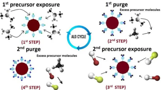
Atomic layer deposition (ALD) is a special type of vapor phase material deposition scheme that enables the conformal coating of thin films with sub-nanometer thickness control and excellent large-area uniformity. A unit ALD cycle consists of four steps: (i) exposure of metal-containing precursor, (ii) purge or evacuation, (iii) exposure of second precursor, and (iv) purge or evacuation. During the introduction of each precursor, surface reactions take place only at the available reactive sites, self-limiting the film growth to a
13
certain sub-monolayer thickness within a single ALD cycle. Evacuation/purging of excess precursor molecules and reaction by-products eliminates gas phase reactions and thus CVD-growth mode. Besides being ligand-preserving low temperature growth technique, its self-limiting characteristic offers precision thickness control at sub-ansgtrom level with superior conformality and uniformity over arbitrary topography, large areas, and complex stuctures. In this regard, ALD becomes an attractive low-temperature material growth method to be used for template-assisted fabrication of various nanostructured materials.[1], [2]
2.1.1 Mechanism
Figure 2.1 shows a schematic representation of a typical ALD cycle. Layer by layer material growth consists of following four steps:
(1) First precursor exposure, precursor chemisorbs on reactive sites with formation of reaction products.
(2) Unreacted excess precursor and reaction byproducts removal by purging the reactor with an inert gas.
(3) Second precursor exposure, precursor reacts with the 1st precursor which was chemisorbed on reactive sites with formation of reaction products.
(4) Unreacted excess precursor and reaction byproducts removal by purging the reactor with an inert gas.
14
Figure 2.1: Schematic representation of an ALD cycle consisting of four steps.
2.1.2 Factors Causing Saturation and Growth of Less than
Monolayer per Cycle
With the completion of one ALD cycle, amount of material deposited is called growth per cycle (GPC). There is a common misconception that ALD deposits one monolayer of material per cycle, however, reality is different i-e amount of material grown per cycle of ALD is less then a monolayer due to a effect known as “steric hindrance”. When a limited number of reactive sites are occupied by the reactants, a part of the surface is sheilded by the bulky ligands of precursor molecules making some of the reactive sites unavalaible to reactant molecules and resulting in less then monolayer GPC. Another possible reason of sub-monolayer GPC is the limited number of reactive sites in which the number of bonding sites is less than required to achieve a full ligand coverage. [1], [2]
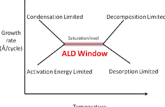
2.1.3 ALD Window
ALD window is the temperature range in which self-limiting growth occurs. In this temperature range, deposition has an ideal constant growth rate with
15
deposition of one monolayer per cycle. Center line (Fig. 2.2) indicates the ALD window on the growth rate vs. temperature graph. Deviation from ideal self-limiting ALD line corresponds to different mechanisms which prevent ALD to attain the requirement of self-limiting reactions.
There are two possible mechanisms below ALD window which correspond to non-self-terminating reactions. There can be condensation of precursor molecules at low temperatures resulting in high deposition rate. Incomplete reactions at low temperature will lead to low GPC.[1], [2]
On the other hand, at high temperatures, thermal decomposition causes a CVD-like growth mechanism in which gas phase decomposition of precursor molecules occur. In addition, deposition rate may be less at higher temperatures owing to desorption of sub-monolayer's deposited by ALD.[1], [2]
16
2.1.4 Merits and Demerits of ALD and Comparison with Other
Deposition Techniques
Table 2.1: Merits and demerits of ALD
Merits Demerits
Simple and accurate thickness control by changing the number of reaction cycles
Slow growth rate
Excellent conformality and uniformity Low precursor utilization efficiency
Atomic level control of material composition
High quality material deposition at low processing temperatures No need of reactant flux homogeneity, which enables large area and batch capability
Good reproducibility and straight forward scale-up
No gas phase reactions occur, favoring the usage of precursors that are highly reactive towards each other
Capability to prepare multilayer structures in a continuous process
Table 2.2: Comparison of ALD with other thin film deposition techniques.
Method ALD CVD MBE Sputter. Evapor. PLD Thickness Uniformity Good Good Fair Good Fair Fair
Film Density Good Good Good Good Good Good Step Coverage Good Varies Poor Poor Poor Poor Interface Quality Good Varies Good Poor Fair Varies Low Temp. Deposition Good Varies Good Good Good Good
Deposition Rate Poor Good Fair Good Good Good Lack of Pinholes Good Good Good Fair Fair Fair Automated Multilayers Good Fair Good Good Fair Fair Industrial Applicability Varies Good Varies Good Good Poor MBE= Molecular beam epitaxy, CVD= Chemical vapour deposition, and PLD- Pulsed laser deposition
17
2.1.5 Plasma vs. Thermal ALD
Exchange reactions between reactant molecules and chemisorb species can be sufficiently enhanced by using an external source of activation energy. Conventional mode of ALD (Thermal ALD) uses thermal energy to heat the entire reactor chamber of the substrate. One alternative of thermal ALD is plasma-enhanced ALD (PEALD) (also called as plasma-assisted ALD, PA-ALD), in which energetic radicals are generated to accelerate the self-terminating ALD reactions.
PA-ALD offers several merits over thermal ALD such as improved material properties,[31],[32] reduced growth temperatures,[33], [34] and increased choice of precursors and materials.[35] Mainly, these superior properties are the result of high reactivity provided by energetic radicals. Moreover, better control of stoichiometry, increased growth rate, minimized/eliminated nucleation delay, and increased process versatility have been reported due to higher degree of freedom in processing conditions (operating pressure, plasma power, plasma exposure time, etc.) of PA-ALD.[35] The major limitation of PEALD process is reduced conformality on high aspect ratio structures, which is believed to be due to recombination of radicals in deep trenches of high aspect ratio nanostructures.
2.2 InN and III-Nitride Alloy Thin Film
Deposition Using HCPA-ALD reactor
Among the III-nitride compound semiconductor materials family, InN has attracted much attention due to its largest electron saturation velocity, highest mobility, smallest direct band gap, and smallest electron effective mass. Electronic transport properties of InN reveal exceptionally high peak drift velocity at room temperature which makes it highly attractive potential candidate for high speed electronics.[3], [36], [37] Most thermodynamically favourable and stable phase of InN is hexagonal with wurtzite structure. Small
18
band gap value of InN has widened the spectral range covered by nitrides, from the ultraviolet for AlN to the near infrared for InN.
Significant progress has been made in the growth of hexagonal InN by different growth methods and among them, the most prominent methods are MBE[38], metal organic vapor phase epitaxy (MOVPE)[39], sputtering[40], and pulsed laser deposition[41].
Hexagonal wurtzite InN and GaN exhibit direct band gaps of 0.7 and 3.4 eV, respectively. Hence, ternary InxGa1-xN alloys provide band gap values which can be tuned from near ultraviolet to infrared range.[42] InxGa1-xN is a material of prime importance with its applications in InxGa1-xN/GaN based double heterostructure light emitting diodes (LEDs) and potential use in high-efficiency multi-junction thin film solar cells.[43] InxGa1-xN alloys are also considered as potential candidates for green LEDs with target wavelength of 525 nm. Green LEDs and deep UV LEDs are conceived as an important challenge in LED technology. Green LEDs with emission wavelength of 525 nm exhibit low efficiency compared to red and blue LEDs and this obstacle is known as the “Green gap”.[44] However, due to the considerable lattice mismatch between GaN and InN, there exists a solid phase miscibility gap in InxGa1-xN alloy system which is a significant hurdle in growing particularly In-rich InxGa1-xN films with decent crystalline quality.[45] Moreover, difference in formation enthalpies and vapor pressures of InN and GaN can lead to either low solubilities or surface segregation of indium in InxGa1-xN alloys.[46], [47]
A number of techniques have been utilized for the growth of InxGa1-xN films which include pulsed laser deposition,[48] MOCVD,[49] MBE,[50] sputtering[51], and hydride vapor phase epitaxy.[52] Among them, MOCVD and MBE are the leading epitaxial growth techniques to grow high quality single-crystalline InxGa1-xN thin films with very low impurity contents.
Hexagonal boron nitride (hBN) thin films have attracted special attention due to their useful properties such as wide band gap, high thermal conductivity, high oxidation resistance, and low surface energy.[53]–[55] On the other hand, GaN has been considered as one of the most important member of the III-nitride