Photonic band-gap effect, localization, and waveguiding in the two-dimensional Penrose lattice
Mehmet Bayindir,*E. Cubukcu, I. Bulu, and E. Ozbay Department of Physics, Bilkent University, Bilkent, 06533 Ankara, Turkey
共Received 9 February 2001; published 6 April 2001兲
We report experimental observation of a full photonic band gap in a two-dimensional Penrose lattice made of dielectric rods. Tightly confined defect modes having high quality factors were observed. Absence of the translational symmetry in Penrose lattice was used to change the defect frequency within the stop band. We also achieved the guiding and bending of electromagnetic waves through a row of missing rods. Propagation of photons along highly localized coupled-cavity modes was experimentally demonstrated and analyzed within the tight-binding approximation.
DOI: 10.1103/PhysRevB.63.161104 PACS number共s兲: 42.70.Qs, 42.60.Da, 61.44.Br, 71.15.Ap
Photonic crystals are artificial periodic structures in which the refractive index modulation gives rise to stop bands for electromagnetic waves 共EM兲 within a certain frequency range in all directions.1,2 The existence of photonic band gap3 and localized modes4 due to the Mie resonances5 and the Bragg scattering in these structures is of fundamental importance. Recently it was recognized that the photonic gaps can exist in two-dimensional共2D兲 quasicrystals.6–9 De-fect characteristics in the same structures were also investi-gated theoretically10and experimentally.11
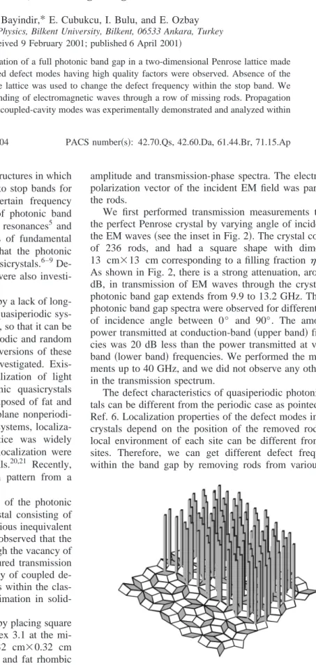
A quasiperiodic system is characterized by a lack of long-range periodic translational order. But the quasiperiodic sys-tem has long-range band orientational order, so that it can be considered as an intermediate between periodic and random systems.12–14 Previously, one-dimensional versions of these structures, the Fibonacci lattices, were investigated. Exis-tence of photonic stop bands15 and localization of light waves16 in these one-dimensional photonic quasicrystals were reported. The Penrose tiles17 are composed of fat and skinny rhombic unit cells and fill the 2D plane nonperiodi-cally as illustrated in Fig. 1. In electronic systems, localiza-tion phenomena in the 2D Penrose lattice was widely studied.18,19 Moreover, spectral gaps and localization were observed in 2D acoustical Penrose crystals.20,21 Recently, Krauss et al. demonstrated the diffraction pattern from a grating based on Penrose tiles.22
In this paper, we report on observation of the photonic band-gap effect in a 2D Penrose quasicrystal consisting of dielectric rods. Defect characteristics of various inequivalent sites of the crystal were investigated. It is observed that the EM waves can be guided and bended through the vacancy of removed rods along a line. We also measured transmission spectrum and dispersion relation of an array of coupled de-fects, and analyzed the experimental results within the clas-sical wave analog of tight-binding approximation in solid-state physics.23
The 2D Penrose lattice was constructed by placing square shaped alumina rods, having refractive index 3.1 at the mi-crowave frequencies and dimensions 0.32 cm⫻0.32 cm ⫻15.25 cm, at each vertice of the skinny and fat rhombic cells共Fig. 1兲. The edge of each rhombus is a⫽1.2 cm. The experimental setup consists of a HP 8510C network analyzer and microwave horn antennas to measure the
transmission-amplitude and transmission-phase spectra. The electric-field polarization vector of the incident EM field was parallel to the rods.
We first performed transmission measurements through the perfect Penrose crystal by varying angle of incidence of the EM waves共see the inset in Fig. 2兲. The crystal consisted of 236 rods, and had a square shape with dimensions 13 cm⫻13 cm corresponding to a filling fraction ⬃0.14. As shown in Fig. 2, there is a strong attenuation, around 50 dB, in transmission of EM waves through the crystal. The photonic band gap extends from 9.9 to 13.2 GHz. The same photonic band gap spectra were observed for different values of incidence angle between 0° and 90°. The amount of power transmitted at conduction-band共upper band兲 frequen-cies was 20 dB less than the power transmitted at valence-band 共lower band兲 frequencies. We performed the measure-ments up to 40 GHz, and we did not observe any other gaps in the transmission spectrum.
The defect characteristics of quasiperiodic photonic crys-tals can be different from the periodic case as pointed out in Ref. 6. Localization properties of the defect modes in quasi-crystals depend on the position of the removed rod, since local environment of each site can be different from other sites. Therefore, we can get different defect frequencies within the band gap by removing rods from various
posi-FIG. 1. Schematic drawing of a two-dimensional Penrose pho-tonic crystal. The dielectric rods are placed at all vertices of fat and skinny rhombic cells.
RAPID COMMUNICATIONS
PHYSICAL REVIEW B, VOLUME 63, 161104共R兲
tions. This feature might be important for certain applications.24,25
We measured the transmission spectrum through a Pen-rose crystal, which consisted of 98 rods, with a single rod removed defect as labeled in the inset of Fig. 3. Each defect has different local properties, i.e., number and arrangement of neighboring rods. As shown in Fig. 3, we observed strongly localized cavity modes within the stop band of the crystal. The corresponding defect frequencies were fA ⫽11.436 GHz, fB⫽11.301 GHz, and fC⫽10.679 GHz. The quality factors, defined as center frequency divided by the peak’s full width at half maximum, of these cavities were measured to be QA⫽817, QB⫽513, and QC⫽305.
Guiding and bending of EM waves in 2D periodic photo-nic crystals were theoretically demonstrated by Mekis
et al.26 and observed experimentally by Lin and
co-workers.27These phenomena was recently reported in 2D octagonal quasicrystals.7,10In order to demonstrate the guid-ing and bendguid-ing of the EM waves, we removed a row of rods from the Penrose lattice共see right panels in Fig. 4 for wave-guide geometries兲. The transmission spectra corresponding to a straight共upper-right panel兲 and 90° bended 共lower-right panel兲 waveguides were measured and displayed in Figs. 4共a兲 and 4共b兲, respectively. For the straight waveguide, we observed guiding of EM waves from 10.60 to 13.22 GHz. For the bended waveguide, we achieved bending of EM waves from 10.60 to 13.06 GHz. The underlying physics of such waveguides can be investigated within the slab wave-guide model, where the both crystals around the array of missing rods act as mirrors. Therefore, we expect that the EM wave to be guided through the introduced gap starting from a cutoff frequency, resonant frequency of the Fabry-Perot cavity, which depends on the width of the gap.28
Recently, we have reported a new type of propagation mechanism through an array of coupled cavities in one-dimensional structures,29 and three-dimensional layer-by-layer photonic crystals.30,31This mechanism depends on the coupling of each localized cavity mode with its neighbors, and therefore the EM energy can be transferred along the defect sites. In a periodic system, local properties of defect sites are the same, and we can represent each localized defect mode by a single function E⍀(r). Therefore, the waveguid-ing mode along the coupled-cavity array satisfies the Bloch condition. Can we observe this type of waveguiding in a quasiperiodic system? To demonstrate these phenomena, we looked for a path on the Penrose lattice along which all de-fect sites were identical. Such a path is illustrated in Fig. 5 共right panel, dotted line兲. There is a localized EM mode around each missing rod that is surrounded by seven neigh-boring rods.
We measured the transmission of EM waves through this
FIG. 2. Transmission characteristics of a Penrose dielectric crys-tal for various incidence angles. A stop band extending from 9.9 to 13.2 GHz was observed irrespective of the incidence angle. Inset: The (䊉) symbols denote vertices of the Penrose lattice.
FIG. 3. Defect characteristics of a Penrose crystal consisting of 98 dielectric rods obtained by removing a single rod from various locations. Highly localized defect modes were observed. Since the crystal has many inequivalent defect sites, we can change the defect frequency within the stop band. The inset shows location of the defects. Here, point B is positioned at the center of the crystal.
FIG. 4. 共a兲 Waveguiding through a straight waveguide which was constructed by removing one row of rods (䊊symbols兲 from the perfect Penrose crystal. 共b兲 Bending of EM wave through a 90° sharp bend. The right panels show schematics of the straight and bended waveguides.
RAPID COMMUNICATIONS
MEHMET BAYINDIR, E. CUBUKCU, I. BULU, AND E. OZBAY PHYSICAL REVIEW B 63 161104共R兲
coupled-cavity array, that consisted of nine defect sites关Fig. 5共a兲兴. We observed that a defect band, waveguiding band, was formed within the photonic band gap. The guiding band extended from 10.25 to 11.38 GHz. The maximum transmis-sion in the waveguiding band did not reach unity in contrast to what we had observed in 3D photonic crystals.30,31This can be explained by the absence of confinement of the EM waves along the vertical direction共along the rod axis兲,32that resulted in leakage of EM waves along this direction.
The dispersion relation of the coupled-cavity structure can be obtained from transmission-phase measurements.31,33,34 By using the net phase difference ␦ between the phase of the EM wave propagating through the photonic crystal and the phase of the EM wave propagating in free space, we can determine the wave vector k of the crystal as a function of frequency from
k⌳⫽␦⌳/L⫹2⌳/c, 共1兲
where c is the speed of the light,⌳⫽2.28 cm is the distance between two consecutive defects, and L⫽20.6 cm is the
to-tal crysto-tal thickness.
The dispersion relation can also be determined within the TB approximation31which is given by
k⯝⍀关1⫹cos共k⌳兲兴, 共2兲
where ⍀⫽10.85 GHz is the resonance frequency corre-sponding to a single defect,⬃⫺0.05 is a TB parameter that was experimentally determined from the splitting of two coupled cavities and the width of waveguiding band.30 Fig-ure 5共b兲 shows the comparison of the measured (〫 sym-bols兲 and the calculated 共solid line兲 dispersion relations. The good agreement between the experiment and the theory is an indication of the usefulness of the TB scheme in quasiperi-odic photonic structures.
At this point it is natural to ask the following question. Can we observe photonic band gaps and the waveguiding phenomena in the absence of periodicity? The answer is yes. We have observed that the photonic band gap and metallicity gap persist even if large amount of positional disorder was introduced in 2D dielectric and metallic photonic crystals, respectively. It was also observed that the defect frequency of a single rod removed cavity can be tuned by changing position of the defect sites in weakly disordered 2D dielectric and metallic photonic crystals. Waveguiding was also achieved for weakly disordered systems.35
In conclusion, we have experimentally observed that the EM waves cannot propagate within a certain frequency range through a 2D quasicrystal that was composed of the Penrose tiling of dielectric rods. It was demonstrated that by remov-ing a sremov-ingle rod from an otherwise perfect Penrose lattice, we could create a highly localized cavity mode. Since the crystal had many inequivalent sites, we achieved different defect frequencies within the photonic band gap. Moreover, we demonstrated guiding and bending of the EM waves along a row of missing rods. Particular attention was devoted to the transferring of the EM energy through a coupled-cavity ar-ray. Using a theory based on the tight-binding approxima-tion, we obtained good agreement between the measured and the calculated dispersion relations.
This work was supported by NATO Grant No. SfP971970, National Science Foundation Grant No. INT-9820646, Turkish Department of Defense Grant No. KOBRA-001, and Thales JP8.04.
*Author to whom correspondence addressed. Electronic address: [email protected]
1J. D. Joannopoulos, R. D. Meade, and J. N. Winn, Photonic Crys-tals: Molding the Flow of Light 共Princeton University Press, Princeton, NJ, 1995兲.
2For a recent review, see articles in Photonic Band Gap Materials, edited by C. M. Soukoulis共Kluwer, Dortrecht, 1996兲.
3E. Yablonovitch, Phys. Rev. Lett. 58, 2059共1987兲. 4S. John, Phys. Rev. Lett. 58, 2486共1987兲.
5C. F. Bohren and D. R. Huffman, Absorption and Scattering of Light by Small Particles共Wiley, New York, 1983兲, Chap. 4.
6Y. S. Chan, C. T. Chan, and Z. Y. Liu, Phys. Rev. Lett. 80, 956 共1998兲.
7C. Jin, B. Cheng, B. Man, Z. Li, and D. Zhang, Appl. Phys. Lett. 75, 1848共1999兲.
8M. E. Zoorob, M. D. B. Charlton, G. J. Parker, J. J. Baumberg, and M. C. Netti, Nature共London兲 404, 740 共2000兲.
9X. Zhang, Zhao-Quing Zhang, and C. T. Chan, Phys. Rev. B 63, 081105共R兲 共2001兲.
10S. S. M. Cheng, Lie-Ming Li, C. T. Chan, and Z. Q. Zhang, Phys. Rev. B 59, 4091共1999兲.
11C. Jin, B. Cheng, B. Man, Z. Li, and D. Zhang, Phys. Rev. B 61,
FIG. 5. 共a兲 Transmission of EM waves through an array of coupled cavities which is shown in the right panel. The䊊 symbols represent the missing rods. Photons can propagate along these lo-calized coupled defect modes throughout a waveguiding band ex-tending from 10.25 to 11.38 GHz.共b兲 Measured (〫 symbols兲 and calculated共solid line兲 dispersion relations. The experimental result is in good agreement with the tight-binding prediction.
RAPID COMMUNICATIONS
PHOTONIC BAND-GAP EFFECT, LOCALIZATION, AND . . . PHYSICAL REVIEW B 63 161104共R兲
10 762共2000兲.
12D. Levine and P. J. Steinhardt, Phys. Rev. B 34, 596共1986兲. 13P. J. Steinhardt and S. Ostlund, The Physics of Quasicrystals
共World Scientific, Singapore, 1987兲.
14C. Janot, Quasicrystals: A Primer 共Clarendon Press, Oxford, 1994兲.
15T. Hattori, N. Tsurumachi, S. Kawato, and H. Nakatsuka, Phys. Rev. B 50, R4220共1994兲.
16W. Gellermann, M. Kohmoto, B. Sutherland, and P. C. Taylor, Phys. Rev. Lett. 72, 633共1994兲.
17R. Penrose, Bull. Inst. Math. Appl. 10, 266共1974兲; M. Gardner, Sci. Am. 236, 110共1977兲.
18M. Kohmoto and B. Sutherland, Phys. Rev. Lett. 56, 2740共1986兲. 19J. Vidal, R. Mosseri, and B. Doucot, Phys. Rev. Lett. 81, 5888
共1998兲.
20S. He and J. D. Maynard, Phys. Rev. Lett. 62, 1888共1989兲. 21F. M. de Espinosa and M. Torres, Appl. Phys. Lett. 65, 1352
共1994兲.
22T. F. Krauss and R. M. De La Rue, Prog. Quantum Electron. 23, 51共1999兲.
23N. W. Ashcroft and N. D. Mermin, Solid State Physics共Saunders, Philadelphia, 1976兲, p. 175.
24P. R. Villeneuve, D. S. Abrams, S. Fan, and J. D. Joannopoulos, Opt. Lett. 21, 2017共1996兲; P. R. Villeneuve, S. Fan, and J. D. Joannopoulos, Phys. Rev. B 54, 7837共1996兲.
25S. Noda, A. Chutinan, and M. Imada, Nature共London兲 407, 608 共2000兲.
26A. Mekis et al., Phys. Rev. Lett. 77, 3787共1996兲.
27Shawn-Yu Lin, E. Chow, V. Hietala, P. R. Villeneuve, and J. D. Joannopoulos, Science 282, 274共1998兲.
28B. Temelkuran and E. Ozbay, Appl. Phys. Lett. 74, 486共1999兲. 29
Mehmet Bayindir, S. Tanriseven, and E. Ozbay, Appl. Phys. A: Mater. Sci. Process. 72, 117共2001兲.
30Mehmet Bayindir, B. Temelkuran, and E. Ozbay, Phys. Rev. Lett. 84, 2140共2000兲, and references therein.
31Mehmet Bayindir, B. Temelkuran, and E. Ozbay, Phys. Rev. B 61, R11 855共2000兲.
32S. G. Johnson, P. R. Villeneuve, S. Fan, and J. D. Joannopoulos, Phys. Rev. B 62, 8212共2000兲.
33W. M. Robertson et al., Phys. Rev. Lett. 68, 2023共1992兲. 34E. Ozbay et al., Opt. Lett. 19, 1155共1994兲.
35Mehmet Bayindir, E. Cubukcu, I. Bulu, and E. Ozbay 共unpub-lished兲.
RAPID COMMUNICATIONS
MEHMET BAYINDIR, E. CUBUKCU, I. BULU, AND E. OZBAY PHYSICAL REVIEW B 63 161104共R兲