Giant Modal Gain Coe
fficients in Colloidal II−VI Nanoplatelets
Burak Guzelturk,
*
,†,‡Matthew Pelton,
§Murat Olutas,
‡,∥and Hilmi Volkan Demir
⊥,‡†Stanford Institute for Materials and Energy Sciences, SLAC National Accelerator Laboratory, Menlo Park, California 94025, United States
‡Department of Electrical and Electronics Engineering, Department of Physics, UNAM - Institute of Materials Science and Nanotechnology, Bilkent University, Ankara 06800 Turkey
§Department of Physics, University of Maryland, Baltimore County, Baltimore, Maryland 21250, United States ∥Department of Physics, Bolu Abant Izzet Baysal University, Bolu 14030, Turkey
⊥Luminous! Center of Excellence for Semiconductor Lighting and Displays, School of Electrical and Electronic Engineering, School of Physical and Mathematical Sciences, School of Materials Science and Engineering, Nanyang Technological University, Nanyang Avenue, Singapore 639798, Singapore
*
S Supporting InformationABSTRACT: Modal gain coefficient is a key figure of merit for a laser material. Previously, net modal gain coefficients larger than a few thousand cm−1were achieved in II−VI and III−V semiconductor gain media, but this required operation at cryogenic temperatures. In this work, using pump- fluence-dependent variable-stripe-length measurements, we show that colloidal CdSe nanoplatelets enable giant modal gain coefficients at room temperature up to 6600 cm−1 under pulsed optical excitation. Furthermore, we show that excep-tional gain performance is common to the family of CdSe nanoplatelets, as shown by examining samples having different vertical thicknesses and lateral areas. Overall, colloidal II−VI nanoplatelets with superior optical gain properties are
promising for a broad range of applications, including high-speed light amplification and loss compensation in plasmonic photonic circuits.
KEYWORDS: Colloidal nanoplatelets, colloidal quantum wells, CdSe, modal gain coefficient, variable stripe length method, optical gain
O
ver the past decade, colloidal CdSe nanoplatelets (NPLs), also alternatively known as colloidal quantum wells, joined the family of II−VI semiconductor nanocrystals as a promising new member1and have attracted great interest for optoelectronic applications owing to their superior optical properties, including spectrally narrow photoluminescence,2 strong light absorption,3and polarized light emission.4Recent reports5−12identified a key application for NPLs as gain media for optically pumped lasers. To date, NPL heterostructures exhibited remarkable optical gain performance, including low gain thresholds5(∼8 μJ/cm2) and long gain lifetimes13(∼400 ps). Moreover, initial reports showed appreciably large modal gain coefficient (∼650 cm−1)5,6 in the NPLs, significantly larger than those found for conventional quantum dots.14,15Modal gain coefficient is an important benchmarking parameter for a gain medium and quantifies how much light is amplified per unit length. CdSe NPLs possess significantly large linear3,16and nonlinear17,18absorption cross-sections due to their giant oscillator strength.19This suggests the possibility of a large stimulated emission cross-section and associated large modal gain coefficients. However, the limits of optical
gain using CdSe NPLs have not been elucidated to date. Here we show that CdSe NPLs attain giant net modal gain coefficients as high as ∼6600 cm−1 at room temperature.
This net modal gain exceeds those reported for any other gain media at room temperature so far. This makes these solution processable NPLs highly attractive for applications that require high modal gain, such as lossy plasmonic photonic structures20 and parity-time-symmetric photonic designs.21
In this work, we synthesized CdSe NPLs with different vertical thicknesses and lateral areas based on previous recipes.2,17,22 In Figure 1, we show optical absorption and photoluminescence (PL) spectra of CdSe NPLs that have 4 monolayer (ML) vertical thickness. The two absorption peaks at 511 and 480 nm are due to excitonic absorption associated with electron-heavy hole and electron-light hole transitions, respectively.2 The absorption profile shows a steplike density
Received: September 26, 2018 Revised: December 11, 2018 Published: December 12, 2018
pubs.acs.org/NanoLett
of states due to one-dimensional quantum confinement in these materials.17The PL peak is at 513 nm (when the NPLs are dissolved in toluene) and the emission profile is quite narrow (with a full width at half-maximum of∼8 nm at room temperature) due to atomically flat surfaces and atomic-level monodispersity in thickness.23 Figure 1b shows a high-angle annular dark-field scanning transmission electron microscopy (HAADF-STEM) image of the 4 monolayer thick CdSe NPLs. For this batch of sample, wefind the average lateral size to be 9 nm by 12 nm and the vertical thickness to be∼1.2 nm (see inset ofFigure 1b).
We make solid thin films by spin-coating the NPLs on precleaned 1 cm by 1 cm quartz substrates to study amplified spontaneous emission (ASE). The postsynthesis cleaning procedure has been optimized, which allowed us to prepare NPL solid films that are close-packed and free of excess ligands. Thefilm thickness of the samples studied here is ∼200 nm. When the NPLs form a close-packed solidfilm, their PL peak redshifts to 518−522 nm and the emission line width increases to 15 nm. This redshift and broadening could arise from an increase in the effective dielectric function surrounding the NPLs, which would increase the dielectric screening and lead to inhomogeneous broadening. In addition, densely packed NPL thin-films could favor the formation of excimer states,24which exhibit a red-shifted emission peak as compared to that of the free exciton emission. We excite the samples in a stripe geometry by focusing the pump beam via a cylindrical lens. We used a pulsed Ti:sapphire femtosecond laser (SpectraPhysics, Spitfire Pro) to excite the samples. The output of the laser is frequency doubled using a BBO crystal. The excitation photon energy is 3.1 eV, the pulse width is ∼150 fs, and the repetition rate is 1 kHz. Emission from the NPLs is detected by afiber-coupled spectrometer and the fiber is positioned close the edge of the sample.Figure 2a shows the evolution of the emission spectrum as a function of the pump fluence. As the pump fluence is increased, a new peak rises at 532 nm, which is due to ASE and indicates the presence of net optical gain in the material. The ASE peak is red-shifted as compared to the PL peak, which is consistent with previous reports suggesting biexcitons as the gain active species in the NPLs.7,25 Figure 2b depicts the integrated emission intensity versus pump fluence marking the ASE threshold, which happens when the modal gain becomes equal to the loss of the system. In this sample, wefind the ASE threshold to be 13 μJ/cm2, which is on par with the best previous report in CdSe
NPLs7 and is within a factor of 3 as compared to the best reports in colloidal nanocrystals (e.g., cesium lead halide perovskite nanocrystals26and giant-shell CdSe/CdS quantum dots27) to date.
Now we turn our focus to net modal gain coefficients measured by the variable stripe length (VSL) method,28,29 which has been commonly employed to characterize modal gain in a broad range of solid-state gain media such as quantum dots,15 organic semiconductors,30 and single-crystal bulk Figure 1.(a) Absorbance and photoluminescence spectra (normalized) and (b) HAADF-STEM image of CdSe nanoplatelets (NPLs) having 4 ML vertical thickness. The inset in (b) shows a high-resolution TEM cross-section image of a 4 ML thick NPL.
Figure 2.(a) Emission spectra of a thinfilm of CdSe nanoplatelets (NPLs) under increasing pumpfluence. An amplified spontaneous emission (ASE) peak emerges at 532 nm when thefluence is above 13 μJ/cm2. (b) Integrated emission intensity versus pump fluence showing a threshold behavior and transition from spontaneous photoluminescence to ASE. Inset shows the integrated emission intensity over a larger excitationfluence range.
materials.31As shown inFigure 3a, the sample is excited in a stripe geometry, and we change the stripe length via a tunable slit. To minimize diffraction effects,32 the slit is positioned close to the sample (∼5 mm). To ensure that the stripe begins from the edge of the sample, one side of the slit isfixed while the other side is moved. Figure 3b shows the integrated emission intensity (in log-scale) as a function of the stripe length measured under four different pump intensities. Net gain in the sample provides amplification along the stripe direction, hence the integrated emission intensity increases exponentially as a function of the stripe length. This relationship is commonly expressed as28
= − I l A g e ( ) ( g l 1) emission net net (1) α = − gnet gmodal (2)
where l is the stripe length, A is the spontaneous emission growth parameter, gnetis the net modal gain coefficient, gmodalis
the modal gain coefficient, and α is the waveguide loss coefficient. Fits using eq 1match well with the experimental data (seeFigure 3b). For example, wefind gnetto be 163± 10 cm−1 at a fluence of 17 μJ/cm2. As the pump fluence is increased, the integrated emission intensity starts to rise at a faster rate. This implies that gnetrises as the pump intensity is
increased. For example, wefind gnetto be 6300± 300 cm−1at 910μJ/cm2.
Figure 3c shows the evolution of net modal gain, gnet, as a
function of the pump fluence. Here, the average of four different measurements on the same sample for each pump intensity is considered to provide statistics, as highlighted via error bars inFigure 3c. At low pumpfluences (15−60 μJ/cm2), gnet increases linearly as a function of the fluence, whereas
above this level gnetstarts to deviate from the linear relationship
and saturates which is consistent with the integrated emission intensity from the sample shown in the inset ofFigure 2b. This behavior can befitted by a saturation curve (see Figure 3c) with a saturationfluence of 195 μJ/cm2. The maximum gnetis
as high as 6600± 350 cm−1.
To validate these giant modal gain coefficients, we reconsider the constraints of the VSL method. Equation 1is valid when the modal gain of the material is independent of the stripe length. However, in the case of very large gain, ASE itself can deplete the population inversion within the excitation stripe, hence integrated emission intensity may saturate as the stripe length is increased. Previous reports33,34 showed that saturation length (Lsat) times net modal gain (Lsat× gnet) is on
the order of ∼10. Thus, when gnet is 5000 cm−1, one could
expect Lsatto be on the order of∼20 μm. Because of this,eq 1
would be valid only for a short-range of stripe lengths before the emitted intensity saturates as a function of the stripe length. To understand this point better, we also considered a full analytical form derived by Cerdán et al.,35
which takes into account the stripe length dependent saturation (see SI). We Figure 3.(a) Schematic representation of the experimental setup for the VSL measurements. (b) Integrated emission intensity (log-scale) from the sample as a function of the stripe length forfive different pump intensities. Fits are performed usingeq 1. (c) Net modal gain coefficient as a
function of the pumpfluence. A saturation curve fits the experimental data with a saturation fluence of 195 μJ/cm2. The maximum net modal gain is measured to be∼6600 cm−1. (d) Modal gain spectra measured atfive different pump intensities and fitted by Gaussian functions.
fitted the same experimental data for the highest pump intensity case using both the full analytical form (eq S2) andeq 1 (seeFigure S1). The full analytical form gives gnet = 6530 cm−1, which is in very good agreement with the value of gnet
fitted byeq 1. When usingeq 1, we limited the stripe length span to∼40 μm to stay away from the saturation region.
We also frequency-resolve the net modal gain coefficients (seeFigure 3d) forfive different pump fluences. Here, gnet(λ)
follows the ASE profile, as expected. The gnetspectrum slightly redshifts (from 532 to 536 nm) and broadens (from 11 to 13 nm) as the pump fluence is increased. This redshift at increased excitation fluence is likely to originate from many-body Coulomb interactions causing band gap renormalization and electron−hole plasma screening, as previously observed in epitaxial quantum-well-based gain media.36 The narrow bandwidth of the gain even at very high pump intensity is an important feature enabling giant modal gain coefficients in these NPLs, because a large density of population inversion (i.e., multiple biexcitons per NPL) can be generated and sustained in a highly concentrated spectral region.
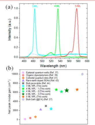
We also investigate the net modal gain coefficients in CdSe NPLs having different vertical thickness and lateral area.Figure 4a shows the ASE spectra of NPLs having 3, 4, and 5 ML
thickness with ASE peaks at 480, 532, and 575 nm, respectively. The optical gain covers an important range falling within the “green gap” region, which has been difficult to access with conventional epitaxial semiconductor materials. Via heterostructuring and alloying of the NPLs, the spectral gain coverage could be extended even further.37,38In addition, we
study 4 ML thick NPLs with different lateral extent (4 ML NPL-1: 9 nm by 11 nm; 4 ML NPL-2: 11 nm by 14 nm; and 4 ML NPL-3: 14 nm by 18 nm), to check the dependence of the maximum achievable net modal gains on the lateral area. We perform VSL measurements on these different NPL samples (seeSIfor the VSL curves measured in the high-fluence range and respective fits using eq 1). Among different vertical thickness NPLs, the 3 ML thick one exhibits the smallest gnetof about 2400 cm−1. Smaller modal gain in the 3 ML sample is mainly associated with its poor stability, where the ASE peak intensity immediately starts decreasing when the pumpfluence is above the ASE threshold. On the other hand, encapsulated 4 and 5 ML NPL samples exhibited significantly improved stability. Under an excitationfluence of 30 μJ/cm2, the ASE peak remained stable for 60 min under continuous exposure to the pump, whereas the ASE peak was stable for 3 min under an excitation fluence of 1 mJ/cm2. Among 4 ML samples with different lateral areas, we also do not see any significant difference in the maximum gnet. Also, 5 ML sample exhibited a
maximum gnetthat is very similar to that of the 4 ML samples. These indicate that stable NPLs (both 4 and 5 ML thick ones) offer giant modal gain independent of their vertical thickness and lateral area. Overall, the maximum measured gnetis∼6600
cm−1.
Figure 4b shows the maximum gnetachieved in these NPL
samples along with maximum gnet measured in other material
systems. Previously, II−VI (e.g., CdS and ZnO)39and III−V (e.g., GaN31an InGaAsP40,41) semiconductor materials in their bulk form exhibited very large modal gain up to 10,000 cm−1,31 but these were all measured at low temperatures (T < 10 K). Quantum confined epitaxial systems such as III−V quantum wells42 and dots43 were shown to exhibit modal gain in the range of 10 to ∼100 cm−1, although their intrinsic material gain can be very large (>10,000 cm−1). Organic gain media such as organic dyes44and conjugated polymers45also offered limited modal gain up to 350 cm−1. In colloidal quantum dots and nanorods, the maximum gnet was reported15,46,47 to be
∼600 cm−1. Semiconductor optical amplifiers based on rare
earth-doped glasses48 showed relatively large modal gains reaching a level of 2400 cm−1(∼1000 dB/cm for an amplifier length of 25 μm). More recently, polycrystalline methyl-ammonium lead halide perovskite thin-films49 showed a net modal gain of 3000 cm−1. To the best of our knowledge, colloidal CdSe NPLs attain the largest net modal gain coefficient measured at room temperature among any other optical gain system reported so far.50
Spectrally narrow and giant modal gain was theoretically predicted for strongly quantum confined systems by Asada et al.51but was not previously possible to achieve using colloidal quantum dots. To date, colloidal quantum dots suffered from small modal gain coefficients due to short-lived gain associated with nonradiative Auger recombination.52 In addition, the material gain was small in these quantum dots, because the QDs cannot support multiple excitons at their band edges. Because of this, modal gain coefficients for these materials saturate at pump intensities approximately twice the net gain threshold.27On the other hand, NPLs can sustain large gain even at much higher pump levels (∼2 orders of magnitude above the net gain threshold). This indicates that material gain (gmat) is also large: gnet = Γ × gmat, where Γ is the mode
confinement factor. In the thin films having high volume packing density, we estimate53Γ to be 0.43 by considering the thickness of thefilm (∼200 nm, seeFigure S3) and its effective Figure 4. (a) Amplified spontaneous emission (ASE) spectra of
nanoplatelets (NPLs) with 3, 4, and 5 ML vertical thickness. (b) Peak net modal gain coefficients in the NPLs with different vertical thicknesses and lateral areas. Peak net modal gains reported in other systems are also compared here. The empty symbol indicates a measurement at cryogenic temperatures.
refractive index (∼1.754). Thus, the material gain of the NPL thin-film at room temperature is ∼15,300 cm−1, which is comparable to the best gain systems of bulk GaN31and GaAs43 with material gains estimated to be∼20,000 cm−1at cryogenic temperatures. It is also on par with the best epitaxial quantum dot systems (e.g., InAs/GaAs55) with a material gain of 15,000 cm−1 at room temperature.50 A recent communication also agrees well with the existence of large material gain in CdSe NPLs.56
From the application point of view, excitation pulse duration is an important parameter. Although continuous-wave (CW) or quasi-CW pumping is desired for practical applications, short-lived gain (<10 ps) has posed a significant limitation in conventional quantum dot-based gain systems.57CdSe NPLs have shown significantly longer gain lifetimes, ranging from 1509to 400 ps,13hence quasi-CW pumping is expected to be within reach for the NPLs. Indeed, recent reports including refs 7 and 10 showed that CW lasing is possible using the NPL-based gain media. This indicates that large intrinsic gain can be sustained under CW pumping, and Auger recombina-tion is less detrimental as compared to convenrecombina-tional colloidal quantum dots. Under CW operation, heat dissipation and material stability would become important factors toward a sustainable optical gain.58
Overall, colloidal NPLs can reach a high density of population inversion, which indicates that each NPL can sustain multiple gain-active excitonic species. This suggests that multiexcitonic optical gain is extremely stable and nonradiative annihilation of biexcitons is minimized. The saturation effect in Figure 3c can be attributed to either a phase-space filling effect, where the maximum number of biexcitons that can simultaneously survive within a NPL is limited due to the Pauli exclusion principle as predicted by Miller et al.,59or to exciton dissociation at high densities due to a Mott transition.60
In conclusion, NPLs combine the advantageous aspects of both colloidal systems (i.e., large mode confinement factor) and epitaxial semiconductors (i.e., large intrinsic material gain) and provide giant modal gain coefficients at room temperature. These materials possess high band-edge density of states and large exciton binding energies, allowing for highly efficient excitonic gain. Unlike in conventional colloidal quantum dots, exciton−exciton interactions are relatively unimportant in NPLs, simply because the spatial exciton density required for gain is lower. Importantly, solution processability of the NPLs means that they can be integrated into arbitrary substrates, which allows in principle for low-cost device fabrication and ease of processing. In addition, superior optical gain perform-ance of these NPLs makes them exciting prospects for CW pumped colloidal lasers as well as for electrical injection.
■
ASSOCIATED CONTENT*
S Supporting InformationThe Supporting Information is available free of charge on the ACS Publications website at DOI: 10.1021/acs.nano-lett.8b03891.
Full analytical form of thefitting function for the VSL data, comparison of the VSL fits using full form versus classical form, and VSL data measured using the samples mentioned in the main text (PDF)
■
AUTHOR INFORMATIONCorresponding Author
*E-mail:[email protected]. Phone.: +1 650 561 2481.
ORCID
Burak Guzelturk:0000-0003-1977-6485
Matthew Pelton:0000-0002-6370-8765
Hilmi Volkan Demir:0000-0003-1793-112X Notes
The authors declare no competingfinancial interest.
■
ACKNOWLEDGMENTSWe gratefully acknowledge financial support from the Singapore National Research Foundation under the programs of NRF-NRFI2016-08. H.V.D. also acknowledges support from ESF-EURYI and TUBA.
■
REFERENCES(1) Ithurria, S.; Dubertret, B. J. Am. Chem. Soc. 2008, 130 (49), 16504−16505.
(2) Ithurria, S.; Tessier, M. D.; Mahler, B.; Lobo, R. P. S. M.; Dubertret, B.; Efros, A. L. Nat. Mater. 2011, 10 (12), 936−941.
(3) Yeltik, A.; Delikanli, S.; Olutas, M.; Kelestemur, Y.; Guzelturk, B.; Demir, H. V. J. Phys. Chem. C 2015, 119 (47), 26768−26775.
(4) Gao, Y.; Weidman, M. C.; Tisdale, W. A. Nano Lett. 2017, 17 (6), 3837−3843.
(5) She, C.; Fedin, I.; Dolzhnikov, D. S.; Demortière, A.; Schaller, R. D.; Pelton, M.; Talapin, D. V. Nano Lett. 2014, 14 (5), 2772−2777. (6) Guzelturk, B.; Kelestemur, Y.; Olutas, M.; Delikanli, S.; Demir, H. V. ACS Nano 2014, 8 (7), 6599−6605.
(7) Grim, J. Q.; Christodoulou, S.; Di Stasio, F.; Krahne, R.; Cingolani, R.; Manna, L.; Moreels, I. Nat. Nanotechnol. 2014, 9 (11), 891−895.
(8) Kelestemur, Y.; Guzelturk, B.; Erdem, O.; Olutas, M.; Gungor, K.; Demir, H. V. H. V. Adv. Funct. Mater. 2016, 26 (21), 3554.
(9) She, C.; Fedin, I.; Dolzhnikov, D. S.; Dahlberg, P. D.; Engel, G. S.; Schaller, R. D.; Talapin, D. V. ACS Nano 2015, 9 (10), 9475− 9485.
(10) Yang, Z.; Pelton, M.; Fedin, I.; Talapin, D. V.; Waks, E. Nat. Commun. 2017, 8 (1), 143.
(11) Li, M.; Zhi, M.; Zhu, H.; Wu, W.-Y.; Xu, Q.-H.; Jhon, M. H.; Chan, Y. Nat. Commun. 2015, 6, 8513.
(12) Pelton, M. J. Phys. Chem. C 2018, 122 (20), 10659−10674. (13) Guzelturk, B.; Kelestemur, Y.; Olutas, M.; Li, Q.; Lian, T.; Demir, H. V. J. Phys. Chem. Lett. 2017, 8 (21), 5317.
(14) Guzelturk, B.; Kelestemur, Y.; Gungor, K.; Yeltik, A.; Akgul, M. Z. M. Z.; Wang, Y.; Chen, R.; Dang, C.; Sun, H.; Demir, H. V. H. V. Adv. Mater. 2015, 27 (17), 2741−2746.
(15) Malko, A. V.; Mikhailovsky, A. A.; Petruska, M. A.; Hollingsworth, J. A.; Htoon, H.; Bawendi, M. G.; Klimov, V. I. Appl. Phys. Lett. 2002, 81 (7), 1303.
(16) Achtstein, A. W.; Antanovich, A.; Prudnikau, A.; Scott, R.; Woggon, U.; Artemyev, M. J. Phys. Chem. C 2015, 119, 20156− 20161.
(17) Olutas, M.; Guzelturk, B.; Kelestemur, Y.; Yeltik, A.; Delikanli, S.; Demir, H. V. H. V. ACS Nano 2015, 9 (5), 5041−5050.
(18) Scott, R.; Achtstein, A. W.; Prudnikau, A.; Antanovich, A.; Christodoulou, S.; Moreels, I.; Artemyev, M.; Woggon, U. Nano Lett. 2015, 15, 4985.
(19) Naeem, A.; Masia, F.; Christodoulou, S.; Moreels, I.; Borri, P.; Langbein, W. Phys. Rev. B: Condens. Matter Mater. Phys. 2015, 91 (12), 121302.
(20) Khurgin, J. B. Nat. Nanotechnol. 2015, 10 (1), 2−6.
(21) Peng, B.; Özdemir, Ş. K.; Lei, F.; Monifi, F.; Gianfreda, M.; Long, G. L.; Fan, S.; Nori, F.; Bender, C. M.; Yang, L. Nat. Phys. 2014, 10 (5), 394−398.
(22) Guzelturk, B.; Olutas, M.; Delikanli, S.; Kelestemur, Y.; Erdem, O.; Demir, H. V. H. V. Nanoscale 2015, 7 (6), 2545−2551.
(23) Tessier, M. D.; Spinicelli, P.; Dupont, D.; Patriarche, G.; Ithurria, S.; Dubertret, B. Nano Lett. 2014, 14 (1), 207−213.
(24) Diroll, B. T.; Cho, W.; Coropceanu, I.; Harvey, S. M.; Brumberg, A.; Holtgrewe, N.; Crooker, S. A.; Wasielewski, M. R.; Prakapenka, V. B.; Talapin, D. V.; Schaller, R. D. Nano Lett. 2018, 18 (11), 6948−6953.
(25) Li, Q.; Lian, T. Chem. Sci. 2018, 9 (3), 728−734.
(26) Yakunin, S.; Protesescu, L.; Krieg, F.; Bodnarchuk, M. I.; Nedelcu, G.; Humer, M.; De Luca, G.; Fiebig, M.; Heiss, W.; Kovalenko, M. V. Nat. Commun. 2015, 6, 8056.
(27) Park, Y.-S.; Bae, W. K.; Baker, T.; Lim, J.; Klimov, V. I. Nano Lett. 2015, 15 (11), 7319−7328.
(28) Shaklee, K. L.; Leheny, R. F. Appl. Phys. Lett. 1971, 18 (11), 475.
(29) Shaklee, K. L.; Nahory, R. E.; Leheny, R. F. J. Lumin. 1973, 7 (C), 284−309.
(30) Samuel, I. D. W.; Turnbull, G. A. Chem. Rev. 2007, 107 (4), 1272−1295.
(31) Dingle, R.; Shaklee, K. L.; Leheny, R. F.; Zetterstrom, R. B. Appl. Phys. Lett. 1971, 19 (1), 5−7.
(32) Valenta, J.; Pelant, I.; Linnros, J. Appl. Phys. Lett. 2002, 81 (8), 1396−1398.
(33) Cerdán, L.; Costela, A.; García-Moreno, I. J. Opt. Soc. Am. B 2010, 27 (9), 1874.
(34) Negro, L. D.; Bettotti, P.; Cazzanelli, M.; Pacifici, D.; Pavesi, L. Opt. Commun. 2004, 229 (1−6), 337−348.
(35) Cerdán, L.; Costela, A.; García-Moreno, I. J. Opt. Soc. Am. B 2010, 27 (9), 1874.
(36) Chow, W. W.; Wright, A. F.; Girndt, A.; Jahnke, F.; Koch, S. W. Appl. Phys. Lett. 1997, 71 (18), 2608.
(37) Delikanli, S.; Guzelturk, B.; Hernández-Martínez, P. L.; Erdem, T.; Kelestemur, Y.; Olutas, M.; Akgul, M. Z.; Demir, H. V. Adv. Funct. Mater. 2015, 25 (27), 4282−4289.
(38) Kelestemur, Y.; Dede, D.; Gungor, K.; Usanmaz, C. F.; Erdem, O.; Demir, H. V. Chem. Mater. 2017, 29 (11), 4857−4865.
(39) Bohnert, K.; Schmieder, G.; Klingshirn, C. Phys. Status Solidi B 1980, 98 (1), 175−188.
(40) Leuthold, J.; Mayer, M.; Eckner, J.; Guekos, G.; Melchior, H.; Zellweger, C. J. Appl. Phys. 2000, 87 (1), 618.
(41) Doussiere, P.; Garabedian, P.; Graver, C.; Bonnevie, D.; Fillion, T.; Derouin, E.; Monnot, M.; Provost, J. G.; Leclerc, D.; Klenk, M. IEEE Photonics Technol. Lett. 1994, 6 (2), 170−172.
(42) Arakawa, Y.; Yariv, A. IEEE J. Quantum Electron. 1986, 22 (9), 1887−1899.
(43) Kirstaedter, N.; Schmidt, O. G.; Ledentsov, N. N.; Bimberg, D.; Ustinov, V. M.; Egorov, A. Y.; Zhukov, A. E.; Maximov, M. V.; Kop’ev, P. S.; Alferov, Z. I. Appl. Phys. Lett. 1996, 69 (9), 1226.
(44) Lam, S. Y.; Damzen, M. J. Appl. Phys. B: Lasers Opt. 2003, 77 (6−7), 577−584.
(45) Kim, H.; Schulte, N.; Zhou, G.; Müllen, K.; Laquai, F. Adv. Mater. 2011, 23 (7), 894−897.
(46) Lin, C. H.; Lafalce, E.; Jung, J.; Smith, M. J.; Malak, S. T.; Aryal, S.; Yoon, Y. J.; Zhai, Y.; Lin, Z.; Vardeny, Z. V.; Tsukruk, V. V. ACS Photonics 2016, 3 (4), 647−658.
(47) Kazes, M.; Lewis, D. Y. D. Y.; Ebenstein, Y.; Mokari, T.; Banin, U. Adv. Mater. 2002, 14 (4), 317−321.
(48) Geskus, D.; Aravazhi, S.; García-Blanco, S. M.; Pollnau, M. Adv. Mater. 2012, 24 (10), OP19−OP22.
(49) Sutherland, B. R.; Hoogland, S.; Adachi, M. M.; Kanjanaboos, P.; Wong, C. T. O.; McDowell, J. J.; Xu, J.; Voznyy, O.; Ning, Z.; Houtepen, A. J.; Sargent, E. H. Adv. Mater. 2015, 27 (1), 53−58.
(50) Hill, M. T.; Gather, M. C. Nat. Photonics 2014, 8 (12), 908− 918.
(51) Asada, M.; Miyamoto, Y.; Suematsu, Y. IEEE J. Quantum Electron. 1986, 22 (9), 1915−1921.
(52) Klimov, V. I.; Mikhailovsky, A. A.; Xu, S.; Malko, A.; Hollingsworth, J. A.; Leatherdale, C. A.; Eisler, H.; Bawendi, M. G. Science 2000, 290 (5490), 314−317.
(53) Yariv, A. Quantum Electronics, 3rd ed.; Wiley: New York, 1975. (54) Pelton, M.; Ithurria, S.; Schaller, R. D.; Dolzhnikov, D. S.; Talapin, D. V. Nano Lett. 2012, 12 (12), 6158−6163.
(55) Lingk, C.; Plessen, G. von; Feldmann, J.; Stock, K.; Arzberger, M.; Böhm, G.; Amann, M.-C.; Abstreiter, G. Appl. Phys. Lett. 2000, 76 (24), 3507.
(56) Tomar, R.; Kulkarni, A.; Chen, K.; Singh, S.; Siebbeles, L.; Hodgkiss, J.; Geiregat, P.; Hens, Z. In Proceedings of the nanoGe Fall Meeting 2018; Fundació Scito: València, 2018.
(57) Klimov, V. I. Science 2000, 287 (5455), 1011−1013. (58) Adachi, M. M.; Fan, F.; Sellan, D. P.; Hoogland, S.; Voznyy, O.; Houtepen, A. J.; Parrish, K. D.; Kanjanaboos, P.; Malen, J. A.; Sargent, E. H. Nat. Commun. 2015, 6 (1), 8694.
(59) Schmitt-Rink, S.; Chemla, D. S.; Miller, D. A. B. Phys. Rev. B: Condens. Matter Mater. Phys. 1985, 32 (10), 6601−6609.
(60) Amand, T.; Collet, J.; Razbirin, B. S. Phys. Rev. B: Condens. Matter Mater. Phys. 1986, 34 (4), 2718−2725.