www.nature.com/scientificreports
High brightness formamidinium
lead bromide perovskite
nanocrystal light emitting devices
Ajay Perumal
1, Sushant Shendre
1, Mingjie Li
2, Yong Kang Eugene Tay
2,
Vijay Kumar Sharma
1,2,3, Shi Chen
2, Zhanhua Wei
2, Qing Liu
4, Yuan Gao
1,
Pio John S. Buenconsejo
4, Swee Tiam Tan
1, Chee Lip Gan
4, Qihua Xiong
2,
Tze Chien Sum
2& Hilmi Volkan Demir
1,2,3Formamidinium lead halide (FAPbX3) has attracted greater attention and is more prominent recently in photovoltaic devices due to its broad absorption and higher thermal stability in comparison to more popular methylammonium lead halide MAPbX3. Herein, a simple and highly reproducible room temperature synthesis of device grade high quality formamidinium lead bromide CH(NH2)2PbBr3 (FAPbBr3) colloidal nanocrystals (NC) having high photoluminescence quantum efficiency (PLQE) of 55–65% is reported. In addition, we demonstrate high brightness perovskite light emitting device (Pe-LED) with these FAPbBr3 perovskite NC thin film using 2,2′,2″-(1,3,5-Benzinetriyl)-tris(1-phenyl-1-H-benzimidazole) commonly known as TPBi and 4,6-Bis(3,5-di(pyridin-3-yl)phenyl)-2-methylpyrimidine (B3PYMPM) as electron transport layers (ETL). The Pe-LED device with B3PYMPM as ETL has bright electroluminescence of up to 2714 cd/m2, while the Pe-LED device with TPBi as ETL has higher peak luminous efficiency of 6.4 cd/A and peak luminous power efficiency of 5.7 lm/W. To our knowledge this is the first report on high brightness light emitting device based on CH(NH2)2PbBr3 widely known as FAPbBr3 nanocrystals in literature.
Lead halide based perovskite materials have remarkable optoelectronic properties like high absorption coefficient, large mobility and easier bandgap tunability1–8. There is an exponential surge in interest, in these class of
mate-rials especially in photovoltaic devices6,9–13. The semiconducting lead halide based perovskite system in
particu-lar the organic-inorganic hybrid system, namely methyl ammonium lead halide CH3NH3PbBr3 (MAPbX3)11–13
has shown great promise and photovoltaic devices with power conversion efficiency in excess of 20% have been reported14,15. Recently, formamidinium lead halide CH(NH
2)2PbX3 (FAPbX3) perovskite16,17 has gained
prom-inence with higher thermal stability in comparison to more popular methylammonium lead halide perovskite and photovoltaic devices with power conversion efficiencies in excess of 20% have been reported with FAPbI315.
Besides their application in photovoltaic devices the organic-inorganic lead halide based hybrid perovskites have shown excellent optoelectronic properties for their application in passive photo luminescent or active elec-troluminescent optoelectronic devices due to their large absorption coefficients, almost no defects, and reduced Auger recombination6,18–31. High quality polycrystalline films can be easily processed at room temperature in
ambient via simple solution based techniques and does not require any high temperature processing steps6–8,32.
The emission wavelength of the hybrid perovskite material can be tuned over the entire visible to infrared region of the electromagnetic spectrum by simple halide cation exchange or by inter mixing of halide cations, making them an excellent class of materials especially for their use in low-cost and large area optoelectronic device related applications3,21,33. As early as 1990s, the long-chain layered 2 dimensional alkyl organic/inorganic lead halide
per-ovskite (C6H5C2H4NH3)2PbI434,35 was used in LED devices operating at liquid-nitrogen temperatures. Later,
per-ovskite LED device was also demonstrated with (H3NC2H4C16H8S4C2H4NH3)PbX4 (X= Cl, Br, I) which operates 1LUMINOUS! Center of Excellence for Semiconductor Lighting and Displays, School of Electrical and Electronic Engineering, Nanyang Technological University, 639798, Singapore. 2Division of Physics and Applied Physics, School of Physical and Mathematical Sciences, Nanyang Technological University, 637371, Singapore. 3UNAM-Institute of Materials Science and Nanotechnology, Department of Electrical and Electronics Engineering, Department of Physics, Bilkent University, Ankara, 06800, Turkey. 4School of Materials Science and Engineering, Nanyang Technological University, 639798, Singapore. Correspondence and requests for materials should be addressed to A.P. (email: [email protected]) or H.V.D. (email: [email protected])
received: 21 June 2016 Accepted: 10 October 2016 Published: 09 November 2016
at room temperature with power efficiency of 0.1 lm/W36. Friend’s group reported infrared emitting LED devices
with low turn on voltage (1.5 V) and high external quantum efficiency (EQE) of 0.76% by using short chain per-ovskite material MAPbX3 as an active layer25. More recently, Tae Woo Lee and co-workers have demonstrated thin
film perovskite green emitting LED device with EQE of 8.5% and power efficiency of 42.9 cd/A with MAPbBr3
thin films, demonstrating the potential of perovskites in high efficiency LED devices37. Their potential application
in lasing38–40 and light emitting transistor (LET)41 have also been reported.
Recently, a lot of progress has been made in the synthesis of perovskite nanocrystals (NCs) adapting similar synthesis procedures to that of inorganic semiconductor nanocrystals. Perovskite NCs exhibiting high photolu-minescence quantum efficiency (PLQE) and high color purity have been reported22,42–44. The quantum
confine-ment effects, in perovskite nanostructures are not as prominent as in inorganic semiconductor nanocrystals43,45,46.
The NC size variation does not result in tuning of emission wavelength over entire visible range of the electro-magnetic spectrum. The color tuning is much more pronounced and controlled in perovskite NCs via cation replacement or intermixing of the cation with different halides3,33,43,44. Previously, methyl ammonium lead halide
and cesium lead halide based nanocrystals have been employed for fabricating light-emitting devices19,20,24,47.
Herein, we report a simple, easy to perform and highly reproducible room temperature synthesis of device grade, polycrystalline and highly luminescent FAPbBr3 colloidal NC having a high PLQE of 55–65%. These
per-ovskite NC’s exhibit bright photoluminescence (PL) with an emission peak centred at 531.3 nm having a very narrow full width at half maximum (FWHM) of 21.6 nm. The PLQE value reported is 10 fold improvement in comparison to prior published literature for FAPbBr3 NP synthesis (PLQE of 5%), using them light emitting
elec-trochemical cells were demonstrated with maximum light output of 1–2 cd/m2 48. We demonstrate high brightness
LEDs based on solution cast FAPbBr3 nanocrystals, and the Pe-LED devices have bright electroluminescence of
up to 2714 cd/m2, luminous efficiency of 6.4 cd/A and luminous power efficiency of 5.7 lm/W. This is the first
report on high brightness light emitting diode device based on FAPbBr3 nanocrystals and to our knowledge, till
date there is no report on efficient Pe-LEDs using FAPbBr3 NCs in literature. Also with temperature dependent
exciton dynamics, we propose exciton quenching in perovskite nanocrystals especially the roll off in luminance and efficiency at higher voltages which limits the performance of perovskite LED devices.
Results and Discussion
The synthesis procedure for FAPbBr3 NCs is similar to that of MAPbBr3 nanocrystals reported earlier by
Feng Zhang and co-workers22. Briefly, a precursor solution consisting of CH(NH
2)2Br and PbBr2 dissolved in
N-dimethylformamide (DMF) is added dropwise into a solution consisting of toluene and organic long chain ligands (n-Octylamine) and a stabilizer (oleic acid) under constant stirring. The transparent toluene solution with ligands and stabilizer turns to greenish yellow in color after the precursor addition, confirming the formation of colloidal perovskite nanocrystals as shown in Fig. 1(a).
The greenish yellow colloidal perovskite nanocrystal solution is centrifuged at 7840 rpm for 5 minutes and the supernatant is discarded. The bottom precipitate is again re-dissolved in fresh anhydrous toluene and the solution is centrifuged again for 5 minutes at 7840 rpm, this time the supernatant is collected for device fabrication and the bottom precipitate is discarded. Figure 1(b) shows the absorption (black) and emission (red) spectra of FAPbBr3
NCs dispersed in toluene. The PL emission in toluene is roughly centred on the onset of absorption peak with PL peaked at 530.0 nm (2.34 eV) having a narrow full width half maximum (FWHM) of 22.5 nm. The thin film PL emission at room temperature has PL emission peak at 532 nm which is slightly red shifted in comparison to solution PL emission peak and has FWHM of 26 nm slightly broader compared to solution FWHM. The PL emis-sion is mainly due to exciton recombination in these materials as there is very little Stokes shift between absorp-tion peak (first exciton peak) and the PL emission peak in perovskite NCs. The bulk FAPbBr films have been
Figure 1. (a) Brief schematic illustration of the synthesis procedure where the precursor consisting of PbBr2
and CH(NH2)2Br dissolved in DMF solvent is added dropwise to toluene consisting of ligands and stabilizer
under vigorous stirring at room temperature. (b) The absorption and PL spectra of FAPbBr3 nanocrystals in
toluene solution, for reference the thin film PL is also overlaid on the solution PL. The inset shows FAPbBr3 NC
www.nature.com/scientificreports/
reported to have PL emission peak > 550 nm16,17,49,50, hence the emission peak for FAPbBr
3 NCs is blue-shifted
by 10–20 nm compared to that of FAPbBr3 bulk materials. The FAPbBr3 NC solution in ambient light and under
UV-excitation is shown in the inset of Fig. 1(b). Strong PL is observed from FAPbBr3 NCs under UV light for
both NCs in solution and in thin film form. The synthesis procedure is highly reproducible with PLQE in solution between 55–65% for different batch synthesis of perovskites as shown in Supplementary info Figure S6.
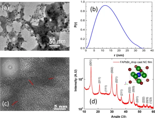
The as-prepared perovskite NCs are primarily polycrystalline having broad size distribution. Figure 2(a) shows the transmission electron microscopy (TEM) image of FAPbBr3 NCs. The FAPbBr3 NCs have an average
size of 10–15 nm. We have also measured the particle size distribution via small angle x-ray scattering technique and the as synthesized FAPbBr3 NCs have particle distribution from 1–30 nm with an average size of 12–14 nm
shown in Fig. 2(b). The average size obtained from SAXS are consistent with the TEM measurements. Further information as to how to formulate the particle size from SAXS is described in Supplementary Information. We can also resolve the crystalline lattice planes of these FAPbBr3 NCs in the high resolution transmission electron
microscopy (HR-TEM) image shown in (Fig. 2(c)) with its fast Fourier transformation (FFT) image shown in the inset of Fig. 2(c). The TEM measurements confirm high degree of crystallinity in these FAPbBr3 NCs. X-ray
diffraction (XRD) pattern for drop cast FAPbBr3 NCs is recorded at room temperature and the XRD spectra is
shown in Fig. 2(d).
The XRD data clearly shows that the NCs are highly polycrystalline. The XRD patterns are indexed to the cubic phase of FAPbBr3 with a unit cell of 6.006 Å with Pm-3 m space group, similar to that of bulk FAPbBr3
perovskite17,51. The detailed indexing is shown in Table ST1 of supplementary info. The inter-planar distance of
~3 Å from the HR-TEM image correspond to the 002 plane of crystal orientation in XRD analysis. According to temperature dependent PL studies performed for MAPbBr3 bulk films, it is reported that at room temperature
the MAPbBr3 bulk film is in tetragonal phase52, there is phase transition from tetragonal to cubic phase at 320 K.
Due to similarities in MAPbBr3 and FAPbBr3 structures, we propose that the FAPbBr3 to be in tetragonal phase at
room temperature. However, the XRD measurements and indexing performed at room temperature indicate the FAPbBr3 NC film to be in cubic phase as the XRD peaks are indexed to cubic phase (tetragonal indexing for XRD
measurements resulted in lattice constants a and b to be very similar). From temperature dependent PL studies performed on MAPbBr3 and assuming the phase transitions for MAPbBr3 and FAPbBr3 to be similar, we believe
that it is difficult to differentiate between these two phases.
Figure 2. (a) Transmission electron microscopy (TEM) image of FAPbBr3 NCs. The black dots correspond
to FAPbBr3 NCs having an average size of 10–15 nm. (b) Particle size distributions measured via small angle
x-ray scattering technique (SAXS) the as synthesized FAPbBr3 NCs with an average size of 12–14 nm.
(c) The high-resolution transmission electron microscopy (HR-TEM) of the FAPbBr3 NCs with its fast Fourier
transformation (FFT) image shown in the inset. (d) X-ray diffraction (XRD) patterns for drop cast FAPbBr3
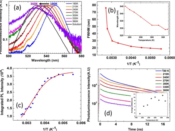
Temperature dependent exciton dynamics studies are performed to extract exciton binding energy and to understand PL dynamics as a function of temperature for FAPbBr3 NC thin films. The exciton binding energy is
directly related to the absorption and emission of an optoelectronic material.
Figure 3(a) shows normalized PL spectra for the temperature range from 180–360 K for FAPbBr3 NC thin
film under an excitation pump fluence of 1.2 μ J cm−2. We restrict our temperature dependent studies to 180 K
as the low temperature limit due to experimental constraints and we believe below 180 K the low temperature PL exciton dynamics to be similar to the MAPbBr3 thin films reported earlier52. The FWHM increases as the
temperature increases as shown in Fig. 3(b) and this is attributed to increased phonon interactions and phonon scattering53,54. The thin film PL at 180 K is narrower with FWHM of 18.6 nm, while at 360 K the FWHM of the PL
is 46.9 nm. There is red shift in PL peak position with lowering temperature consistent with FAPbBr3 bulk thin
films and other lead halide perovskites49,53,54, the PL peak is at ~530 nm at room temperature and the PL peak
shifts to ~545 nm at 180 K as shown in the inset of Fig. 3(b). This is attributed to lattice strain53, contraction of the
lattice and reorientation of crystallites in the lattice54. The integrated PL emission intensity (area under the PL
peak at different temperatures) versus the inverse of temperature for FAPbBr3 NCs and the Arrhenius fits in the
temperature range 180–360 K is shown in Fig. 3(c).
We also observe significant reduction in the absolute PL intensity with increase in temperature as shown in Figure S1 of supplementary info. The nonradioactive recombination is thermally activated in FAPbBr3 and is
increasing with the temperature. We can extract exciton binding energy of these nanocrystals by fitting the curve with following equation55,
= + − I t I Ae ( ) 1 (1) 0 Eb kBT
where I0 is the emission intensity extrapolated at 0 K, Eb is the exciton binding energy, and kB is the Boltzmann
constant.
We find that the exciton binding energy of FAPbBr3 NCs we synthesized is roughly 170 meV (Fig. 3(c))
which is much higher than the reported exciton binding energies of the bulk thin films49. We have measured
the time-resolved PL spectra for FAPbBr3 NCs in thin film and in solution as shown in Fig. 3(d) for temperature
range 180–360 K. The PL decay transients can be fitted with the bi-exponential of the form23,
Figure 3. (a) The normalized PL emission spectra under a pump fluence of 1.2 μ J cm−2 at temperatures ranging
from 180–360 K. The PL spectra are normalized at their maximum intensity. (b) The change in FWHM is shown as a function of inverse temperature and in the inset the shift in the PL emission peak is shown as a function of temperature. (c) The integrated PL intensity as a function of inverse temperature and the Arrhenius fit (solid line) for temperature range 180–360 K (d) The TRPL intensity and the fit along with the average lifetime (inset) is shown for temperature range of 180–360 K.
www.nature.com/scientificreports/
τ τ = − + − A t( ) A exp t A exp t (2) 1 1 2 2For both thin film and solution, we observe bi-exponential decay resulting in two time constants one with the shorter lifetime, which we attribute to NCs whose recombination is strongly mediated by surface impurities and traps and the longer lifetime due to intrinsic band edge emission. The relative contribution of these two terms to the PL emission in solution shows that the fast component has only 20% contribution of the total PL emission and the faster lifetime component is ~5 ns. The rest 80% contribution of the PL emission is due to band edge emission and the corresponding slower component lifetime is ~69 ns. The TRPL for NCs in solution is shown in supple-mentary info Figure S3. For NC thin films, the faster component proportion roughly doubles in comparison to the solution sample from 20% to 32% at room temperature. The surface of the NCs is exposed in case of thin films and the surface trap density is much higher than in the case of the solution. The shorter lifetime τ 1 is decreasing
with increasing temperatures due to possible non-radiative recombination. The slower component proportion is reduced from 80% in solution to ~70% in NC thin films at room temperature. The longer component τ 2 increases
with increasing temperature a similar to the trend that is observed in CdSe nano sheets, which is attributed to the giant oscillator strength (GOST) effect in low dimensions56. Although the average lifetime increases as a
function of increasing temperature as shown in Table 1 and the inset of Fig. 3(d), the absolute PL signal intensity significantly decreases (shown in Figure S1 of supplementary info). This implies the PL quantum yield decreases as a function of increasing temperature, which is consistent with previous report in perovskite bulk films57. The
average lifetime of FAPbBr3 NCs film is much shorter in comparison to the solution sample, at room temperature
NC thin film has average lifetime of 10 ns with PLQE roughly 25%. The solution of FAPbBr3 in toluene on the
other hand has much larger average lifetime of 55 ns and also much higher PLQE of 55–65%.
We can estimate the exciton Bohr radius for these FAPbBr3 NC system from the following equation,
ε µ = ħ a e (3) b 2 2
where ε is the static dielectric constant, ħ is the Planck’s constant 1.05 ∗ 10−34 Js, μ is the reduced exciton effective
mass (the bulk value 0.13 m058) and e is unit charge of electron 1.6 ∗ 10−19 Js coulomb. The perovskite NC film is not
dense in comparison to bulk perovskite film and hence the static dielectric constant value will be lower in compar-ison to bulk. The estimated Bohr radius is dependent on the value of the static dielectric constant. The exciton is also screened by phonons and random distribution of polar organic cation hence the value of ε is not easy to esti-mate in these films. With ε of ~20 (for MAPbI3 bulk films the static ε is reported to be in the range of 35–7059), we
estimate the Bohr exciton radius to be 8 nm much larger than the lattice constant. We do not observe the strong quantum confinement effect in these nanocrystals as a function of size due to their relatively larger size. This observation is supported by the PL emission measurements of supernatant (having nanocrystals of smaller size) and the precipitate (having nanocrystals of much larger size compared to supernatant), their emission maxima does not have strong shift as shown in supporting info Figure S2.
We fabricate the Pe-LED device with these FAPbBr3 NCs. The device structure and the flat band energy level
diagram is shown in Fig. 4(a). The Pe-LED device with FAPbBr3 perovskite NCs consists of 40 nm thick
poly(eth-ylenedioxythiophene):polystyrene (PEDOT:PSS) as hole transport/injection layer, FAPbBr3 NC layer and ~50 nm
of B3PYMPM or TPBi as an electron transport layer with CsCO3 (5 nm)/Al(100 nm) cathode layer. To observe
any discontinuity in perovskite film and to see the thin film morphology, we perform the cross-sectional TEM imaging of the complete Pe-LED device. Figure S5 of Supplementary Information shows a cross-sectional TEM image of the Pe-LED device, with ITO and aluminum layers clearly identified. The HTL, perovskite EML and ETL in the device stack are not resolved as there is insufficient scattering contrast between them as there is dominant carbon content in all these films. The energy levels for the FAPbBr3 NC layer are derived from UPS measurement
shown in Figure S4 (Supplementary Information) and the energy level values for indium tin oxide (ITO) act-ing as semi-transparent electrode, PEDOT:PSS hole injection/transport layer (HIL/HTL), B3PYMPM and TPBi
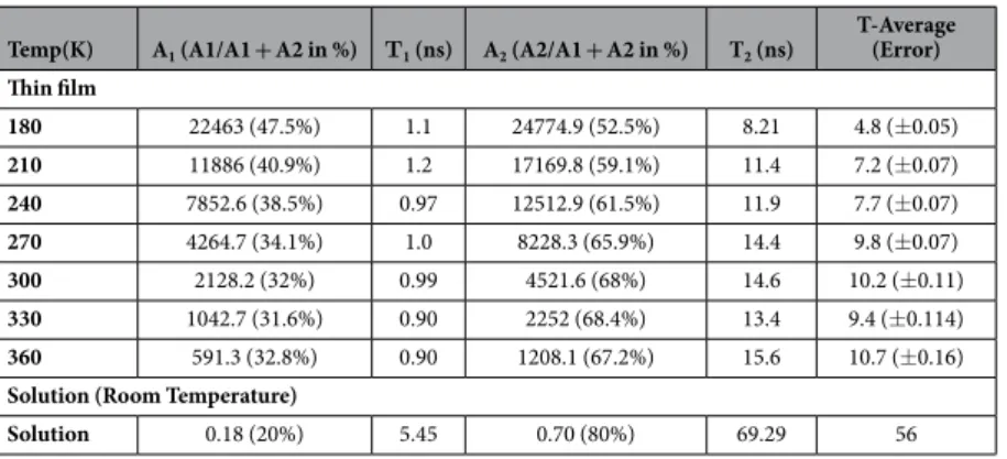
Temp(K) A1 (A1/A1 + A2 in %) Τ1 (ns) A2 (A2/A1 + A2 in %) T2 (ns)
T-Average (Error) Thin film 180 22463 (47.5%) 1.1 24774.9 (52.5%) 8.21 4.8 (± 0.05) 210 11886 (40.9%) 1.2 17169.8 (59.1%) 11.4 7.2 (± 0.07) 240 7852.6 (38.5%) 0.97 12512.9 (61.5%) 11.9 7.7 (± 0.07) 270 4264.7 (34.1%) 1.0 8228.3 (65.9%) 14.4 9.8 (± 0.07) 300 2128.2 (32%) 0.99 4521.6 (68%) 14.6 10.2 (± 0.11) 330 1042.7 (31.6%) 0.90 2252 (68.4%) 13.4 9.4 (± 0.114) 360 591.3 (32.8%) 0.90 1208.1 (67.2%) 15.6 10.7 (± 0.16) Solution (Room Temperature)
Solution 0.18 (20%) 5.45 0.70 (80%) 69.29 56
Table 1. Summarizes the FAPbBr3 NC film and solution PL decay lifetimes and amplitude values as a function of temperature.
electron transport layer (ETL) are taken from refs 20 and 60. The normalized EL spectra of the perovskite LED device with TPBi and B3PYMPM as ETL, the normalized PL spectrum of FAPbBr3 NC film is shown in Fig. 4(b).
The EL emission is due to radiative recombination of excitons in FAPbBr3 NCs as the EL and PL spectra overlap
and the small shift in the EL spectra for Pe-LED with TPBi layer is due to optical detuning of cavity from emission maxima. This is evident from the change in the EL spectra with the change in ETL.
The refractive index of B3PYMPM and TPBi are slightly different, hence for the device with the same thick-ness of ETL while keeping the other layers/thickthick-nesses same results in an EL emission which is slightly red shifted. The FWHM of the EL spectrum is slightly broader in comparison to the PL spectra of neat FAPbBr3 thin
film. The FAPbBr3 PL emission has a FWHM of 22.5 nm with ~λ max of 530 nm. The EL emission spectra of the
Pe-LED device with TPBi as ETL has a FWHM of 21.2 nm with ~λ max of 533.4 nm while the Pe-LED device with
B3PYMPM as ETL has a FWHM of 23.5 nm with ~λ max of 530.7 nm. The current density-voltage-luminance
curve for Pe-LED devices with TPBi and B3PYMPM as ETL layers is shown in Fig. 4(c). The turn-on voltages (corresponds to luminance of 1 cd m−2) are 2.8 and 2.3 V for Pe-LED devices with TPBi and B3PYMPM ETLs.
The luminance-voltage plot is similar for both ETLs. Initially, the luminance increases as a function of increas-ing voltage until 465 cd m−2 at 4.4 V (for TPBi ETL) and 2714 cd m−2 at 3.8 V (for B3PYMPM ETL) beyond the
luminance maximum the increase in voltage results in decrease of luminance. The B3PYMPM ETL has superior electron mobility and better energetic alignment61, hence higher current densities in the Pe-LED device therefore
resulting in higher luminance. The deeper HOMO of the B3PYMPM also helps in tighter exciton confinement, hence the device with B3PYMPM has a lower onset voltage. The Pe-LED device with TPBi as ETL has lower cur-rent density, lower luminance and superior efficiency values. The luminous and luminous power efficiency as a function of the luminance is shown in Fig. 4(d).
We achieve maximum luminous efficiency of 6.4 cd A−1 and a maximum luminous power efficiency of
5.6 lmW−1 for the Pe-LED device with TPBi as ETL. For the Pe-LED device with B3PYMPM as ETL, we achieve
a maximum current efficiency of 5.4 cd A−1 and a maximum luminous efficiency of 5.7 lmW−1. There is a severe
roll off in luminance and device efficiency beyond 3.8 V (98 mA/cm2) or the maximum luminance of 2714 cd/m2
for the device with B3PYMPM as ETL and 4.8 V (16 mA/cm2) or the maximum luminance of 434 cd/m2 for the
device with TPBi as ETL. The Pe-LED device with both B3PYMPM and TPBi has a charge imbalance evident from the increase in efficiency until there is charge balance in the device. The sudden roll-off thereafter is severe
Figure 4. (a) The device structure for the Pe-LED device and the corresponding schematic energy level
diagram for the materials. (b) EL spectra for Pe-LED device with B3PYMPM (green line) and TPBi (blue line) as ETL are shown in Fig. 4 recorded at 0.5 mA/cm2. The PL spectrum of FAPbBr
3 (red line is also shown
for reference). (c) Current density/Luminance vs Voltage (J-V-L) characteristics for Pe-LED device with B3PYMPM (green line circles) and TPBi (blue line stars). (d) Luminous efficiency (cd/A) vs luminance (cd/m2) and Luminous power efficiency (lm/W) vs luminance (cd/m2) characteristics for Pe-LED device with
B3PYMPM (green line circles) and TPBi (blue line stars). The filled symbols correspond to luminous efficacy cd/A and open symbols correspond to lm/W.
www.nature.com/scientificreports/
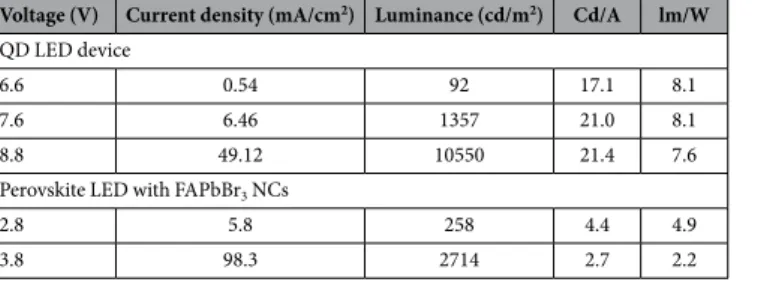
and this roll off is similar in Pe-LED devices with different ETLs. The difference in the magnitude of the current density values (higher current density with B3PYMPM and lower current density with TPBi) does not have an influence on the quenching and efficiency roll off. The PLQE measured as a function of input laser power shown in Supplementary info Figure S7, for perovskite thin film has roughly same value. Implying the exciton quenching due to higher exciton density is less significant in Pe-LED devices. Hence, the charge injection seems to result in degradation of perovskite material ultimately causing the efficiency roll off. We compare typical current density, luminance and efficiency values for a quantum dot light emitting device (QD-LED) with similar device architec-ture except the difference in emission layer. The quantum dots have similar PLQE values ranging from 65–70%. The device performance values for both QD-LED device and the Pe-LED device are tabulated in Table 2 at 100, 1000 and 10000 cd/m2. The QD-LED device shows much higher luminance and efficiency values at lower current
density in comparison to Pe-LED device. Hence, we believe better material engineering is essential to achieve higher efficiency in perovskite NC LED devices, our results clearly demonstrate that with the better perovskite material having lesser PL quenching at room temperature it should be possible to achieve much higher efficiency in Pe-LED devices.
Conclusions
In conclusion, we have demonstrated highly reproducible room temperature synthesis of device grade high qual-ity formamidinium lead bromide (FAPbBr3) colloidal nanocrystals (NC). The perovskite NC synthesized have
high PLQE of 55–65% and have very narrow FWHM of ~20 nm suitable for display applications with high color purity. We also demonstrate high brightness perovskite light emitting device (Pe-LED) with these FAPbBr3
per-ovskite NC thin film using TPBi and B3PYMPM as electron transport layers (ETL). The Pe-LED device with TPBi as ETL has bright electroluminescence of up to 2714 cd/m2, while the Pe-LED device with B3PYMPM as ETL as
higher peak luminous efficiency of 6.4 cd/A and peak luminous power efficiency of 5.7 lm/W. To our knowledge this is the first report on high brightness light emitting device based on FAPbBr3 nanocrystals in literature. Our
studies indicate that the roll off in efficiency and the low performance in perovskite NC LED devices is attributed to the lattice changes due to charge injection and material degradation of the perovskite film. Hence, we believe better material engineering is essential to achieve higher efficiency in perovskite NC LED devices, our results clearly demonstrate that with the better perovskite material having lesser PL quenching at room temperature it should be possible to achieve much higher efficiency in Pe-LED devices.
Methods
Synthesis of (CH(NH
2)
2PbBr
3or FAPbBr
3NCs.
0.1 mmol lead(II) bromide from Sigma Aldrich (36.7 mg) and 0.1 mmol formamidinium bromide from Dyesol (25.6 mg) is dissolved in 0.5 mL of DMF which we name it as precursor solution. In a beaker 5 mL toluene, 10 μ L octylamine, 0.5 mL of oleic acid and 2 mL of butanol are added sequentially in that order and mixed on a magnetic stirrer at 800 rpm at room temperature. To this solution 150 μ L of the precursor solution is added dropwise. The NCs are formed instantaneously, it is confirmed by color change – the transparent toluene solution turns bright yellowish green in color. Purification stage consists of 2 centrifuge steps. First centrifugation is performed at 7500 rpm for 5 minutes, this will remove all the unreactive materials in the supernatant and the supernatant is discarded and the bottom precipitate is used for further purification. 2 mL toluene is added for another centrifugation at 7500 rpm for 5 min. This time the supernatant is transferred to vial for further use in device fabrication.Perovskite film characterization.
XRD data are collected on a Bruker Advance D8 X-ray diffractometer, using Cu-Kα radiation, at a scanning rate of 0.01° per step. X-ray photoelectron spectroscopy (XPS) and ultravio-let photoelectron spectroscopy (UPS) measurements are performed on the drop cast NC samples in UHV system. The XPS source is monochromatic Al Kα with photon energy at 1486.7 eV. The UPS source is from a helium dis-charge lamp (hν = 21.2 eV). The emitted photoelectrons are measured via an electron analyser (Omicron EA125). Small Angle X-ray Scattering (SAXS) experiments are performed using a SAXSess camera (Anton Paar, Graz, Austria) with a Cu anode X-ray source (PANalytical, PW3830) operating at 40 kV and 50 mA. Using a Goebel mirror and a collimation block the divergent polychromatic X-ray beam is collimated to a line-shaped beam of Cu Kα radiation (l = 0.154 nm). The perovskite nanocrystals are dispersed in toluene and the solution is held in a quartz capillary holder. The experiment is performed at room temperature and the scattering pattern is col-lected on an imaging plate. Raw data processing (Integration and background subtraction) is performed using SAXSQuant software from Anton-Paar. The SAXS data is evaluated using an indirect Fourier transform (GIFT software from Anton-Paar) to obtain the pair distance distribution function (PDDF) p(r), which can be used toVoltage (V) Current density (mA/cm2) Luminance (cd/m2) Cd/A lm/W
QD LED device
6.6 0.54 92 17.1 8.1
7.6 6.46 1357 21.0 8.1
8.8 49.12 10550 21.4 7.6
Perovskite LED with FAPbBr3 NCs
2.8 5.8 258 4.4 4.9
3.8 98.3 2714 2.7 2.2
determine the overall size and shape of the dispersed perovskite nanocrystals. TEM images are recorded on JEOL 2100F advanced field emission microscope operating at 200 kV accelerating voltage. The solution absorption is measured using Shimadzu spectrophotometer. The PL spectra are recorded with RF-5301PC fluorescence spec-trometer (SHIMADZU). PLQE is measured using an integrated sphere and a fiber specspec-trometer (Ocean Optics USB 4000). The excitation source is 405 nm blue laser (Cobolt MLDTM). Temperature dependent steady state
photoluminescence (PL) and time-resolved PL (TRPL) are performed with a Coherent LibraTM femtosecond
regenerative amplifier (1 kHz, ~50 fs) with frequency doubled 400 nm pulses at a pump fluence of 1.2 μ J cm−2
per pulse as the excitation source. The PL emission is collected in a conventional backscattering geometry and detected by a charge-coupled device array (Princeton Instruments, PixisTM) coupled to a monochromator (Acton,
Spectra ProTM). The temporal evolution of the PL is resolved by an Optronis OptoscopeTM streak camera system.
Device fabrication and characterization.
ITO coated glass substrates with 10 ohm/square sheet resistance are purchased from Xiamen Weihua solar Co Ltd China. The substrates are sequentially washed with acetone, soap solution, ethanol and deionized water, followed by plasma treatment for 10 min at 100 W before use. The poly(3,4-ethylenedioxythiophene):poly(styrene-sulfonate) (PEDOT:PSS) Clevios Al 4043 Heraus GmbH solution is spin coated on the ITO film at 4000 rpm for 60 seconds, then it is annealed at 150 °C for 15 min. Then FAPbBr3 colloidal nanocrystals dispersed in toluene is spin-coated on the PEDOT:PSS film,followed by thermal annealing at 50 °C for 1 min. The substrates are then transferred to high vacuum ther-mal evaporator chamber, where 4,6-Bis(3,5-di(pyridin-3-yl)phenyl)-2-methylpyrimidine (B3PYMPM) or 2,2′ ,2″ -(1,3,5-Benzinetriyl)-tris(1-phenyl-1-H-benzimidazole) TPBi (40 nm), Caesium carbonate (CsCO3)
(5 nm) and Aluminium (Al) (80 nm) are sequentially thermally deposited. The active area of the devices fabri-cated in this work are 3 mm2. Devices are encapsulated before characterization.
The current–voltage–luminance characteristics is recorded via computer controlled source measure unit (Yokogawa GS610) and Konica Minolta LS-110 Luminance Meter. For measuring EQE of the LED device, Yokogawa GS610 source measure unit linked to a calibrated silicon photodiode is used to measure the current– voltage–luminance characteristics and the electroluminescence spectra of the LED device are recorded via a spec-trophotometer PR-655 (Photo Research, Inc.). The lifetime test is performed via photodiode placed on top of the LED device and the photodiode is controlled via a source measure unit in a constant current mode.
References
1. D’Innocenzo, V. et al. Excitons versus free charges in organo-lead tri-halide perovskites. Nat Commun 5, 3586, doi: 10.1038/ ncomms4586 (2014).
2. Zheng, F., Saldana-Greco, D., Liu, S. & Rappe, A. M. Material Innovation in Advancing Organometal Halide Perovskite Functionality. J Phys Chem Lett 6, 4862–4872, doi: 10.1021/acs.jpclett.5b01830 (2015).
3. Nedelcu, G. et al. Fast Anion-Exchange in Highly Luminescent Nanocrystals of Cesium Lead Halide Perovskites (CsPbX3, X = Cl, Br, I). Nano Lett 15, 5635–5640, doi: 10.1021/acs.nanolett.5b02404 (2015).
4. Saba, M., Quochi, F., Mura, A. & Bongiovanni, G. Excited State Properties of Hybrid Perovskites. Acc Chem Res 49, 166–173, doi: 10.1021/acs.accounts.5b00445 (2016).
5. Even, J. et al. Solid-State Physics Perspective on Hybrid Perovskite Semiconductors. The Journal of Physical Chemistry C 119, 10161–10177, doi: 10.1021/acs.jpcc.5b00695 (2015).
6. Stranks, S. D. & Snaith, H. J. Metal-halide perovskites for photovoltaic and light-emitting devices. Nat Nanotechnol 10, 391–402, doi: 10.1038/nnano.2015.90 (2015).
7. Berry, J. et al. Hybrid Organic-Inorganic Perovskites (HOIPs): Opportunities and Challenges. Adv Mater 27, 5102–5112, doi: 10.1002/adma.201502294 (2015).
8. Saparov, B. & Mitzi, D. B. Organic-Inorganic Perovskites: Structural Versatility for Functional Materials Design. Chem Rev 116, 4558–4596, doi: 10.1021/acs.chemrev.5b00715 (2016).
9. Gratzel, M. The light and shade of perovskite solar cells. Nat Mater 13, 838–842, doi: 10.1038/nmat4065 (2014).
10. Liu, M., Johnston, M. B. & Snaith, H. J. Efficient planar heterojunction perovskite solar cells by vapour deposition. Nature 501, 395–398, doi: 10.1038/nature12509 (2013).
11. Snaith, H. J. Perovskites: The Emergence of a New Era for Low-Cost, High-Efficiency Solar Cells. The Journal of Physical Chemistry
Letters 4, 3623–3630, doi: 10.1021/jz4020162 (2013).
12. Green, M. A., Ho-Baillie, A. & Snaith, H. J. The emergence of perovskite solar cells. Nature Photonics 8, 506–514, doi: 10.1038/ nphoton.2014.134 (2014).
13. Lee, M. M., Teuscher, J., Miyasaka, T., Murakami, T. N. & Snaith, H. J. Efficient Hybrid Solar Cells Based on Meso-Superstructured Organometal Halide Perovskites. Science 338, 643–647 (2012).
14. Jeon, N. J. et al. Compositional engineering of perovskite materials for high-performance solar cells. Nature 517, 476–480, doi: 10.1038/nature14133 (2015).
15. Yang, W. S. et al. High-performance photovoltaic perovskite layers fabricated through intramolecular exchange. Science 348, 1234–1237, doi: 10.1126/science.aaa9272 (2015).
16. Han, Q. et al. Single Crystal Formamidinium Lead Iodide (FAPbI3): Insight into the Structural, Optical, and Electrical Properties.
Adv Mater 28, 2253–2258, doi: 10.1002/adma.201505002 (2016).
17. Eperon, G. E. et al. Formamidinium lead trihalide: a broadly tunable perovskite for efficient planar heterojunction solar cells. Energy
& Environmental Science 7, 982, doi: 10.1039/c3ee43822h (2014).
18. D’Innocenzo, V., Srimath Kandada, A. R., De Bastiani, M., Gandini, M. & Petrozza, A. Tuning the light emission properties by band gap engineering in hybrid lead halide perovskite. J Am Chem Soc 136, 17730–17733, doi: 10.1021/ja511198f (2014).
19. Huang, H. et al. Emulsion Synthesis of Size-Tunable CH3NH3PbBr3 Quantum Dots: An Alternative Route toward Efficient Light-Emitting Diodes. ACS Appl Mater Interfaces 7, 28128–28133, doi: 10.1021/acsami.5b10373 (2015).
20. Zhang, X. et al. Enhancing the Brightness of Cesium Lead Halide Perovskite Nanocrystal Based Green Light-Emitting Devices through the Interface Engineering with Perfluorinated Ionomer. Nano Lett 16, 1415–1420, doi: 10.1021/acs.nanolett.5b04959 (2016).
21. Wong, A. B. et al. Growth and Anion Exchange Conversion of CH3NH3PbX3 Nanorod Arrays for Light-Emitting Diodes. Nano Lett 15, 5519–5524, doi: 10.1021/acs.nanolett.5b02082 (2015).
22. Zhang, F. et al. Brightly Luminescent and Color-Tunable Colloidal CH3NH3PbX3 (X = Br, I, Cl) Quantum Dots: Potential Alternatives for Display Technology. Acs Nano 9, 4533–4542 (2015).
www.nature.com/scientificreports/
23. Li, X. et al. CsPbX3Quantum Dots for Lighting and Displays: Room-Temperature Synthesis, Photoluminescence Superiorities, Underlying Origins and White Light-Emitting Diodes. Advanced Functional Materials, n/a-n/a, doi: 10.1002/adfm.201600109 (2016).
24. Ling, Y. et al. Bright Light-Emitting Diodes Based on Organometal Halide Perovskite Nanoplatelets. Adv Mater 28, 305–311, doi: 10.1002/adma.201503954 (2016).
25. Tan, Z. K. et al. Bright light-emitting diodes based on organometal halide perovskite. Nat Nanotechnol 9, 687–692, doi: 10.1038/ nnano.2014.149 (2014).
26. Li, G. et al. Efficient light-emitting diodes based on nanocrystalline perovskite in a dielectric polymer matrix. Nano Lett 15, 2640–2644, doi: 10.1021/acs.nanolett.5b00235 (2015).
27. Sadhanala, A. et al. Electroluminescence from Organometallic Lead Halide Perovskite Conjugated Polymer Diodes. Advanced
Electronic Materials 1 (2015).
28. Wang, J. et al. Interfacial Control Toward Efficient and Low Voltage Perovskite Light Emitting Diodes. Advanced Materials 27, 2311–2316 (2015).
29. Hoye, R. L. et al. Enhanced Performance in Fluorene Free Organometal Halide Perovskite Light Emitting Diodes using Tunable, Low Electron Affinity Oxide Electron Injectors. Advanced Materials 27, 1414–1419 (2015).
30. Shi, Z. et al. High-performance planar green light-emitting diodes based on PEDOT:PSS/CH3NH3PbBr3/ZnO sandwiched structure. Nanoscale, doi: 10.1039/c6nr00818f (2016).
31. Kim, Y. H. et al. Multicolored organic/inorganic hybrid perovskite light-emitting diodes. Adv Mater 27, 1248–1254, doi: 10.1002/ adma.201403751 (2015).
32. Brenner, T. M., Egger, D. A., Kronik, L., Hodes, G. & Cahen, D. Hybrid organic—inorganic perovskites: low-cost semiconductors with intriguing charge-transport properties. Nature Reviews Materials 1, 15007, doi: 10.1038/natrevmats.2015.7 (2016).
33. Akkerman, Q. A. et al. Tuning the Optical Properties of Cesium Lead Halide Perovskite Nanocrystals by Anion Exchange Reactions.
J Am Chem Soc 137, 10276–10281, doi: 10.1021/jacs.5b05602 (2015).
34. Era, M., Morimoto, S., Tsutsui, T. & Saito, S. Organic-inorganic heterostructure electroluminescent device using a layered perovskite semiconductor (C6H5C2H4NH3)2PbI4. Applied Physics Letters 65, 676, doi: 10.1063/1.112265 (1994).
35. Hattori, T., Taira, T., Era, M., Tsutsui, T. & Saito, S. Highly efficient electroluminescence from a heterostructure device combined with emissive layered-perovskite and an electron-transporting organic compound. Chem Phys Lett 254, 103–108 (1996). 36. Chondroudis, K. & Mitzi, D. B. Electroluminescence from an organic-inorganic perovskite incorporating a quaterthiophene dye
within lead halide perovskite layers. Chemistry of Materials 11, 3028–3030, doi: DOI 10.1021/cm990561t (1999).
37. Cho, H. C. et al. Overcoming the electroluminescence efficiency limitations of perovskite light-emitting diodes. Science 350, 1222–1225 (2015).
38. Xing, G. et al. Low-temperature solution-processed wavelength-tunable perovskites for lasing. Nat Mater 13, 476–480, doi: 10.1038/ nmat3911 (2014).
39. Zhu, H. et al. Lead halide perovskite nanowire lasers with low lasing thresholds and high quality factors. Nat Mater 14, 636–642, doi: 10.1038/nmat4271 (2015).
40. Fu, Y. et al. Nanowire Lasers of Formamidinium Lead Halide Perovskites and Their Stabilized Alloys with Improved Stability. Nano
Lett 16, 1000–1008, doi: 10.1021/acs.nanolett.5b04053 (2016).
41. Chin, X. Y., Cortecchia, D., Yin, J., Bruno, A. & Soci, C. Lead iodide perovskite light-emitting field-effect transistor. Nat Commun 6, 7383, doi: 10.1038/ncomms8383 (2015).
42. Gonzalez-Carrero, S., Galian, R. E. & Perez-Prieto, J. Organic-inorganic and all-inorganic lead halide nanoparticles [Invited]. Opt
Express 24, A285–A301, doi: 10.1364/OE.24.00A285 (2016).
43. Protesescu, L. et al. Nanocrystals of Cesium Lead Halide Perovskites (CsPbX(3), X = Cl, Br, and I): Novel Optoelectronic Materials Showing Bright Emission with Wide Color Gamut. Nano Lett 15, 3692–3696, doi: 10.1021/nl5048779 (2015).
44. Schmidt, L. C. et al. Nontemplate synthesis of CH3NH3PbBr3 perovskite nanoparticles. J Am Chem Soc 136, 850–853, doi: 10.1021/ ja4109209 (2014).
45. Kim, J. Y., Voznyy, O., Zhitomirsky, D. & Sargent, E. H. 25th anniversary article: Colloidal quantum dot materials and devices: a quarter-century of advances. Adv Mater 25, 4986–5010, doi: 10.1002/adma.201301947 (2013).
46. Shirasaki, Y., Supran, G. J., Bawendi, M. G. & Bulović, V. Emergence of colloidal quantum-dot light-emitting technologies. Nature
Photonics 7, 13–23, doi: 10.1038/nphoton.2012.328 (2012).
47. Song, J. et al. Quantum Dot Light-Emitting Diodes Based on Inorganic Perovskite Cesium Lead Halides (CsPbX3 ). Adv Mater 27, 7162–7167, doi: 10.1002/adma.201502567 (2015).
48. Aygüler, M. F. et al. Light-Emitting Electrochemical Cells Based on Hybrid Lead Halide Perovskite Nanoparticles. The Journal of
Physical Chemistry C 119, 12047–12054, doi: 10.1021/acs.jpcc.5b02959 (2015).
49. Fang, H.-H. et al. Photoexcitation dynamics in solution-processed formamidinium lead iodide perovskite thin films for solar cell applications. Light: Science & Applications 5, e16056, doi: 10.1038/lsa.2016.56 (2015).
50. Arora, N. et al. Photovoltaic and Amplified Spontaneous Emission Studies of High-Quality Formamidinium Lead Bromide Perovskite Films. Advanced Functional Materials, n/a-n/a, doi: 10.1002/adfm.201504977 (2016).
51. Hanusch, F. C. et al. Efficient Planar Heterojunction Perovskite Solar Cells Based on Formamidinium Lead Bromide. J Phys Chem
Lett 5, 2791–2795, doi: 10.1021/jz501237m (2014).
52. Milot, R. L., Eperon, G. E., Snaith, H. J., Johnston, M. B. & Herz, L. M. Temperature-Dependent Charge-Carrier Dynamics in CH3NH3PbI3Perovskite Thin Films. Advanced Functional Materials 25, 6218–6227, doi: 10.1002/adfm.201502340 (2015). 53. Huang, L.-y. & Lambrecht, W. R. L. Electronic band structure, phonons, and exciton binding energies of halide perovskites CsSnCl3,
CsSnBr3, and CsSnI3. Phys Rev B 88, doi: 10.1103/PhysRevB.88.165203 (2013).
54. Yu, C. L. et al. Temperature dependence of the band gap of perovskite semiconductor compound CsSnI3. Journal of Applied Physics
110 (2011).
55. Wu, K. et al. Temperature-dependent excitonic photoluminescence of hybrid organometal halide perovskite films. Phys Chem Chem
Phys 16, 22476–22481, doi: 10.1039/c4cp03573a (2014).
56. Achtstein, A. W. et al. Electronic structure and exciton-phonon interaction in two-dimensional colloidal CdSe nanosheets. Nano
Lett 12, 3151–3157, doi: 10.1021/nl301071n (2012).
57. Stranks, S. D. et al. Recombination Kinetics in Organic-Inorganic Perovskites: Excitons, Free Charge, and Subgap States. Physical
Review Applied 2, doi: 10.1103/PhysRevApplied.2.034007 (2014).
58. Tanaka, K. et al. Comparative study on the excitons in lead-halide-based perovskite-type crystals CH3NH3PbBr3 CH3NH3PbI3. Solid
State Commun 127, 619–623, doi: 10.1016/s0038-1098(03)00566-0 (2003).
59. Lin, Q., Armin, A., Nagiri, R. C. R., Burn, P. L. & Meredith, P. Electro-optics of perovskite solar cells. Nature Photonics 9, 106–112, doi: 10.1038/nphoton.2014.284 (2014).
60. Perumal, A. et al. High Efficiency, Solution Processed, Multilayer Phosphorescent Organic Light Emitting Diodes with a Copper Thiocyanate Hole Injection/Hole Transport Layer. Advanced Materials 27, 93–100 (2015).
61. Sasabe, H. et al. 2-Phenylpyrimidine skeleton-based electron-transport materials for extremely efficient green organic light-emitting devices. Chem Commun (Camb), 5821–5823, doi: 10.1039/b812270a (2008).
Acknowledgements
This research is supported by the National Research Foundation, Prime Minister’s Office, Singapore under its competitive Research Programme (CRP Award No. NRF-CRP14-2014-03). H.V.D acknowledges the financial support from NRF Investigatorship grant NRF-NRFI2016-08. T.C.S. acknowledges the financial support from NTU start-up grant M4080514; the Ministry of Education AcRF Tier 1 grant RG101/15, and Tier 2 grants MOE2013-T2-1-081 and MOE2014-T2-1-044.
Author Contributions
A.P. and H.V.D. conceived the idea and designed the experiment. A.P. synthesized and prepared the samples for all characterizations, also A.P. fabricated and tested the LED devices which was supervised by H.V.D. S.S. assisted in LED device fabrication. M.L.J. and Y.K.T.E. carried out temperature dependent time resolved measurements and was supervised by T.C.S. Q.L. performed TEM cross-section and FIB measurements, was supervised by C.L.G. S.C. measured U.P.S. and X.P.S. scans. A.P. and H.V.D. together with all authors carried out data analysis. The manuscript is prepared through contributions of all authors. All authors have given approval to the final version of the manuscript.
Additional Information
Supplementary information accompanies this paper at http://www.nature.com/srep Competing financial interests: The authors declare no competing financial interests.
How to cite this article: Perumal, A. et al. High brightness formamidinium lead bromide perovskite
nanocrystal light emitting devices. Sci. Rep. 6, 36733; doi: 10.1038/srep36733 (2016).
Publisher's note: Springer Nature remains neutral with regard to jurisdictional claims in published maps and
institutional affiliations.
This work is licensed under a Creative Commons Attribution 4.0 International License. The images or other third party material in this article are included in the article’s Creative Commons license, unless indicated otherwise in the credit line; if the material is not included under the Creative Commons license, users will need to obtain permission from the license holder to reproduce the material. To view a copy of this license, visit http://creativecommons.org/licenses/by/4.0/