Nearly perfect resonant absorption and
coherent thermal emission by hBN-based
photonic crystals
H
ODJATH
AJIAN,1,*A
MIRG
HOBADI,1,2B
AYRAMB
UTUN,1ANDE
KMELO
ZBAY1,2,3,4,51NANOTAM-Nanotechnology Research Center, Bilkent University, 06800 Ankara, Turkey
2Department of Electrical and Electronics Engineering, Bilkent University, 06800 Ankara, Turkey 3Department of Physics, Bilkent University, 06800 Ankara, Turkey
4UNAM-Institute of Materials Science and Nanotechnology, Bilkent University, Ankara, Turkey 5[email protected]
Abstract: In this paper, we numerically demonstrate mid-IR nearly perfect resonant absorption and coherent thermal emission for both polarizations and wide angular region using multilayer designs of unpatterned films of hexagonal boron nitride (hBN). In these optimized structures, the films of hBN are transferred onto a Ge spacer layer on top of a one-dimensional photonic crystal (1D PC) composed of alternating layers of KBr and Ge. According to the perfect agreements between our analytical and numerical results, we discover that the mentioned optical characteristic of the hBN-based 1D PCs is due to a strong coupling between localized photonic modes supported by the PC and the phononic modes of hBN films. These coupled modes are referred as Tamm phonons. Moreover, our findings prove that the resonant absorptions can be red- or blue-shifted by changing the thickness of hBN and the spacer layer. The obtained results in this paper are beneficial for designing coherent thermal sources, light absorbers, and sensors operating within 6.2 μm to 7.3 μm in a wide angular range and both polarizations. The planar and lithography free nature of this multilayer design is a prominent factor that makes it a large scale compatible design.
© 2017 Optical Society of America under the terms of the OSA Open Access Publishing Agreement OCIS codes: (010.1030) Absorption; (240.6690) Surface waves; (050.5298) Photonic crystals.
References and links
1. R. Carminati and J. J. Greffet, “Near-field effects in spatial coherence of thermal sources,” Phys. Rev. Lett. 82, 1660 (1999).
2. A. Joulain, J. P. Mulet, F. Marquier, R. Carminati, and J. Greffet, “Surface electromagnetic waves thermally excited: Radiative heat transfer, coherence properties and Casimir forces revisited in the near field,” Surf. Sci. Rep. 57, 59 (2005).
3. J. J. Greffet, R. Carminati, K. Joulain, J. P. Mulet, S. Mainguy, and Y. Chen, “Coherent emission of light by thermal sources,” Nature 416(6876), 61–64 (2002).
4. M. Laroche, C. Arnold, F. Marquier, R. Carminati, J.-J. Greffet, S. Collin, N. Bardou, and J. L. Pelouard, “Highly directional radiation generated by a tungsten thermal source,” Opt. Lett. 30(19), 2623–2625 (2005). 5. G. Biener, N. Dahan, A. Niv, V. Kleiner, and E. Hasman, “Highly coherent thermal emission obtained by
plasmonic bandgap structures,” Appl. Phys. Lett. 92, 081913 (2008).
6. F. Marquier, K. Joulain, J.-P. Mulet, R. Carminati, J.-J. Greffet, and Y. Chen, “Coherent spontaneous emission of light by thermal sources,” Phys. Rev. B 69, 155412 (2004).
7. S. Y. Lin, J. G. Fleming, E. Chow, J. Bur, K. K. Choi, and A. Goldberg, “Enhancement and suppression of thermal emission by a three-dimensional photonic crystal,” Phys. Rev. B 62, R2243 (2000).
8. S. Y. Lin, J. Moreno, and J. G. Fleming, “Three-Dimensional Photonic Crystal Emitter for Thermal Photovoltaic Power Generation,” Appl. Phys. Lett. 83, 380 (2003).
9. H. Sai and H. Yugami, “Thermophotovoltaic generation with selective radiators based on tungsten surface gratings,” Appl. Phys. Lett. 85, 3399 (2004).
10. M. Laroche, R. Carminati, and J.-J. Greffet, “Near-field thermophotovoltaic energy conversion,” J. Appl. Phys. 100, 063704 (2006).
11. P. Bermel, M. Ghebrebrhan, W. Chan, Y. X. Yeng, M. Araghchini, R. Hamam, C. H. Marton, K. F. Jensen, M. Soljačić, J. D. Joannopoulos, S. G. Johnson, and I. Celanovic, “Design and global optimization of high-#312750
efficiency thermophotovoltaic systems,” Opt. Express 18(Suppl 3), A314–A334 (2010).
12. X. Liu, T. Tyler, T. Starr, A. F. Starr, N. M. Jokerst, and W. J. Padilla, “Taming the Blackbody with Infrared Metamaterials as Selective Thermal Emitters,” Phys. Rev. Lett. 107(4), 045901 (2011).
13. A. Lenert, D. M. Bierman, Y. Nam, W. R. Chan, I. Celanović, M. Soljačić, and E. N. Wang, “A nanophotonic solar thermophotovoltaic device,” Nat. Nanotechnol. 9(2), 126–130 (2014).
14. Z. Yu, G. Veronis, S. H. Fan, and M. L. Brongersma, “Design of midinfrared photodetectors enhanced by surface plasmons on grating structures,” Appl. Phys. Lett. 89, 151116 (2009).
15. J. J. Greffet, “Applied physics: Controlled incandescence,” Nature 478(7368), 191–192 (2011).
16. A. Lochbaum, Y. Fedoryshyn, A. Dorodnyy, U. Koch, C. Hafner, and J. Leuthold, “On-Chip Narrowband Thermal Emitter for Mid-IR Optical Gas Sensing,” ACS Photonics 4, 1371 (2017).
17. S. Shen, A. Narayanaswamy, and G. Chen, “Surface phonon polaritons mediated energy transfer between nanoscale gaps,” Nano Lett. 9(8), 2909–2913 (2009).
18. J. A. Schuller, T. Taubner, and M. L. Brongersma, “Optical antenna thermal emitters,” Nat. Photonics 3, 658 (2009).
19. F. Marquier, M. Laroche, R. Carminati, and J.-J. Greffet, “Anisotropic polarized emission of a doped silicon lamellar grating,” J. Heat Transfer 129, 11 (2007).
20. N. Dahan, A. Niv, G. Biener, Y. Gorodetski, V. Kleiner, and E. Hasman, “Enhanced coherency of thermal emission: Beyond the limitation imposed by delocalized surface waves,” Phys. Rev. B 76, 045427 (2007). 21. I. Balin, N. Dahan, V. Kleiner, and E. Hasman, “Bandgap structure of thermally excited surface phonon
polaritons,” Appl. Phys. Lett. 96, 071911 (2010).
22. C. Arnold, F. Marquier, M. Garin, F. Pardo, S. Collin, N. Bardou, J. L. Pelouard, and J. J. Greffet, “Coherent thermal infrared emission by two-dimensional silicon carbide gratings,” Phys. Rev. B 86, 035316 (2012). 23. C. M. Cornelius and J. P. Dowling, “Modification of Planck blackbody radiation by photonic band-gap
structures,” Phys. Rev. A 59, 4736–4746 (1999).
24. M. L. Hsieh, J. Bur, Y. S. Kim, and S. Y. Lin, “Direct observation of quasi-coherent thermal emission by a three-dimensional metallic photonic crystal,” Opt. Lett. 38(6), 911–913 (2013).
25. M. De Zoysa, T. Asano, K. Mochizuki, A. Oskooi, T. Inoue, and S. Noda, “Conversion of broadband to narrowband thermal emission through energy recycling,” Nat. Photonics 6, 535–539 (2012).
26. T. Inoue, M. De Zoysa, T. Asano, and S. Noda, “Realization of dynamic thermal emission control,” Nat. Mater. 13(10), 928–931 (2014).
27. K. Ikeda, H. T. Miyazaki, T. Kasaya, K. Yamamoto, Y. Inoue, K. Fujimura, T. Kanakugi, M. Okada, K. Hatade, and S. Kitagawa, “Controlled thermal emission of polarized infrared waves from arrayed plasmon nanocavities,” Appl. Phys. Lett. 92, 021117 (2008).
28. S. Molesky, C. J. Dewalt, and Z. Jacob, “High temperature epsilon-near-zero and epsilon-near-pole metamaterial emitters for thermophotovoltaics,” Opt. Express 21(Suppl 1), A96–A110 (2013).
29. P. N. Dyachenko, S. Molesky, A. Y. Petrov, M. Störmer, T. Krekeler, S. Lang, M. Ritter, Z. Jacob, and M. Eich, “Controlling thermal emission with refractory epsilon-near-zero metamaterials via topological transitions,” Nat. Commun. 7, 11809 (2016).
30. S. Pendharker, H. Hu, S. Molesky, R. Starko-Bowes, Z. Poursoti, S. Pramanik, N. Nazemifard, R. Fedosejevs, T. Thundat, and Z. Jacob, “Thermal graphene metamaterials and epsilon-near-zero high temperature plasmonics,” J. Opt. 19, 055101 (2017).
31. K. Joulain and A. Loizeau, “Coherent thermal emission by microstructured waveguides,” J. Quant. Spectrosc. Ra. 104, 208–216 (2007).
32. J. Liu, U. Guler, A. Lagutchev, A. Kildishev, O. Malis, A. Boltasseva, and V. M. Shalaev, “Quasi-coherent thermal emitter based on refractory plasmonic materials,” Opt. Mater. Express 5, 2721 (2015).
33. J. A. Mason, S. Smith, and D. Wasserman, “Strong absorption and selective thermal emission from a midinfrared metamaterial,” Appl. Phys. Lett. 98, 241105 (2011).
34. B. J. Lee, L. P. Wang, and Z. M. Zhang, “Coherent thermal emission by excitation of magnetic polaritons between periodic strips and a metallic film,” Opt. Express 16(15), 11328–11336 (2008).
35. L. P. Wang and Z. M. Zhang, “Phonon-mediated magnetic polaritons in the infrared region,” Opt. Express 19(Suppl 2), A126–A135 (2011).
36. W. Wang, C. Fu, and W. Tan, “Thermal radiative properties of a SiC grating on a photonic crystal,” J. Heat Transfer 135, 091504 (2013).
37. W. Wang and W. Tan, “Thermal radiative properties of a photonic crystal structure sandwiched by SiC gratings,” J. Quant. Spectrosc. Radiat. Transf. 132, 36 (2014).
38. W. Wang, Y. Zhao, W. g. Tan, and C. Fu, “Thermal Radiative Properties of a Two-Dimensional Silicon Carbide Grating Mediated With a Photonic Crystal,” J. Heat Transfer 137, 091022 (2015).
39. W. Zhu, I. D. Rukhlenko, F. Xiao, C. He, J. Geng, X. Liang, M. Premaratne, and R. Jin, “Multiband coherent perfect absorption in a water-based metasurface,” Opt. Express 25(14), 15737–15745 (2017).
40. W. Zhu, F. Xiao, I. D. Rukhlenko, J. Geng, X. Liang, M. Premaratne, and R. Jin, “Wideband visible-light absorption in an ultrathin silicon nanostructure,” Opt. Express 25(5), 5781–5786 (2017).
41. J. D. Joannopoulos, S. G. Johnson, J. N. Winn, and R. D. Meade, Photonic Crystals: Molding the Flow of Light, 2nd ed. (Princeton University Press, 2008).
42. A. Ghobadi, S. A. Dereshgi, H. Hajian, B. Bozok, B. Butun, and E. Ozbay, “Ultra-broadband, wide angle absorber utilizing metal insulator multilayers stack with a multi-thickness metal surface texture,” Sci. Rep. 7(1),
4755 (2017).
43. A. Ghobadi, S. A. Dereshgi, H. Hajian, G. Birant, B. Butun, A. Bek, and E. Ozbay, “97 percent light absorption in an ultrabroadband frequency range utilizing an ultrathin metal layer: randomly oriented, densely packed dielectric nanowires as an excellent light trapping scaffold,” Nanoscale 9(43), 16652–16660 (2017).
44. P. Yeh, A. Yariv, and C. S. Hong, “Electromagnetic propagation in periodic stratified media. I. General theory,” J. Opt. Soc. Am. 67, 423 (1977).
45. B. J. Lee, C. J. Fu, and Z. M. Zhang, “Coherent thermal emission from one-dimensional photonic crystals,” Appl. Phys. Lett. 87, 071904 (2005).
46. P. Ben-Abdallah and B. Ni, “Single-defect bragg stacks for high-power narrow-band thermal emission,” J. Appl. Phys. 97, 104910 (2005).
47. B. J. Lee and Z. M. Zhang, “Coherent Thermal Emission From Modified Periodic Multilayer Structures,” J. Heat Transfer 129, 17 (2006).
48. H. Hajian, A. Soltani-Vala, and M. Kalafi, “Optimizing terahertz surface plasmons of a monolayer graphene and a graphene parallel plate waveguide using one-dimensional photonic crystal,” J. Appl. Phys. 114, 033102 (2013). 49. S. Dutta Choudhury, R. Badugu, and J. R. Lakowicz, “Directing Fluorescence with Plasmonic and Photonic
Structures,” Acc. Chem. Res. 48(8), 2171–2180 (2015).
50. Y. Chen, D. Zhang, L. Zhu, R. Wang, P. Wang, H. Ming, R. Badugu, and J. R. Lakowicz, “Tamm plasmon- and surface plasmon-coupled emission from hybrid plasmonic-photonic structures,” Optica 1(6), 407–413 (2014). 51. B. J. Lee, Y.-B. Chen, and Z. M. Zhang, “Surface waves between metallic films and truncated photonic crystals
observed with reflectance spectroscopy,” Opt. Lett. 33(3), 204–206 (2008).
52. B. J. Lee and Z. M. Zhang, “Indirect measurements of coherent thermal emission from a truncated photonic crystal structure,” J. Thermophysics and Heat Transfer 23, 9–17 (2009).
53. B. J. Lee and Z. M. Zhang, “Design and fabrication of planar multilayer structures with coherent thermal emission characteristics,” J. Appl. Phys. 100, 063529 (2006).
54. J. D. Caldwell, A. V. Kretinin, Y. Chen, V. Giannini, M. M. Fogler, Y. Francescato, C. T. Ellis, J. G. Tischler, C. R. Woods, A. J. Giles, M. Hong, K. Watanabe, T. Taniguchi, S. A. Maier, and K. S. Novoselov,
“Sub-diffractional volume-confined polaritons in the natural hyperbolic material hexagonal boron nitride,” Nat. Commun. 5, 5221 (2014).
55. S. Dai, Z. Fei, Q. Ma, A. S. Rodin, M. Wagner, A. S. McLeod, M. K. Liu, W. Gannett, W. Regan, K. Watanabe, T. Taniguchi, M. Thiemens, G. Dominguez, A. H. Castro Neto, A. Zettl, F. Keilmann, P. Jarillo-Herrero, M. M. Fogler, and D. N. Basov, “Tunable phonon polaritons in atomically thin van der Waals crystals of boron nitride,” Science 343(6175), 1125–1129 (2014).
56. A. Kumar, T. Low, K. H. Fung, P. Avouris, and N. X. Fang, “Tunable light–matter interaction and the role of hyperbolicity in graphene–hBN system,” Nano Lett. 15(5), 3172–3180 (2015).
57. S. Dai, Q. Ma, M. K. Liu, T. Andersen, Z. Fei, M. D. Goldflam, M. Wagner, K. Watanabe, T. Taniguchi, M. Thiemens, F. Keilmann, G. C. A. M. Janssen, S.-E. Zhu, P. Jarillo-Herrero, M. M. Fogler, and D. N. Basov, “Graphene on hexagonal boron nitride as a tunable hyperbolic metamaterial,” Nat. Nanotechnol. 10(8), 682–686 (2015).
58. A. Woessner, M. B. Lundeberg, Y. Gao, A. Principi, P. Alonso-González, M. Carrega, K. Watanabe, T. Taniguchi, G. Vignale, M. Polini, J. Hone, R. Hillenbrand, and F. H. Koppens, “Highly confined low-loss plasmons in graphene-boron nitride heterostructures,” Nat. Mater. 14(4), 421–425 (2015).
59. H. Hajian, A. Ghobadi, S. A. Dereshgi, B. Butun, and E. Ozbay, “Hybrid plasmon–phonon polariton bands in graphene–hexagonal boron nitride metamaterials,” J. Opt. Soc. Am. B 34(7), D29 (2017).
60. B. Zhao and Z. M. Zhang, “Resonance perfect absorption by exciting hyperbolic phonon polaritons in 1D hBN gratings,” Opt. Express 25(7), 7791–7796 (2017).
61. B. Zhao and Z. M. Zhang, “Perfect mid-infrared absorption by hybrid phonon-plasmon polaritons in hBN/metal-grating anisotropic structures,” Int. J. Heat Mass Transfer 106, 1025 (2017).
62. P. Yeh, Optical Waves in Layered Media (Wiley, New Jersey, 1988).
63. M. Steeslicka, R. Kucharczyk, A. Akjouj, B. Djafari-Rouhani, L. Dobrzynski, and S. G. Davison, “Localised electronic states in semiconductor superlattices,” Surf. Sci. Rep. 47, 93 (2002).
64. S. A. Maier, Plasmonics: Fundamentals and Applications (Springer, 2007).
65. J. D. Caldwell, L. Lindsay, V. Giannini, I. Vurgaftman, T. L. Reinecke, S. A. Maier, and O. J. Glembocki, “Low-loss, infrared and terahertz nanophotonics using surface phonon polaritons,” Nanophotonics 4, 44 (2015). 66. H. Hajian, A. Soltani-Vala, and M. Kalafi, “Controlled switching of surface waves in 1D photonic crystals by a
thin nonlinear cap layer,” Opt. Commun. 283, 4847 (2010).
67. Seehttp://www.lumerical.com/tcad-products/fdtd/for Lumerical Solutions, Inc. 1. Introduction
Thermal emission originates from the totally uncorrelated process of spontaneous radiation inside matter in local thermal equilibrium. In spite of the randomness involved in the mechanism of emission, it has been shown that some thermal sources could present high spatial coherence in the near field [1,2]. This spatial coherence can be used to design highly directional sources with angular divergence comparable to lasers at the same wavelength [3–
5] or to strongly enhance or inhibit thermal radiation [6,7]. Thermal emitters with modified spectral and directional emission properties have numerous potential applications such as thermophotovoltaic devices [7–13], infrared imaging and detection [14], sensing [15,16], radiative heat transfer [17], antennas [18], and radiation cooling by enhancing the emissivity of a device [19]. Therefore, the investigation of mechanisms behind the spectral and directional control of thermal radiation will help us to design feasible devices suitable for the above-mentioned applications. One of the promising ways to achieve control over the direction and spectral properties of thermal emission is to employ a surface structure supporting electromagnetic eigenmodes [3, 5, 20–22]. To date, various coherent thermal sources have been studied. Researchers have made narrow-band thermal emitters from metallic photonic crystals [23,24], silicon photonic crystals coupled with quantum wells [25,26], arrays of deep metal grooves [27], and micropatches [12]. Moreover, lithography free epsilon-near-zero metamaterials have been considered for controlling thermal emission at the near-IR region [28–30]. Guided modes [31] and coupled resonant cavities [19] have also been proposed to generate spectral-directional coherence. Thermal excitation of delocalized modes is one notable way to obtain the coherence. In this case, electrons or phonons are no longer uncorrelated but semi-coherently oscillating along the decay length of the mode propagation. Therefore, their emitted fields are spatially coherent to a degree and, if properly coupled to the far field, can produce constructive interference along a certain direction in space. One practical way to achieve this is to use grating structures. There have been numerous studies about coupling surface waves to free space waves using one-dimensional (1D) [3–5, 32–37] and two-dimensional (2D) gratings [22,38] and metasurfaces [39,40]. To date, the articles mostly deal with the thermal emission of gratings made of polar materials and metals. In polar materials (e.g. SiC for mid-IR applications), the enabling mechanism is the coupling between the optical phonons and light. These surface phonon-polaritons exist only in the Reststrahlen band (RS band) and their emission wavelength can be tuned over that range [3, 17, 18, 22, 35–38]. It has been reported that combining 1D [37] and 2D [38] SiC-based gratings with 1D photonic crystals (1D PCs) can considerably improve the thermal radiative properties of the microstructures in mid-IR region. PCs are structures with dielectric constant periodically varying in space [41]. In [37], it was proven that significantly enhanced thermal emission can be achieved in a broad spectral band due to the excitation of surface photon polaritons, PC modes, magnetic polaritons [35], and the coupling between them. Similar mechanisms play the role of enhancing the thermal emission of the 2D grating that is mediated with 1D PC [38]. However, due to the 2D patterning of that structure, the enhanced emissivity was achieved for both transverse electric (TE) and transverse magnetic (TM) polarizations. On the other hand, from the fabrication point of view, the use of lithography free designs is a noticeable advantage over the elaborately patterned structures [42,43]. Yeh et al. [44] proved that a 1D PC is capable of supporting surface waves (SWs) for both TE and TM polarizations. Surface waves are electromagnetic modes that can propagate along interfaces over long distances and are confined in the normal direction. Therefore, inspired by that point, Lee et al. [45,46] demonstrated that a coherent thermal source can be designed using an unpatterned film of SiC that is coated on a 1D PC. They showed that the excitation of surface waves at the interface of the coated layer and the photonic crystal results in highly spectral and directional thermal emission in the mid-IR for both TE and TM waves [45,46]. Moreover, they explained that the excitation of the cavity resonance and Brewster modes can lead to the enhancement of the emission for the modes supported outside of the RS band of SiC [47]. It is noteworthy that similar designs have been also used for the optimization of surface plasmon polaritons supported by graphene in terahertz frequencies [48] and directing fluorescence of Dye emitters in the visible region using Tamm plasmons supported by a thin film of metal on top of a 1D PC with a dielectric spacer [49,50]. Moreover, it has been theoretically verified and experimentally proved that using metallic films on top of truncated 1D PCs [51,52] and also Fabrey-Perot cavities [53] sharp spectral peaks and narrow angular lobes can be onserved in
the emissivity spectrum of the system. It should be noticed that in the metal-coated 1D PCs the electric fields for the Tamm plasmons are localized in the dielectric below the metal film. Unlike surface plasmons, Tamm plasmons can be created for both polarizations and the in plane wavevector can be zero. Moreover, the wavevector of Tamm plasmons is smaller than that of light in vacuum, so it can be directly excited from air without the aid of prisms or gratings [49–52].
Hexagonal boron nitride (hBN) is a natural hyperbolic material, for which the dielectric constants are the same in the basal plane (εt ≡εx = εy) but have opposite signs (ε εt z <0) in the normal one (εz) in the mid-IR region [54–59]. Owing to this property, finite-thickness slabs of hBN are capable of supporting sub-diffractional volume-confined polaritons [54,55] and can act as multimode waveguides for the propagation of hyperbolic phonon polariton (HPP) collective modes for TM polarization that originate from the coupling between photons and electric dipoles in phonons [55–59]. It has been recently reported that, due to the support of HPPs, 1D grating of hBN is capable of supporting highly concentrated resonant absorption, and thereby thermal emission for TM polarization [60]. Moreover, because of the coupling of magnetic polaritons in metal gratings with HPPs of hBN in TM polarization, perfect or near-perfect absorption can also be observed by an unpatterned film of hBN on top of a metallic grating [61].
In this paper, we design nearly perfect resonant absorbers that can act as coherent thermal emitter sources in the mid-IR region operating for both TE and TM polarizations within a wide angular region. The designs are made up of unpatterned films of hBN transferred onto a 1D PC composed of alternating layers of KBr and Ge with a Ge spacer later separating the 1D PC and the hBN films. First, we analytically demonstrate that, by the appropriate design of the photonic crystal structure, it is possible to couple phononic modes of the hBN films with photonic modes supported by the 1D PC; i.e. the support of Tamm phonons. Then, in perfect agreement with the analytical results, it is numerically verified by the FDTD method that, the mentioned coupling leads to widely angled nearly perfect resonant absorption and consequently the coherent emission of thermal radiation for both TE and TM polarizations. The proposed designs are made of planar lithography-free layers where both Ge and KBr layers can be deposited by thermal evaporation and hBN films can be transferred on top of the fabricated structure. To the best of our knowledge, this is the first analytical-numerical study of resonant absorption in hBN-based 1D PCs for both polarizations.
2. Math and equations
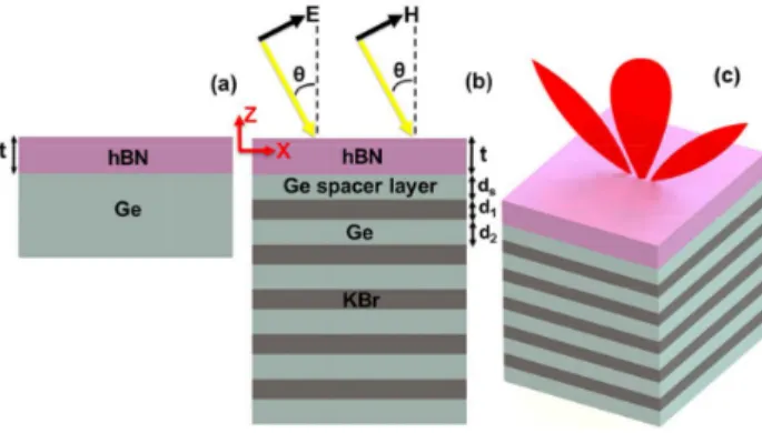
Figure 1(a) schematıcally represents a film of hBN of thickness t on top of a homogeneous Ge substrate with permittivity of εs. In panel (b) of Fig. 1, the film of hBN is transferred onto a 1D PC that comprises alternating layers of materials with a permittivity of ε1 and ε2 and a thickness of d1 and d2. The 1D PC and the film of hBN are separated with a Ge spacer layer
Fig. 1. Panels (a) and (b) illustrate a film of hBN with thickness t (placed in z=0) that is transferred onto a Ge substrate and onto a 1D PC, respectively. As shown in panel (b), the hBN-based 1D PC comprises alternating layers of KBr and Ge layers with the thicknesses d1 and dz and a spacer layer of Ge with the thickness ds. Panel (c) shows a three dimensional representation of the design and its coherent thermal emission at θ=0 and θ 45o
= .
Describing a film of hBN as a uniaxially anisotropic medium with a permittivity tensor of
t t z
( , , )
hBN diag
ε = ε ε ε and thickness t, y component of the magnetic field can be considered
as , , (z t/ 2) z z 1 2 (z t/ 2) , / 2 (z) , / 2 / 2. , / 2 a h TM h TM s q q q y q ae z t H h e h e t z t se z t − − − + > = + − ≤ ≤ < − (1)
By applying the appropriate boundary conditions for TM polarization [62], the dispersion relation of HPPs supported by the film of hBN can be formulated as [54–59]
' h,TM ' tan h(q t) . 1 a s a s Γ + Γ = − + Γ Γ (2) Here Γ =a qh TM, ε εa/ t aq , ' , / s qh TMε εs t sq Γ = , 2 2 0 a a q = β −ε β , 2 2 0 s s q = β −ε β , 2 2 , 0 / h TM x z z q =ε β −ε β ε , β0 =ω/ c, β =kt and 2 2 , , , 2 2 , [1 LO m TO m ], m t, z. m m TO m i m ω ω ε ε ω ω ω ∞ − = + = − − Γ (3)
Notice that εm becomes negative between ωTO m, andωLO m, phonon modes that makes the
in-plane and out-of-in-plane dielectric functions of hBN possess opposite signs in the lower- (upper-) frequency band, εz <0 and εt >0 (εz >0 and εz >0) that represents type-I (type-II) hyperbolicity [54–59]. Therefore, in Figs. 2(a) and 2(b), these bands are labeled as the RS-I and RS-RS-IRS-I regions. Therefore, the spatial dispersion of the modes that can propagate inside a film of hBN with unbounded wavenumbers can be expressed as hyperbolic isofrequency
surfaces 2 2 2
, / / 0
h TM t z
medium and the spatial dispersion of the supported modes becomes spherical that can be described as 2 2 2 , 0 h TE t q +β =ε β , where 2 2 , 0 h TE t q = β −ε β .
It is well-known that the allowed and forbidden frequency regions (band gaps) of a 1D PC can be given by [58]
1, , 1, ,
B 1 1 2 2 1 1 2 2
2, , 2, ,
cos(K d) cos h( d ) cos h( d ) ( TE TM TE TM)sin h( d )sin h( d ) / 2
TE TM TE TM
F F
q q q q
F F
= + + (4)
Where Fi TM, =εi/qi and Fi TE, =qi and qi = β2−ε βi 02(i 1, 2)= and β β= 0sin( )θ where θ is the angle of incident light. As mentioned hereinabove, a 1D PC is capable of supporting surface waves for both TE and TM polarizations [44]. These modes are supported in the bandgap of the system. Therefore, by appropriately designing the photonic crystal, i.e. matching the RS-II band of hBN and bandgaps of the 1D PC, it is possible to couple phonon polaritons of hBN and SWs of the 1D PC in the hBN-based 1D PC. This structure is schematically illustrated in Fig. 1(b); we call these coupled modes Tamm phonons. Considering Hy as , , (z t/ 2) z z 1 2 (z t/ 2) (z t/ 2) 1 2 1 s TM 1 , / 2 , / 2 / 2 (z) , ( / 2 ) / 2 {sin h(q [z (t/ 2 )]) cos h(q [z (t/ 2 )]}, ( / 2 ) a h TM h TM s s q q q y q q s s s ae z t h e h e t z t H s e s e t d z t p d γ d z t d − − − − + + > + − ≤ ≤ = + − + ≤ < − + + + + + < − + (5)
and applying the appropriate boundary conditions for TM polarization at different interfaces, the dispersion of the Tamm phonons supported by the 1D hBN-based PC can be obtained using the direct-matching procedure which is applicable for electronic and photonic layered devices [48, 63] h,TM tan h(q t) . 1 s a s a Γ − Γ = − Γ Γ (6) Here, Γ =s qh TM, X3,TM /εt, 2 3,TM s(1 e q ds sX1,TM) / s 2,TM X =ε + − q X , 2 2,TM ( 1 e q ds sX1,TM) X = − + − , 1,TM 1 1/ 1 1 X = Γ + Γ − , Γ =1 qsε γ1 TM /q1εs and [47] 2 2 1 1 2 2 1 1 sin h(q d ) sin h(q d ) cos h(q d ) cos h(q d ) B B iK d TM TM iK d F e e γ = + − (7) where FTM =F2,TM /F1,TM.
Similar to plasmonic materials [64], phononic materials can support surface phonon-pholaritons only for TM polarization [65]. However, symmetrically patterned structures, i.e. 2D grating phononic/plasmonic systems, are capable of supporting plasmonic/phononic resonances [22] for both TE and TM polarization. Moreover, using Tamm plasmons/phonons of plasmonic-/phononic-based 1D PCs, it is possible to excite plasmonic [49–52] or phononic [45–47] resonances in unpatterned films. Here, in order to investigate phononic-photonic resonance absorptions for TE polarization in the structure illustrated in Fig. 1(b), we also formulate TE Tamm polaritons supported by the 1D hBN-based PC. To this aim, considering
y
E
as Eq. (7) and applying TE boundary conditions [59], we arrive at the following dispersion relation for the TE Tamm modes4 5 h,TE 4 5 tan h(q t) X X . X X − = + (8)
Here X4 = −( qh,TE−X3,TE)(qh,TE−qa), X5 = −( qh,TE+X3,TE)(qh,TE+qa),
2 3, ( 1 e s sX1, ) / 2, q d TE s TE TE X =q − + − X , 2 2, (1 e s sX1, ) q d TE TE X = + − , 1,TE ( /1 TE s) / ( 1/ TE s)
X = q γ +q −q γ +q and γTE can be calculated using Eq. (7) by replacing TE
F with FTM [66] where FTE =F1,TE/F2,TE. 3. Results and discussion
In this section, we illustrate and discuss the obtained results from the above mentioned analytical relations and compare them with the ones that are achieved by FDTD simulations [67]. In our calculations, we take ε =1 2.25 and ε =2 16, which correspond to the permittivity
values of KBr and Ge in the mid-IR region, respectively. These materials are lossless and exhibit almost constant refractive index within the range of our interest; i.e. 6.2 μm to 7.3 μm. In order to match the photonic bandgap of the 1D PC to the second RS band of hBN, we choose d1=923nm and d2=576nm. Moreover, for the sake of simplicity, the material of the spacer layer is taken to be Ge in our calculations. It should be mentioned, by taking the appropriate value for the thickness of the spacer layer, similar results can be obtained for a different arrangement of the layers in the photonic crystal for which
1 16,d1 576 ,nm 2 2.25
ε = = ε = and ε1=16,d1=576 ,nmε2 =2.25 . Initially, using Eq. (2), we investigate the dispersion of HPPs supported by the films of hBN with different thicknesses, i.e. t=300 nm, 500 nm, and 1 μm. The considered structure is schematically illustrated in Fig. 1(a).
Fig. 2. (a) and (b) illustrate real and imaginary parts of εt and εz of hBN within entire mid-IR region. Panels (c), (d), and (e), respectively, illustrate the dispersion of HPPs supported by 300 nm, 500 nm, and 1 μm films of hBN within the wavelength range of our interest. 6.2 μm to 7.3 μm is the RS-II region in which hBN shows hyperbolic response of the second type.
Type-I (ε <z 0 and ε >t 0) and type-II (ε >z 0 and ε <t 0) hyperbolic regions of hBN are shown in Fig. 2(a). As expected, the imaginary parts of εz and εt, which are illustrated in Fig. 2(b), exhibits sharp picks at the upper edges of the RS regions. This characteristic makes
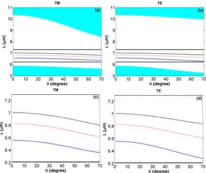
hBN a candidate for absorption applications within its RS bands that are located in the mid-IR region. In agreement with the previous studies [54–59], the dispersion of HPPs supported by 300 nm, 500 nm, and 1 μm films of hBN on Ge substrates are represented in Figs. 2(c)-2(e) within the upper RS band (RS-II). As seen from these panels, by increasing the width of the hBN film, the number of branches of the phononic modes is raised and the modes are shifted to lower wavelengths inside the RS-II band. Consequently, by appropriately choosing the hBN thickness, it is possible to tune the modes dispersion inside the RS region. It is noteworthy that, due to the support of type-I HPPs, a film of hBN can absorb light in the RS-I band for large angles of incident light for TM polarization, with and without the presence of a 1D PC. The presence of the 1D PC can only improve this absorption. More investigations prove that, by appropriately designing the 1D PC, it is possible to enhance the RH-I absorption up to 70 percent for TM polarization at only oblique incidences (θ>25o). On the other hand, as mentioned earlier, it is well-known that a 1D PC comprising dielectric layers is capable of supporting surface waves for both TE and TM polarizations [44]; these modes are supported in the bandgap of the PC. By properly choosing the thickness of Ge and KBr layers, it is possible to match the RS-II band of hBN and photonic bandgap of the 1D PC. Therefore, the phonons of hBN and SWs of the 1D PC can be efficiently coupled to create coupled photonic-phononic modes in the structure; i.e. Tamm phonons. As we mentioned earlier, our main aim in this paper is the investigation of light absorption/coherent thermal emission by the hBN-based 1D PC for different angles, which is schematically illustrated in Fig. 1(b). Consequently, in the next step, we examine the projected band structure and the supported Tamm phonons of the hBN-based 1D PC in Fig. 3 for incident angles smaller than 70 degrees that can be meaningfully realized by the ellipsometry measurements.
Fig. 3. Panels (a) and (b), respectively, show projected band structure of the 1D PC for TM and TE polarizations; the white and aqua regions depict photonic bandgaps and allowed the bands of the 1D PC. In these panels, dashed-dotted black (t=300 , 1.08 nm ds= μm), dotted red (t=500 , 1.03 nm ds= μm) and dashed blue (t=1 , 900 μm ds= nm) curves illustrate the coupled phononic-photonic modes (Tamm phonons) supported by the hBN-based 1D PC with different thickness of hBN films and the spacer layer. Solid black lines also indicate edges of the RS-II region of hBN which is placed within 6.2 μm to 7.3 μm. For illustrative purposes, magnified version of panels (a) and (b) are also illustrated in panels (c) and (d), respectively.
White and aqua regions in Figs. 3(a) and 3(b) illustrate allowed bands and forbidden regions of the 1D PC for TM and TE polarizations, respectively. The vertical solid lines in these panels show edges of the RS-II band of hBN which is extended from 6.2 μm to 7.3 μm. It is clearly observed from these figures that RS-II region of hBN is completely covered by the bandgap of the 1D PC for both TM and TE polarization and for the angles of incidence of
70o
θ < . Due to the interactions between the surface waves supported by the 1D PC and the phonons supported by the covered hBN film, some coupled phononic-photonic modes, Tamm phonons, can be supported by the system for 0≤ <θ 90o. Depending on the thickness of the hBN films, these couplings can be efficiently achieved by the proper thickness of the Ge spacer layer in-between the 1D PC and the hBN film. For the dispersion curves illustrated in Fig. 3 [plotted using Eqs. (6) and (8)], those thicknesses of the spacer layers are taken to be 1.08 μm, 1.03 μm, and 900 nm for 300 nm-, 500 nm-, and 1 μm-thick hBN cover layers, respectively. By these choices, the dispersions of Tamm phonons in Fig. 3 are more separated in the bandgap and, therefore, they are more illustratively recognizable. The procedures of the optimization of the spacer layer will be discussed later. Dashed-dotted black (t=300nm), dotted red (t=500nm), and dashed blue (t=1μm) curves in Figs. 3(a) and 3(b) correspond to the coupled modes supported in the bandgap of the hBN-based 1D PC. As it is clearly observed from these panels, these modes are supported in the RS-II region of hBN and are blue shifted by increasing the thickness of hBN, as it was expected from the results shown in Figs. 2(c)-2(e). In panels (c) and (d) of Fig. 3, dispersions of those Tamm modes are magnified for illustrative purposes.
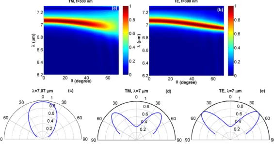
Fig. 4. Spectral-directional emissivity of the hBN-based 1D PC with t=300 nm and
1.08
s
d = μm for TM [panel (a)] and TE [panel (b)] polarizations. Angular distribution of the thermal emission of the structure at λ=7.07 mμ and λ=7 mμ are illustrated in panels (c), (d) [TM] and (e) [TE].
Now, we investigate the absorption characteristic of the hBN-based 1D PC for three different thicknesses of the hBN films (t=300 ,500nm nm and 1 mμ ). Note that, according to Kirchhoff’s law, the spectral-directional emissivity [( , )λ θ ] of a structure is the same as its spectral-directional absorptivity [A( , )λ θ where A= −1 (R T+ )]; as a couple of examples see [3, 30, 33, 36–38, 45–50]. Therefore, in the following, using FDTD simulations, we numerically illustrate the emissivity results of the mentioned structures that can also be
interpreted as the absorption of the structures under our consideration. In addition, it should be noted that we consider 10 Ge-KBr pairs in our numerical analysis. Panels (a) and (b) of Fig. 4 show the calculated emissivity of the hBN-based 1D PC for t=300nm and
1.08
s
d = μm.
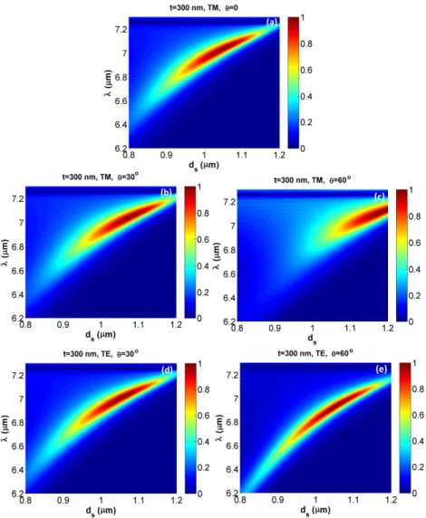
As is seen from panels (a) and (b) of Fig. 4, using a 300 nm-thick film of hBN on the 1D PC with Ge spacer of thickness 1.08 μm, it is possible to achieve nearly perfect coherent thermal emission (nearly perfect resonant absorption) for both TM and TE polarizations for angles smaller than 45o. For θ >45o TM thermal emission of the structure decreases while, for TE polarization, the absorption and consequently thermal emission are perfectly kept. In order to get more insight into the mechanism of the nearly perfect absorption/coherent thermal emission of the hBN-based 1D PC, we compare the numerical results illustrated in Figs. 4(a) and 4(b) with the analytical Tamm phonon dispersions of the structure that are illustrated by dotted-dashed black curves in Figs. 3(a) and 3(b). By this comparison, we understand that the nearly perfect resonant absorption is exactly due to the support of Tamm phonons that are the coupled photonic-phononic modes of the system. While a film of hBN on a homogeneous substrate supports HPPs only for TM polarization, the hBN-based 1D PC can support the Tamm phonons for both TE and TM polarizations, and this coupling leads to the perfect thermal emission for a wide angular range. This characteristic resembles the directing fluorescence and coherent thermal emision by metal-based 1D PCs [49–52] and SiC-based 1D PCs [45–47]. In order to get more insight into the coherent response of the system, the angular distribution of thermal emission of the structure at two different wavelengths (λ=7.07 mμ and λ=7 mμ ) are represented in Figs. 4(c)-4(e). As expected from the results shown in panels (a) and (b) of Fig. 4, at λ=7.07 mμ polar plot of the emissivity shows a wide thermal emission (angular width ∼70o) by the structure in the normal direction. Similarly, the angular distribution of the emissivity at λ=7 mμ for TM [Fig. 4(d)] and TE [Fig. 4(e)] polarizations also show a wide (angular width ∼37o) thermal emission by the structure at 45o. As mentioned earlier, the results illustrated in Fig. 4 were obtained for ds =1.08μm. This thickness is an optimal value for the thickness of Ge spacer in the hBN-based 1D PC for t=300nm. In Fig. 5, we explain how that value was taken as the optimal thickness of the Ge spacer layer.
Fig. 5. Thermal emission of the 1D hBN-based PC with t=300 nm for different thicknesses of the Ge spacer layer (ds). The results are illustrated for three critical angles and both polarizations; i.e. θ=0 [panel (a)], θ =30o [TE panel (b) and TM panel (d)] and θ=60o [TE panel (c) and TM panel (e)].
To optimize the thickness of the Ge spacer layer, we obtain the emissivity of the hBN-based 1D PC with t=300nm at three critical angles θ =0,θ=30o, and θ=60o for both TM and TE polarizations. The optimal value of ds is the one that gives us the maximum emissivity for all of three critical angles and both polarizations. From panels (a), (b), (d), and (e) of Fig. 5, it is observed that for ds =1.5μm, it is possible to achieve perfect emission for
0
θ = , θ =30o (TM and TE) and θ =60o (only TE), while for TM polarization at θ=60o the optimal value of ds is approx. 1.15 μm. Consequently, in order to keep the strength of thermal emission high enough for all the angles and both polarizations, we choose the optimal value of ds as 1.08 μm. For this thickness, the structure can absorb more than almost 70 percent of light for both TE and TM polarizations and for θ <550 (see panels (a) and (b) of
the system by changing the spacer thickness; i.e. by increasing ds the resonant frequency is red-shifted. Consequently, by appropriately choosing the thickness of hBN and the spacer layer, it is possible to achieve the desired resonant absorption within 6.2 μm to 7.3 μm.
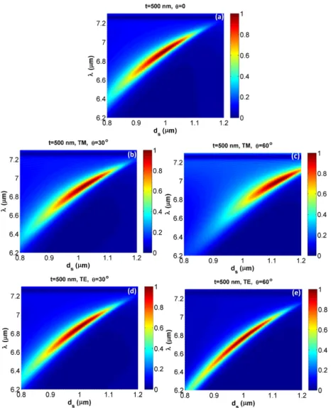
In the case for which the thickness of hBN and the spacer layer are taken as 500 nm and 1.03 μm, respectively, the spectral-directional emissivity of the hBN-based 1D PC is represented in Fig. 6.
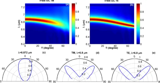
Fig. 6. Panels (a) and (b) respectively show TM and TE spectral-directional emissivity of the hBN-based 1D PC with t=500 nm and ds=1.03 μm. Angular distribution of thermal emission of the structure at λ=6.872 mμ and λ=6.8 mμ are illustrated in panels (c), (d) [TM] and (e) [TE].
The first point should be noticed about Figs. 6(a) and 6(b) is that by increasing the thickness of hBN from 300 nm to 500 nm, the perfect thermal emission region is shifted to shorter wavelengths. As it is obviously observed from these panels, the numerically calculated angular dispersion of the perfect thermal emission regions for TM and TE polarizations have been perfectly predicted by the analytically obtained dotted red dispersions of Tamm phonons in Fig. 3. Angular distributions of the spectral-directional emissivity of the structure for t = 300 nm and ds =1.03μm are illustrated in panels (c)-(e) of Fig. 6. Figure 7(a) shows that using the mentioned structure, it is possible to emit thermal energy at
6.872 m
λ= μ for normal incidence with angular width of almost 60o. Moreover, at
6.8 m
λ= μ thermal emission of this hBN-based 1D PC for TM [Fig. 6(d)] and TE [Fig. 6(e)] polarizations is more coherent (angular width~33o) than the previous case for which
300
t= nm. In order to obtain the optimal value for the thickness of the spacer layer for the case of t=500nm, we investigate the thermal emission of the system at θ =0, θ=30o and
60o
Fig. 7. Thermal emission of the 1D hBN-based PC with t 500nm= for the different thicknesses of the Ge spacer layer (ds). The results are illustrated for three critical angles and both polarizations; i.e. θ=0 [panel (a)], θ 30= o [TE panel (b) and TM panel (d)] and
o
θ=60 [TE panel (c) and TM panel (e)].
From the results shown in Fig. 7, it is seen that ds =1.025μm can be considered as the optimal value of the spacer layer for θ =0 [Fig. 7(a)], θ=30o for both polarizations [Figs. 7(b) and 7(d)] and θ =60o for TE polarization [Fig. 7(c)]. On the other hand, for
1.125
s
d = μm perfect thermal emission can be obtained for TM polarization at θ=60o. Therefore, in order to keep thermal emission high enough for both polarizations and all angles, we choose ds =1.05μm as the optimal thickness of the Ge spacer layer. The spectral-directional emissivity of the hBN-based 1D PC for t=500nm and ds =1.05μm is illustrated in Fig. 8. It is observed from this figure that using the mentioned system, nearly perfect resonant absorption and coherent thermal emission can be achieved for angles smaller than
50o
θ < . For θ >50o, while TE thermal emission is perfectly kept, TM emission is decreased but it is still more than 70 percent until θ =60o.
Fig. 8. TM [panel (a)] and TE [panel (b)] spectral-directional thermal emission for the hBN-based 1D PC with t=500nm and the optimal value of thickness of the Ge spacer layer; i.e.
1.05
s
d = μm.
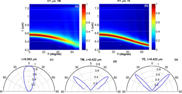
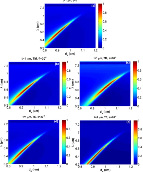
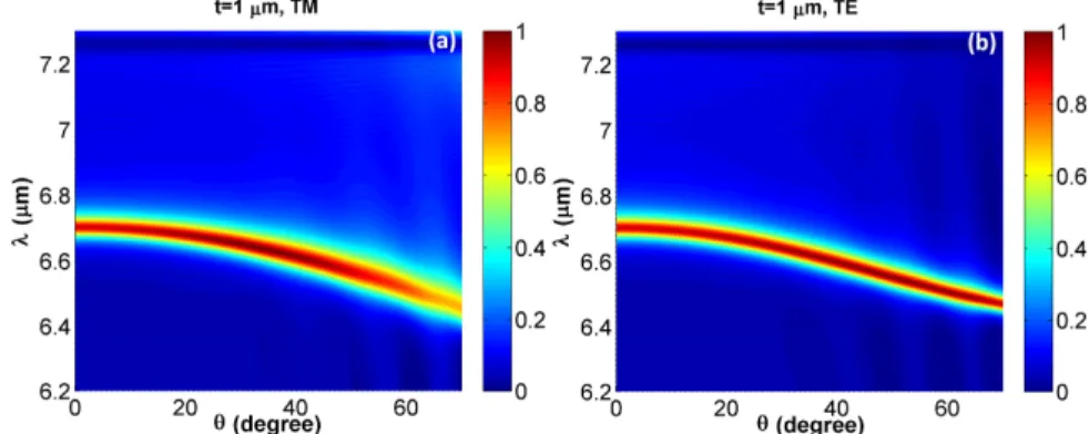
The last case we would like to investigate is the hBN-based 1D PC with t=1μm. First, we study the results for ds=0.9μm in Fig. 9.
Fig. 9. Spectral-directional emissivity of the hBN-based 1D PC with t=1μm and
0.9
s
d = μm for TM [panel (a)] and TE [panel (b)] polarizations. Angular distribution of thermal emission of the structure at λ=6.563 mμ and λ=6.422 mμ are illustrated in panels (c), (d) [TM] and (e) [TE].
It is observed that, similar to the previous two cases, there is a perfect match between the analytically obtained dispersion of the Tamm phonons shown by dashed blue curves in Fig. 3 and the resonant perfect thermal emission illustrated in panels (a) and (b) of Fig. 9. This match once more recalls this point that the coupling between phononic modes of hBN and confined photonic modes of the 1D PC is responsible for the observation of nearly perfect resonant absorption/thermal emission by the structure. Moreover, Fig. 9(c) shows that it is possible to achieve a coherent thermal emission by this structure at λ=6.563 mμ with an angular width of almost 36o. Angular distribution of the thermal emission of the structure at
6.422 m
λ= μ illustrates that coherent thermal emission by the angular width of 20o [Fig. 9(d)] and 15o [Fig. 9(e)] can be obtained by the hBN-based 1D PC for t=1μm.
Consequently, for this case, thermal emission by the structure is considerably more coherent than the previous cases for which 500 nm and 300 nm films of hBN were considered in the structure.
Fig. 10. Thermal emission of the 1D hBN-based PC with t 1μm= for different thicknesses of the Ge spacer layer (ds). The results are illustrated for three critical angles and both polarizations; i.e. θ 0= [panel (a)], θ 30= o [TE panel (b) and TM panel (d)] and θ=60o
[TE panel (c) and TM panel (e)].
Like the previous two structures, in order to be able to find the optimal thickness of the Ge spacer layer for t=1μm hBN-based 1D PC, we investigate the thermal emission of the structure for the different values of ds at those three critical angles for both polarizations. According to panels (a), (b), (d), and (e) of Fig. 10, by taking ds as 0.92 μm, maximum thermal emission for θ=0, θ =30o (TE and TM) and θ=60o (TE) can be obtained. On the other hand, with ds =1.03μm, the structure shows the best response for TM polarization at
60o
the Ge spacer layer in order to get the best response from the hBN-based 1D PC with 1
t= μm at all angles. TM and TE spectral-directional emissivity for the optimal design are represented in Fig. 11.
Fig. 11. Panels (a) and (b), respectively, present TM and TE spectral-directional thermal emission of t=1μm hBN-based 1D PC with ds =0.95μm as the optimal value of
thickness of the Ge spacer layer.
As it is seen from panel (a) of Fig. 11, the hBN-based 1D PC with t=1μm and 0.95
s
d = μm shows nearly perfect TM resonant absorption/coherent thermal emission for 55o
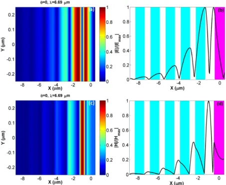
θ < and the emission is maintained over 70 percent for θ <70o. Figure 11(b) once more reminds us that these unpatterned structures (i.e. hBN-based 1D PCs with t=300nm, 500 nm and 1 mμ ) depict nearly perfect TE coherent emission for all the angles of incidences. In order to improve our description of the mechanism of light absorption and coherent thermal emission by the system, in the last figure we investigate profiles of a Tamm phonon, for
0
θ = and λ=6.69 mμ . Notice that mode profiles for the θ=30o and θ=60o are similar to the one of θ =0.
In contradiction with Tamm plasmons for which the electric field is localized in the dielectric below the metal film [49–52], mode profiles in Fig. 12 illustrate that for Tamm phonons the magnetic field is localized inside the spacer layer below the phononic film. It is seen from the mode profiles that the incident light can excite a Tamm mode that vanishes within five periods inside the structure. As a complementary discussion, it should be reminded that to the present, using isotropic phononic (e.g. SiC) [45–47] and plasmonic (e.g. Ag) materials [49–52], it has been theoretically and experimentally proved that the coherent thermal emission can be obtained by truncated 1D PCs operating in the far-IR and a window within the mid-IR region (10-12 μm). The physics behind all these works are the support of Tamm plasmons/phonons by the Ag-based and SiC-based 1D PCs. In the present study, first, we have explicitly derived dispersion of Tamm phonons supported by hBN as a uniaxially anisotropic material on a truncated 1D PC for both polarizations and verified our analytical results by FDTD simulations. Second, the operating wavelength of the considered structures in this manuscript (6.2 to 7.3 μm) makes the potential application of the hBN-based 1D PCs completely distinguishable from those similar Ag-based and SiC-based systems. Moreover, as mentioned earlier, due to the support of HPPs in the RS-I band of hBN, this material is also capable of light absorption at oblique incidences for TM polarization. By an appropriate design, this absorption can be enhanced up to 70 percent in the hBN-based 1D PCs. Thus, these hybrid systems can operate simultaneously in two separate absorption windows in the mid-IR range.
Fig. 12. Panels (a) and (c), respectively, illustrate normalized |E| and |H| mode profiles of a Tamm phonon supported by t=1μm hBN-based 1D PC with ds =0.95μm at
0
θ= and λ =6.69 mμ . Panels (b) and (d) show the corresponding line plots of the normalized |E| and |H|.
4. Conclusion
In conclusion, we have theoretically shown that hBN-based 1D PCs are capable of perfectly absorbing mid-IR light in a wide angular range and can behave as coherent thermal emitters for both polarizations. These optimized structures are made of unpatterned films of hBN on top of a 1D PC that is composed of alternating layers of KBr and Ge with a Ge spacer layer. Based on analytical calculations, we have investigated coupled photonic-phononic modes supported by the mentioned hBN-based devices; i.e. Tamm phonon modes. In support of the analytical results, our numerical findings have proven that the perfect light absorption is achieved due to the support of Tamm phonons by the structure. We have found that, with optimal designs according to the thickness of hBN films, it is possible to resonantly absorb light within 6.2 μm to 7.3 μm for both polarizations in a wide angular range. However, the device based on 1 μm-thick film of hBN is the best candidate for a nearly perfect coherent thermal emitter.
Funding
Scientific and Technological Research Council of Turkey (TUBITAK) (113E331); DPT-HAMIT (14E374 and 109E301).
Acknowledgments
One of the authors (E.O.) also acknowledges partial support from the Turkish Academy of Sciences.