Journal of Natural and Applied Sciences Volume 21, Issue 1, 235‐240, 2017 Fen Bilimleri Enstitüsü Dergisi Cilt 21, Sayı 1, 235‐240, 2017 DOI: 10.19113/sdufbed.58096
Analysis of the Mosaic Defects in Graded and Non Graded In
xGa
1‐xN Solar Cell Structures
İlknur KARS DURUKAN*1, Mustafa Kemal ÖZTÜRK2,3, Süleyman ÖZÇELİK2,3, Ekmel ÖZBAY4
1Gazi University, Life Sciences Research and Application Center, 06830, Ankara 2Gazi University, Department of Physics, 06500, Ankara 3Gazi University, Photonics Research Center, 06500, Ankara 4Bilkent University, Department of Physics, 06800, Ankara (Alınış / Received: 23.06.2016, Kabul / Accepted: 04.01.2017, Online Yayınlanma / Published Online: 03.02.2017)
Keywords InGaN/GaN, Solar cell, MOCVD, HRXRD, UV, XRD Abstract: In this study, graded (A) InxGa1‐xN (10.5 ≤ x ≤ 18.4) and non graded (B)
InxGa1‐xN (13.6 ≤ x ≤ 24.9) samples are grown on c‐oriented sapphire substrate
using the Metal Organic Chemical Vapour Deposition (MOCVD) technique. The structural, optical and electrical features of the grown InGaN/GaN solar cell structures are analyzed using High Resolution X‐Ray Diffraction (HRXRD), Photoluminescense (PL), Ultraviolet (UV), current density and potential (JV) measurements. According to the HRXRD results; it is determined that the InGaN layer of the graded structure has a lower FWHM (Full width at half maximum) value. From the PL measurements, it is observed that the GaN half‐width peak value of the graded sample is narrower and the InGaN peak width value of the graded sample is larger. From UV measurements, that the graded sample has a greater band range. JV measurements determine that the performance of the graded structure is higher.
Dereceli ve Derecesiz In
XGa
1‐XN Güneş Hücresi Yapılarındaki Mozaik Kusurların Analizi
Anahtar Kelimeler InGaN/GaN, Güneş hücresi, MOCVD, HRXRD, UV, XRD Özet: Bu çalışmada, dereceli InxGa1‐xN (A) (10.5 ≤ x ≤ 18.4) ve derecesiz (B) InxGa1‐ xN (13.6 ≤ x ≤ 24.9) örnekleri c yönelimli safir alttaş üzerine Metal OrganikKimyasal Buhar Biriktirme Tekniği ile büyütüldü. InGaN/GaN güneş hücresi yapıları Yüksek Çözünürlüklü X‐Ray Kırınım(HRXRD), Fotolüminesans (PL) ve Ultraviyole (UV), Akım yoğunluğu ve potansiyel ölçümleri (JV) ile analiz edildi. XRD sonuçlarına göre dereceli InGaN yapısı düşük FWHM değerlerine sahiptir. PL ölçümlerinde ise dereceli yapıdaki GaN’ın ortalama yarıgenişlik değeri daha dar ve InGaN’ ın pik genişliği dereceli yapı olması nedeniyle daha geniştir. UV ölçümlerinden dereceli yapının genişleyen bant aralığına sahip olduğu görüldü. JV ölçümlerinden ise dereceli yapının performansının daha yüksek olduğu belirlendi. 1. Introduction
Because of the applications at light emitting diodes (LEDs), laser diodes and light sensors, AlN, GaN, InN and the III‐N material system containing these have a wide usage [1,2]. Meanwhile the band range of the InN alloy and the band range of the InGaN material reach almost respectively 0.65 eV from infrared to the ultraviolet areas [3‐5]. This direct and wide band range made InGaN material suitable for photovoltaic applications. This range gives a opportunity for not only constucting high efficient multi joint sun battaries, also creates an possibility to manufacture a third generation device that bases on a interband solar cells made up of only nitrogen material [6,7].
It is determined that the maximum efficiency regarding solar cell for a three‐junction GaInP‐ GaInAs‐Ge structure at 1.5 AM (AirMass) 200x sun is 37.4% [8]. It is conluded that such devices will have widespread usage because they are useful in terms of efficiency limits [9]. According to the detailed balance modelling, we can increase terrestrial practical photovoltaic efficiency of more than 50 % only by using the materials that have band range greater than 2.4 eV [10]. In addition to the wide band ranges, nitrides also provides suitable photovoltaic features including lower effective carrier loads, higher mobility, higher peaks and saturation velocities, higher absorption coefficients and radiation tolerances [11]. The III‐N technology is suitable for growing high qualitative crystal structures and
manufacturing optoelectronic devices which supports the potential of high efficient photovoltaic structures.
Due to to the existing technological challenges of the solar cell production and the additional requirements faced during the manufacture of solar cell, The InGaN solar cell technology remains as a widely undiscovered application and continues to be important. In this study, we are presented graded InxGa1‐xN (10.5 ≤ x ≤ 18.4) and non graded InxGa1‐xN
(13.6 ≤ x ≤ 24.9) samples with various In compositions grown on a c‐oriented sapphire substrate using the MOCVD technique. The structural, optical and electrical features of the grown InGaN/GaN solar cell structures are analyzed by a HRXRD, PL, UV. JV measurements and the solar battery performance of the grown structures are discussed in detail.
2. Material and Method
The structural properties of the samples were characterized by the high‐resolution X‐ray diffraction (HRXRD) technique using a Bruker D8 system, delivering a CuK1 line. PL measurements were taken
by using the JobinYvon Florong‐550 PL system with a 50‐mW He‐Cd laser (λ= 325 nm) as excitation light source at room temperature. The current voltage characteristics were performed using a Keithley 4200 source‐meter, and an OrielSoll A class AAA solar simulator. The UV–vis optical transmission spectra of the InGaN/GaN solar cell structures were measured using a lambda 2S Perkin Elmer UV–vis spectrometer at room temperature. 2.1. Growing conditions InGaN/GaN solar cell structures (Figure 1) are grown by the MOCVD technique on a c‐oriented sapphire substrate. The epitaxial film is cleaned under H2 gas
at 1100C degree for 10 minutes. In the first epitaxial growth process, GaN nucleation layer(10 nm) are grown at 575C degree [12, 13]. The TMGa flow rate is adjusted to 10 sccm, NH3 flow rate to 1500 sccm
and the growing pressure is 200 mbar. Following the completion of growing of the nucleation layer, the GaN buffer layer is grown at 1070C degree. The growth of the buffer layer is provided by keeping the TMGa flow rate stable at 15 sccm, the NH3 flow rate at
1800 sccm and the growing pressure is 200 mbar. The thickness of the GaN buffer layer is 1.6 µm. The growing process is endured by releasing the SiH4
source and an n‐type GaN layer is obtained whereby the SiH4 source. The SiH4 source has attenuated
features throughout the MOCVD process. Furthermore, the flow rate of the SiH4 source is 10
sccm. The InxGa1‐xN active layers are grown in
samples A and B at temperatures between 745‐760C degree and an In flow rate of 75 sccm in between n‐ and‐p contact layers over nucleation and buffer. For
this and other layers, NH3 flow rate to 5000 sccm and
the growing pressure is 200 mbar for N source. While the thicknesses of InGaN layer in sample A are 25 nm (graded) and 200 nm (non graded), the InGaN layer (non graded) is 220 nm thickness. The active layers are grown as 1.9 µm thickness between p‐type InGaN and n‐type GaN contact layers. The p+ InGaN layer is grown using a Mg doping source. The flow rate of this source is 35 sccm. During the growth of the InGaN layer were the sources, which were open during the growth and the other layers kept closed. The Mg flow rate is adjusted to 40 sccm in order to provide more doping. The InGaN layer ratio is converted to a graded status by keeping the InGaN layers in forbidden energy band range’s. In flow rate used for the active layer continuous.
p contact InGaN layer t=70 nm Graded InGaN layer t=25 nm Non graded InGaN layer t=200 nm
n contact GaN layer t= 1.9 µm GaN buffer layer t=1.6 µm GaN nucleation layer t=10 nm
Al2O3 substrate (a) (b) Figure 1. The InGaN solar cell structure has a thickness of t in the figure. Two sample structures with a) InGaN graded (sample A) and b) InGaN non graded (sample B) 3. Results 3.1. XRD analysis Figure 2 shows the omega scans of samples A and B. It is seen that the Bragg peaks for the crystal planes regarding the InGaN and GaN layers from (002), (004) and (006) for both samples.
The half‐widths of the diffraction peaks reflect the crystal quality of the InGaN and GaN layers. Increasing of plane tilt angle and twist angle and limited crystal dimensions result in the expansion of these peaks. FWHM of the symmetric peaks for the InGaN and GaN indicated in Figure 2 are shown in Table 1. When the measured values are compared, it is seen that the GaN peak half‐width for the symmetric planes of both samples are almost equal. Because both samples have similar growing
p contact InGaN layer t=70 nm Non graded InGaN layer t=220 nm
n contact GaN layer t= 1.9 µm GaN buffer layer t=1.6 µm GaN nucleation layer t=10 nm
conditions. However the InGaN layer of sample A has a lower FWHM value compared when with sample B. This clearly indicates that the InGaN layer in sample A has a higher crystal quality. Figure 2. Omega curve of sample A and B in wide angle
X‐Ray reflection’s peak broadening of the InGaN at sample A is 141 cps, and more than 32 cps at sample B. This result corresponds with the peak half‐width result. In the findings, it is determined that sample A has a better crystal quality.
Table 1. The peak positions and the FWHM values of the
symmetric planes (002) and (004) of the GaN and InGaN layers of sample A and sample B
3.2. PL analysis
InGaN is a group‐III nitride material. The usage of InGaN in the solar cell production is considerably advantageous. Because it provides a sufficient performance for low dimensional systems due to a nitride containing material. In addition to this, such nitride containing materials have a long life span at high temperatures, pressure and frequency values. InGaN alloy is one of the materials with a forbidden energy band range, which lower than 2.0 eV and its forbidden energy band range can be adjusted between 0.7 eV (InN) and 3.4 eV (GaN) depending on its Indium factor [14,15]. Moreover, InGaN structures have direct forbidden energy band range and strong absorption coefficient. Thus, InGaN structures are ideal candidates for solar cell manufacture.
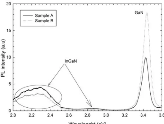
The photoluminescence (PL) spectrums of the samples A and B at room temperature are shown in Figure 3. As seen in the figure, the stimulation peak of 3.4 eV to the GaN layer exists. The broad stimulation
peak ranging from 1.9 to 2.6 eV (PL) is belonged to InGaN. Figure 3. PL graphics for sample A and sample B An intervension occurs because the forbidden energy band ranges of the P contact InGaN layers and non graded InGaN are close to each other. Intervention peaks are observed for InGaN from 1.9 to ‐2.6 eV ranges. Beside this, a PL emission peak of the in graded layer is observed in sample A at around 2.9 eV [16,17]. However, no peak of the in graded layer is observed in the HRXRD.
As shown in Figure 3, there is a change of the peak position due to graded sample A resulted in an expansion of the GaN peak. Beside this, a stimulation peak of the InGaN phase is observed at around 2.9 eV. It is observed that the stimulation peaks of the InGaN layers and the graded InGaN interfere with each other because of being close. The peak position of sample A for the GaN layer is 3.4258, and 3.4432 in
sample B. The peak half‐width for GaN of sample A is 0.1333, the peak half‐width for GaN of sample B is
0.14075 and the peak half‐width for InGaN in sample A is 0.2544 [16,17]. 3.3. UV analysis The forbidden energy band range of the InN epitaxial layer is determined as 1.75 eV. This value is higher than the value determined previously (0.7 eV) [18]. There is an ongoing discussion about the forbidden energy band range of this layer although a lower forbidden energy band range was stated for InN. The forbidden energy band ranges for InN vary between 0.7 eV to 1.9 eV in the literature [19]. The forbidden energy band ranges of the InN epitaxial layers do not only depend on the growing techniques, but also on the carrier density [18]. Normally the Fermi level of doped semi conductors reaching transmitter level above is constituted by the increase of more transmitter level doping densities. This pushes the Fermi level to a higher energy level. Even it can reaches to the transmission band. This is called as Burstein‐Moss effect which is shown in equation 1 [18]. GaN layer InGaN layer A B A B Plane FWHM FWHM FWHM FWHM (°) (°) (°) (°) (°) (°) (°) (°) (002) 17.179 0.100 17.320 0.103 16.927 0.160 17.111 0.169 (004) 36.327 0.092 36.467 0.093 35.598 0.195 35.986 0.236
19 2 /3 0 * 0, 65 0, 0116( )( 10 ) g m E eV n eV m (1) In equation 1, m* is the mass of the free electron. This parameter depends on the density of the electron. mo is the mass of the vacuumed electron, and n is the density of the electron [21,22]. The Burstein‐Moss effect at wide value of the absorption edge increases as per the high carrier density. According to equation 2, if it exceeds a carrier density of 3x1020 cm‐3 t, an
extra energy is resulted due to the additional term indicated in equation 2.
1 1 (2)
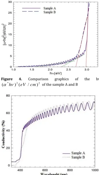
The InGaN epitaxial layer also provides a slightly higher absorption edge but the Burstein‐Moss effect is lower. Because of the bearer density of the InGaN, The epitaxial layer has a lower value than InN. The value of the forbidden energy range as a result of UV is estimated by the absorption edges of the films. The optical absorption constant α is derived from the [23]. Here α is the constant, h the Planck constant and ν the received radiation frequency. The forbidden energy band range is represented by Eg. m value is changed for direct and indirect transitions. In this study m is 2 since InGaN has a direct band transition. Figure 4 shows the graphics of (αhv)2 against hv. The Eg values of solar cell are obtained from this graphic. The forbidden energy band ranges of the solar cell are determined as 1.6‐2.9 and 1.7‐2.7 eV for sample A and B, respectively. Beside this, an inter phase is observed at 2.3 eV. Figure 5 shows the conductivity graphics of samples A and B.
3.4. JV analysis
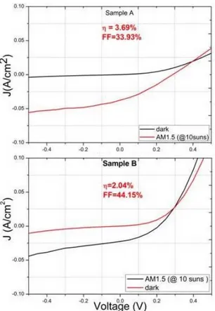
Electrical performance of a solar cell could be determined by current density versus voltage (J‐V) measurements, which is the most common technique in photovoltaics. In a typical J‐V characteristic of a solar cell under illumination, short circuit current density (Jsc), the current density at the maximum
power point (Jmmp), open circuit voltage (Voc) and
voltage at the maximum power point (Vmmp) parameters are used to calculate the efficiency of a solar cell and the fill factor (FF), defining by the ratio of power produced at the maximum power point devided by the product of Voc and Jsc for AM 1.5G
spectrum. These properties are obtained with (3) and
(4)typical J‐V characteristic of a solar cell is given in Figure 6. Since Voc value is close to zero in our study, it is a low performance. However this performance could be increased by making different designs [24]. In value is inversely proportional to Voc in InGaN
solar cell structures. Furthermore crystal imperfection in the structures changes the value of Voc depending on changing of In concentration at low
growing temperature [25].
Figure 4. Comparison graphics of the hv
* 2 2
( h ) (eV /cm) of the sample A and B
Figure 5. UV conductivity graphics of the graded and non
graded sample A and sample B wavelength
As shown in Figure 6, FF of sample A is lower than sample Bs. FF is defined by the ratio of power produced at the maximum power point divided by the product of Voc and Jsc. Having low FF value of InGaN solar structures is related to Voc value because the high carriers density affects band gap. Thus Voc
decreases. There are also other factors, which make decreasing of the FF value, as doping level and recombination [26].
Figure 6. J‐V characteristics of the sample A and B
According to the JV calculations the solar cell performances of the graded sample A and sample B are 3.69 % and 2.04 %, respectively. Increasing In content in active region of solar cells improve efficiency (η); but, increasing In content much within the active layer deteriorates efficiency. This is because of the decreasing crystal quality and increasing background electron concentration with increasing In content in the active layer of solar cells. In the light of these results, it is determined that the solar efficiency of sample A has a higher performance. These results correspond with the other HRXRD, PL and UV results. As a result, the continuous Indium flow indicates that the structural, optical and electrical features of sample A are better than that of sample B.
4. Discussion and Conclusion
In this study InGaN/GaN solar cell structures are grown on c‐oriented sapphire substrate by the MOCVD technique. The structural features of the samples A and B are anayzed by a HRXRD. FWHMs of the symmetric HRXRD omega peaks for the GaN and InGaN layers are compared. It is determined that the GaN half‐width peaks for the symmetric planes of both samples are nearly equal. This situation is an expected result since the GaN layers in both samples have similar growing conditions. However, the InGaN layer of sample A has a lower FWHM value than sample B. This also clearly shows that the InGaN layer at sample A has a higher crystal quality. The conductivity of samples A and B is determined by the UV measurements and the Eg values are obtained. The forbidden energy band ranges of the solar cell
are determined to be 1.6‐2.9 and 1.7‐2.7 eV for samples A and B respectively. In addition to this, an inter‐band phase is observed at 2.3 eV. According to the final conducted JV calculations the solar battery performance of the graded samples A and B are determined to be 3.69 % and 2.04 % respectively. These results correspond with the other HRXD, PL and UV results. As a result, it is determined that the structural, optical and electrical features of sample A with a continuous Indium flow or sample A graded In, are better than that of sample B. According to these results, it is determined that sample A, which is a graded structure that can be used for the manufacturing of solar cell, has a higher efficiency and can operate with a high performance.
References
[1] Nakamura, S., Pearton, S., Fasol, G. 2000.The Blue Laser Diode, Springer, Berlin,56s.
[2] Arslan, E., Demirel, P., Cakmak, H., Ozturk, M.K., Ozbay, E. 2014. Mosaic Structure Characterization of the AlInN Layer Grown on Sapphire Substrate. Advances in Materials Science and Engineering, 2014, 1‐11.
[3] Davydov, V.Yu., Klochikhin, A.A., Seisyan, R.P., Emtsev, V.V., Ivanov, S.V., Bechstedt, F., Furthmuller, J., Harima, H., Mudryi, A.V., Aderhold, J. , Semchinova, O., Graul, J. 2002. Absorption and Emission of Hexagonal InN Evidence of Narrow Fundamental Band Gap. Phys. Status Solidi B, 229,R1‐R3.
[4] Wu., J., Walukiewicz., W., Yu., K. M., Ager III., J. W., Haller, E.E., Lu, Schaff, H. W. J.,Saito, Y. , Nanishi, Y. 2002. Unusual properties of the fundamental band gap of InN, Appl. Phys. Lett., 80, 3967‐3969.
[5] Matsuoka, T., Okamoto, H., Nakao, M., Harima, H., Kurimoto, E. 2002. Optical bandgap energy of wurtzite InN. Appl. Phys. Lett., 81,1246‐1248. [6] Omkar, J., Ian, F. 2007. Design and
characterization of GaN/InGaN solar cells. Appl.Phys.Lett., 91, 1‐3.
[7] Luque, A., Marti, A. 2001. A metallic intermediate band high efficiency solar cell. Prog. Photovoltaics, 9, 73‐86.
[8] Yamaguchi, M., Takamoto, T., Araki, K. 2006. Super high‐efficiency multi‐junction and concentrator solar cells. Solar Energy Mater Solar Cells, 90(18,19), 3068–3077. [9] King, R. R., Law, D. C., Edmondson, K. M., Fetzer, C. M., Kinsey, G. S., Yoon, H., Sherif, R. A., Karam, N. H. 2007. 40% efficient metamorphic GaInP/GaInAs/Ge multijunction solar cells. App. Phys. Lett., 90, 1‐3.
[10] De Vos, A. 1992. Endoreversible Thermodynamics of Solar Energy Conversion, Oxford University Press, Oxford, 90s.
[11] Nanishi, Y., Saito, Y., Yamaguchi, T. 2003. RF‐ Molecular Beam Epitaxy Growth and Properties of InN and Related Alloys. Jpn. J. Appl. Phys., 142, 2549‐2559.
[12] Ugo, L. et al. 2012. Increasing the reliability of solid state lighting system via self healing approaches. Microelectronic Reliability, 52(1),71‐89.
[13] Kendrick Chito, E. 2008. Revisiting Nitride Semiconductors, Epilayers, p‐type Doping and Nanowires. University of Canterbury, Electrical and Electronic Engineering, NewZeland, 49s. [14] Brown, G.F., Ager III, J.W., Walukiewicz, W., Wu,
J. 2010. Finite element simulations of compositionally graded InGaN solar cells. Solar Energy Materials and Solar Cells, 94, 478‐483. [15] Yamaguchi, T., Morioka, C., Mizuo, K., Hori, M.,
Araki, T., Nanishi, Y., Suzuki, A. 2003. Growth of InN and InGaN on Si substrate for solar cell applications, Compound Semiconductors: Post‐ Conference Proceedings International Symposium, 25‐27 August, USA, 214.
[16] Hu, C., Lo, I, Hsu, Y.,Shih, C., Pang, W., Wang, Y., Lin, Y., Yang, C., Tsai, C., Hsu, G. Z. L. 2016. Growth of InGaN/GaN quantum wells with graded InGaN buffer for green to yellow light emitters Japanese Journal of Applied Physics, 55(8),1‐6.
[17] Sun, Y., Cho, Y., Suh, E.K., Lee, H. J., Choi, R.J., Hahn, Y.B. 2003. High brightness blue and green light emitting quantum wells with graded‐In content profile grown by MOCVD,Phys. stat. sol. (c),7,2270‐2273.
[18] Schuster, M., Gervais, P. O., Jobst, B., Hosler, W., Averbeck, R., Riechert, H., Iberlkand, A., Stommer, R. 1999. Determination of the chemical composition of distorted InGaN GaN heterostructures from x‐ray diffraction data. Journal of Physics D‐Applied Physics, 32(10A), A56‐A60.
[19] Butcher, K.S.A., Tansley, T.L. 2005. InN latest development and a review of the band‐gap controversy, Superlattices and Microstructures, 38(1), 1‐37.
[20] Zhu, X.L., Guo, L.W., Yu, N.S., Peng, M.Z., Yan, J.F., Ge, B.H., Jia, H.Q., Chen, H., Zhou, J.M. 2006. Characteristics of High In‐content InGaN Alloys Grown by MOCVD, Chinese Physics Letters, 23(12), 3369‐3371.
[21] Fu, S.P. 2004. Effective mass of InN epilayers. Applied Physics Letters, 85(9), 1523‐1525. [22] Wu, J., Walukiewicz, W., Li, S.X., Armitage, R., Ho,
J. C., . Weber, E. R, Haller, E. E., Lu, H., Schaff, W. J., Barcz, A., Jakiela R. 2004. Effects of electron concentration on the optical absorption edge of InN. Applied Physics Letters, 84(15), 2805‐2807.
[23] Pankove, J. I., Miller, E. I., Berkeyheiser, J. E. 1971. GaN Electroluminescent Diodes. RCA Review, 32(3), 383‐392.
[24] Valdueza‐Felip, S., Mukhtarova, A., Grenet, L., Bougerol, C., Durand, C., Eymery, J., Monroy, E. 2014. Improved conversion efficiency of as‐ grown InGaN/GaN quantum‐well solar cells for hybrid integration. Appl. Phys.Exp., 7, 1‐3. [25] Mahala, P., Behura, S. K., Ray, A., Dhanavantri, C.,
Jani, O. 2012. The Effect of Indium Composition on Open‐Circuit Voltage of InGaN Thin‐Film Solar Cell: An Analytical and Computer Simulation Study. AIP Conf. Proc., 1451, 85‐87. [26] Cai, X. M., Zeng, S. W., Li, X., Zhang, J. Y., Lin, S.,
Lin, A. K, Chen, M., Liu, W. J., Wu, S. X., Zhang, B.P. 2011. Dependence of the Property of InGaN p‐i‐n Solar Cells on the Light Concentration and Temperature. IEEE Transactions on electron devices, 58,3905‐3911.