© 2010 WILEY-VCH Verlag GmbH & Co. KGaA, Weinheim www.pss-rapid.com
pss
Phys. Status Solidi RRL 4, No. 10, 286 – 288 (2010) / DOI 10.1002/pssr.201004129
Metamaterial inspired
enhanced far-field transmission
through a subwavelength nano-hole
Kamil Boratay Alici*
and Ekmel Ozbay**
Nanotechnology Research Center, Department of Physics, Department of Electrical and Electronics Engineering, Bilkent University, Bilkent 06800, Ankara, Turkey
Received 7 April 2010, revised 26 May 2010, accepted 27 May 2010 Published online 2 June 2010
Keywords sub-wavelength optics, metamaterials, split ring resonators, nano-antenna
**Corresponding author: e-mail [email protected], Phone: +00 90 312 290 1018, Fax: +00 90 312 290 1015 ** e-mail [email protected], Phone: +00 90 312 290 1966, Fax: +00 90 312 290 1015
© 2010 WILEY-VCH Verlag GmbH & Co. KGaA, Weinheim
1 Introduction Artificial structures that act like mate-rials can show extraordinary properties that could result in a group of new devices and extensive control of electro-magnetic waves [1]. The unit cell size of these metamateri-als determines their narrow operation frequency band, which could be in microwave, millimeter-wave, THz, mid-IR, IR or visible [2–12]. The physical sizes of the consti-tuting elements were typically an order of magnitude smaller than the operation wavelength. The most common unit cell element is the split ring resonator (SRR), which is used as an inclusion for negative permeability media [2]. When the operation frequency is at the optical regime, metamaterial properties such as negative refraction, the re-versal of Cherenkov radiation, Doppler shift, cloaking and an enhanced magnetic response could lead to high per-formance and novel photonic devices in information and communication technologies. These include negative index material based superlenses, optical isolators, electro-optic modulators, and optical switches.
Bethe studied transmission through a subwavelength aperture and diffraction of light passing through an aper-ture of size much smaller than the incident wavelength in the 1940s. The transmission efficiency that is normalized to the aperture area depends on the aperture size in terms
of the wavelength of the incident electromagnetic wave [13]. Ebbesen et al. invented the surface plasmon aided enhanced transmission structure [14]. The results are useful in the fields of scanning nano-lithography, optical data storage, near-field optical microscopy, and bio-chemical sensing, as they yield a light spot beyond the dif-fraction limit with an enhanced transmission [14, 15]. In the present Letter, we exhibit for the first time in literature, an exciting design that incorporates deep subwavelength optical split ring resonators to enhance the transmitted power radiated to the far field passing through a subwave-length hole.
2 Methodology We started our analysis with nu-merical simulations of the magnetic metamaterial unit cells. We used the commercial software CST-Microwave Studio [16]. We fabricated two-dimensional arrays of SRRs by us-ing e-beam lithography techniques. At the optical regime, we used u-shaped SRRs due to fabrication limitations. We measured the test samples by using a homemade transmis-sion-reflection setup. The details of our design simulations, nano-fabrication technique and experimental methods are given in the Supporting Information (online at: www.pss-rapid.com).
In the present study, we first demonstrate the polarization and orientation dependent transmission response of split ring resonators at the infrared and visible band. Then, we numeri-cally demonstrate a configuration for the enhancement of power passing through an electrically small hole. By using
deep subwavelength optical split ring resonator antennas and couplers we achieved a 400-fold enhanced transmission from a subwavelength aperture area of the electrical size λ2/25. The power was transmitted to the far field with 3.9 dBi directivity at 300 THz.
Phys. Status Solidi RRL 4, No. 10 (2010) 287
www.pss-rapid.com © 2010 WILEY-VCH Verlag GmbH & Co. KGaA, Weinheim
Rapid Research Letter
Figure 1 (online colour at: www.pss-rapid.com) (a) Schematic
and parameters of the unit cell. (b) Scanning electron microscopy image of the fabricated array.
3 Results The unit cell parameters of the SRR are shown in Fig. 1(a). In Fig. 2, we can compare the simula-tion and experimental results for the configurasimula-tion that is to be studied in detail in the following section. The periods in the x and y directions were px = py = P = 330 nm, side
length of the SRR was A = 155 nm, arm length was
L = 104 nm, width of the arms was W = 39 nm, separation
between the arms was S = 77 nm and the coated metal thickness was H = 39.5 nm. At the optical regime, the dis-persion characteristics of metals play an important role. They were taken into account by fitting the complex metal permittivity values given in Palik [17] by using the Drude model. CST Drude model permittivity is given by the formula: ε ω( )=ε•+ω ω ωp2/
(
-ivc)
where ωp is the plasma frequency and νc is the collision frequency. Our fit to the Palik data implied ωp = 13 250 × 1012 rad/s andνc = 130 THz. We used this data set to model the disper-sion properties of silver in our simulations. However, we discovered from the experimental data that the collision frequency of our metal was 4.3 times larger. Despite this, we used the values of ωp and νc obtained from the fit of Palik data in the following theoretical analysis.
Figure 2 (online colour at: www.pss-rapid.com) Simulated and
measured transmission response of the sample SRR array.
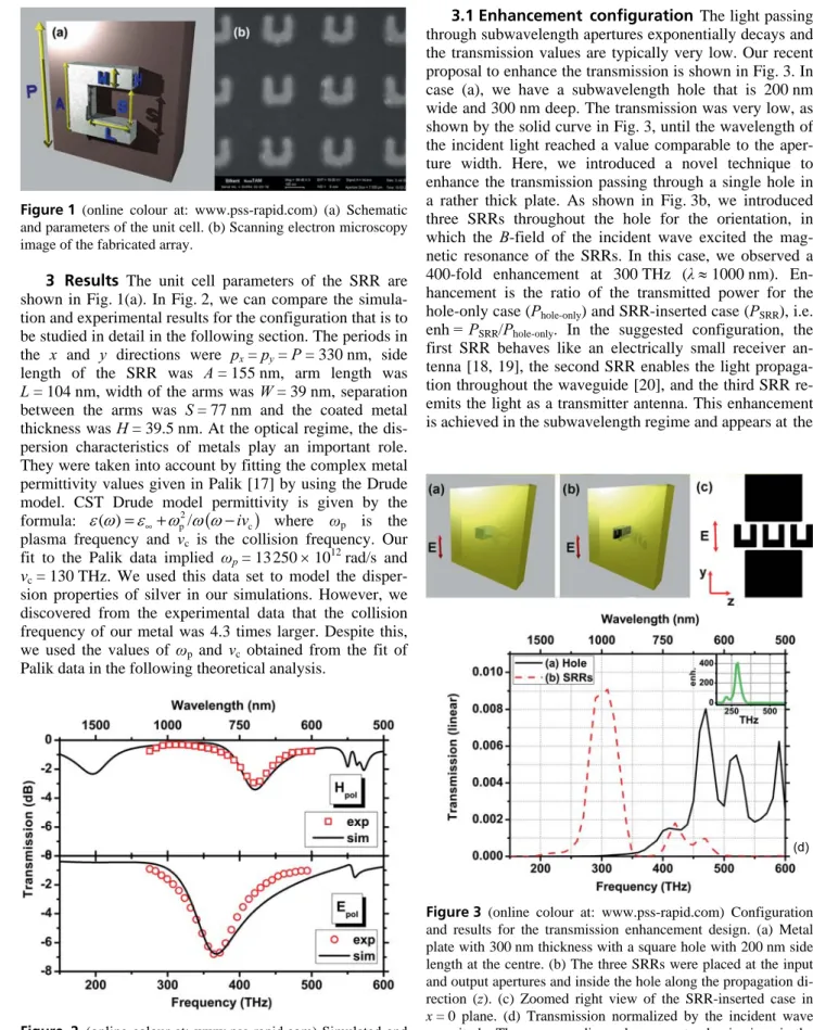
3.1 Enhancement configuration The light passing through subwavelength apertures exponentially decays and the transmission values are typically very low. Our recent proposal to enhance the transmission is shown in Fig. 3. In case (a), we have a subwavelength hole that is 200 nm wide and 300 nm deep. The transmission was very low, as shown by the solid curve in Fig. 3, until the wavelength of the incident light reached a value comparable to the aper-ture width. Here, we introduced a novel technique to enhance the transmission passing through a single hole in a rather thick plate. As shown in Fig. 3b, we introduced three SRRs throughout the hole for the orientation, in which the B-field of the incident wave excited the mag-netic resonance of the SRRs. In this case, we observed a 400-fold enhancement at 300 THz (λ ≈ 1000 nm). En-hancement is the ratio of the transmitted power for the hole-only case (Phole-only) and SRR-inserted case (PSRR), i.e. enh = PSRR/Phole-only. In the suggested configuration, the first SRR behaves like an electrically small receiver an-tenna [18, 19], the second SRR enables the light propaga-tion throughout the waveguide [20], and the third SRR re-emits the light as a transmitter antenna. This enhancement is achieved in the subwavelength regime and appears at the
(d)
Figure 3 (online colour at: www.pss-rapid.com) Configuration
and results for the transmission enhancement design. (a) Metal plate with 300 nm thickness with a square hole with 200 nm side length at the centre. (b) The three SRRs were placed at the input and output apertures and inside the hole along the propagation di-rection (z). (c) Zoomed right view of the SRR-inserted case in x = 0 plane. (d) Transmission normalized by the incident wave magnitude. The corresponding enhancement value is given in the inset.
288 K. B. Alici and E. Ozbay: Metamaterial inspired enhanced transmission through a nano-hole
© 2010 WILEY-VCH Verlag GmbH & Co. KGaA, Weinheim www.pss-rapid.com
status solidi
physica
rrl
Figure 4 (online colour at: www.pss-rapid.com) Field
distribu-tions at 300 THz. Near field power distribudistribu-tions around the struc-ture in the basis planes: (a) x – z plane, (b) y – z plane. (c) Far field patterns cut in the two planes.
far field. We obtained the enhancement at 1000 nm wave-length and used the largest dimension of the source of ra-diation while calculating the radiating aperture area. In this case, it was the area of the square hole as the SRRs’ di-mensions were smaller. The edge length of the square was 200 nm which corresponds to λ/5 electrical length at 300 THz. To compare, we also simulated the Ebbesen structure, for which the single hole was surrounded by pe-riodic surface corrugations [14]. We saw that the magni-tude of the power transmission level was within the same range in terms of the order of magnitude. The enhancement for that case was approximately 13-fold, while the opera-tion wavelength was around 700 nm [14]. Moreover, there were five grooves with electrical size almost equal to operation wavelength (λ), thereby the effective radiating aperture area of the Ebbesen structure was 9λ × 9λ. There are two major advantages of our structure: (i) The beam can be transferred to far field with an order of magnitude larger enhancement (~ 400-fold). (ii) Our radiating aperture area was subwavelength λ/5 × λ/5 and approximately 2000 times smaller than the Ebbesen case. Therefore, in terms of transmission enhancement per radiating aperture area our structure is quite impressive. On the other hand, the disadvantages of this design are the following: (i) It is very difficult to operate at the visible or UV regimes due to the saturating response [21]. (ii) The fabrication via current e-beam lithography, FIB milling, and multistep coating is quite difficult and expensive.
In Fig. 4, we demonstrate the far field response and near field beam profiles at the operation frequency. In our numerical study, we excited the structure under test via a waveguide and extracted the normal transmission response from far field monitors. In Fig. 4, we show the power pat-terns in the x – z and y – z planes. The reflected power level is 20 dB higher than the transmitted one at the far field at a 300 THz operation frequency. The angular beam widths were 120° and 88° in the x – z and y – z planes, respectively. The beam was quite broad with 3.9 dBi directivity.
There are examples of transmission enhancement stud-ies at the microwave regime, which may look similar to what we have demonstrated here at first glance [22]. On the other hand, the enhancement study becomes a different problem as the frequency range reaches infrared and
opti-cal regimes. By presenting the optiopti-cal SRR antennas here, for the first time in literature, we achieved an enhanced signal at the far field. Moreover, for the previously demon-strated microwave transmission enhancement the thickness of the metal was much much smaller than the aperture radius. At the optical regime, as we are very close to the plasma frequency of the metals the thickness of the metal must be thick enough to obtain a metallic response and thereby the aperture radius is comparable to the metal thickness. The mechanism presented here is more advanced than the microwave analogues and provides enhancement through deep holes placed in thick metal plates.
4 Conclusion After numerical and experimental char-acterization, we incorporated the split ring resonators to provide an alternative solution to the problem of enhanced transmission. Compared to the Ebbesen results, we ob-tained a 31 times larger enhancement from a 2000 times smaller radiating aperture area. Furthermore, the fields were radiated to the far field with 3.9 dBi directivity, which is suitable for real world applications at the optical regime.
Acknowledgements This work is supported by the
Euro-pean Union under the projects EU-PHOME and EU-ECONAM, and by TUBITAK under the project nos. 107A004 and 107A012. One of the authors (E.O.) also acknowledges partial support from the Turkish Academy of Sciences.
References
[1] D. R. Smith et al., Science 305, 788 (2004).
[2] J. B. Pendry et al., IEEE Trans. Microwave Theory Tech.
47, 2075 (1999).
[3] M. C. K. Wiltshire et al., Science 291, 849 (2001).
[4] E. Ozbay et al., IEEE Trans. Antennas Propag. 51, 2592 (2003).
[5] K. B. Alici et al., Appl. Phys. Lett. 91, 071121 (2007). [6] K. B. Alici et al., IEEE J. Sel. Top. Quantum Electron. 16,
836 (2010).
[7] K. B. Alici et al., J. Phys. D, Appl. Phys. 41, 135011 (2008). [8] Hou-Tong Chen et al., Nature 444, 597 (2006).
[9] C. Enkrich et al., Phys. Rev. Lett. 95, 203901 (2005). [10] N. Katsarakis et al., Opt. Lett. 30, 1348 (2005). [11] L. Zhang et al., Photonics Nanostruct. 2, 155 (2004). [12] K. B. Alici et al., Photonics Nanostruct. 6, 102 (2008). [13] H. A. Bethe, Phys. Rev. 66, 163 (1944).
[14] C. Genet et al., Nature 445, 39 (2007). [15] E. Ozbay, Science 311, 189 (2006). [16] CST GmbH, Darmstadt, Germany (2009).
[17] E. D. Palik, Handbook of optical constants of solids (Acade-mic Press, San Diego, 1998).
[18] K. B. Alici et al., J. Appl. Phys. 101, 083104 (2007). [19] K. B. Alici et al., Phys. Status Solidi B 244, 1192 (2007). [20] R. Marques et al., IEEE Trans. Antennas Propag. 51, 2572
(2003).
[21] J. Zhou et al., Phys. Rev. Lett. 95, 223902 (2005). [22] K. Aydin et al., Phys. Rev. Lett. 102, 013904 (2009).