Hot electron effects in unipolar n-type submicron
structures based on
GaN,
AIN
and their
ternary alloys
C. Sevikand
C. BulutayAbstract: The authors present an analysis of impact ionisation (11) and related hot electron effects in submicron sized GaN, AIN and their ternary alloys, all o f which can support very high field regimes, reaching a few meg,xvolts per centimetre (MV/cm). The proposed high field transport methodology is based on the ensemble Monte Carlo technique, with all major scattering mechanisms incorporated. As a test-bed for understanding 11 and hot electron effects, an n+-n-n+ channel device is employed having a 0. I pm thick n-region. The time evolution of the electron density along the device is seen to display oscillations in the unintentionally doped n-region, until steady state is established. The fermionic degeneracy effects are observed to he operational especially at high fields within the anode n+-region. For AI,J3al -.&based systems, it can be noted that due to alloy scal.tering, carriers cannot acquire the velocities attained by the GaN and AIN counterparts. Finally: at very high fields I1 is shown to introduce a substantial energy loss mechanism for the energetic carriers that have just traversed the unintentionally doped n-region.
1 Introduction
GaN, AIN and their ternary alloys are becoming techno- logically important semiconductors, finding application in
high-power microelectronic devices such as CaiV/AIGaN HEMTs as well as in optoelectronic devic:es such as visible- and solar-blind AlGaN photodiodes. Impact ionisation (11) is an important process for all thesa devices subject to extreme electric fields. In the case of high- power devices, 11 is undesired leading to breakdown, whereas the operation of devices such as avalanche photodiodes relies on the 11 mechanism. The subject of this work is the analysis of I1 and related hot electron effects in GaN, AIN and their ternary alloys, all of which can support very high field regimes, reaching values of a few MV/cm.
Surprisingly, there has been, as yet, no published measurement of the 11 coefficient for the AI,Gal-,N system. To meet this demand from the computational side, very recently we analysed II in hulk A1G;iN alloys [I], whereas in this work, we focus on device-related aspects of I1 and hot electron effects. A useful
model
system for understanding hot electron effects is the unipolar n+-n-n+ homojunction channel, which is to some extent impractical as it gives rise to excessive current density. In the following Sections we explain our computational0 IEE, 2003
/E€ Pmceedinpr onlint no. 20030047 Dol: IO. IC49lip-opt:20030047 Paper receivcd I Ith November 2002
The authors are with the Departincnt of Physics, Bilkent University. Bilkent 06533, Ankara, Turkey
86
procedure and present the transient and steady-state hot electron phenomena taking place within this structure.
2 Computational approach
The proposed high-field transport methodology is based on the ensemble Monte Carlo technique [2], incorporating standard scattering processes: acoustic, non-polar and polar optical phonons, ionised impurity scattering,
as well as alloy and I1 scatterings. We include all of the valleys in the lowest two conduction bands, aidcd by empirical pseudopotential hand structure calculations
[3, 41. We further append an additional higher-lying free electron band to account for the remaining bands. Because the emphasis is on I I , the energy loss of
the impacting electrons is accurately modelled [I]. We employ more than 20000 electrons within the ensemble, for a total simulation time of about 7.5 ps.
The time interval to invoke the Poisson solver is taken to he 0.1 fs.
The subject of alloy scattering has
caused
much contro- versy over the years, which is still unsettled. In the case of group-Ill nitrides, Farahmand ef al. [ 5 ] dealt with this issue and reported that using the conduction band offset between the binary constituents as the alloy potential leads to an upper bound for alloy scattering. Being more conservative, for this value we prefer to use 0.91 eV, which is halfof the corresponding GaN/AIN conduction band offset. Another source of concern has to do with the particular implemen- tation of alloy scattering within the Monte Carlo simula- tion. Following Fischetti and Laux [6], we treat the alloy scattering as an intra-valley process with the distribution of the final scattering angles assumed to be isotropic, even though at higher energies it attains a forward directional /€E Proe.-Oproe/romn, Wl. 150, No. I . Fehruov 2003character, which should presumably, weaken the effect of this mechanism on momentum relaxation. Therefore, we are led to think that the effect of alloy scattering may still be overestimated.
3 Results
To highlight the high-field transport phenomena in GaN, AIN or AI,TGal_,N based stmcturcs with submicron sized dimensions we consider a simple n+-n-n+ homojunction channel device [7] having 0. I pm thick unintentionally doped n-region sandwiched between two heavily doped ( 5 x 1 O I 8 cm-') ®ions of thickness at least 0.2 pm. Fig. 1 shows the velocity profiles for these materials; the Alo.4Gao.6N-based structure suffers severely from alloy scattering and has a much reduced velocity. If we turn off the alloy scattering, then the curve for Ala4Gao.6N (not shown) almost coincides with that for GaN. Previous analysis of hulk AlGaN alloys has shown that alloy scattering can modifp the high-energy electron distribution and lead to an increased I1 threshold [I].
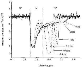
The electric field along this devicc is distributed highly non-uniformly, reaching a values of a few MV/cm, which peaks at the right nn+ interface, as shown in Fig. 2 . Also note the penetration of the electric field into the heavily doped anode ni-region with increasing applied bias, which amounts to widening of the unintentionally n-doped 'base' region, as in the Kirk effect. The time evolution ofthe electron density profile is depicted in Fig. 3 starting at 0.4 ps. Oscillations around the unintentionally doped n-region are clearly visible until steady state is established (7.5 ps curve in Fig. 3). Fermionic degeneracy effects are seen to be operational at high fields and at high concentration spots. We make usc of the Lugli-Ferry recipe [8] to account for degeneracy. However, if degene- racy is ignored, the electron distribution is observed to develop a dip in the n+-anode region, shown in Fig. 4. At a higher applied bias (80 V in GaN) the effect of II becomes dominant. As illustrated in Fig. 5 , this mechanism introduces a substantial energy loss mechanism for those energetic carriers that have just traversed the unintention- ally doped n-region.
0 0 1 0 2 0 3 0 4 0 5 0 6 distance, pm
Fig. 1
hius of 20 V
Vrlocity distribution over n+-n-n+ chunnel under applied
N i [ N N+ ti 3.5 E 3.0- 2.5 ~ 5
"
2.0- 1.50-$
c .- L I 1.01 0.1 0.2 0.3 0.4 0.5 distance, ~ r nFig. 2 Eleclricfield distribution over n+-n-nc GoN channel at
applied bioses rangiiig,from 5 V io 50 V
0.1 0.2 0.3 0.4 0.5 0.6
distance. pm
Time evolution of transient electron density profile over Fig. 3
n+-n-n+ GaN channel under applied bias of50 V
Stcady-state result is also shown, evaluated at 1.5 ps
04
0.1 0.2 0.3 0.4 0.5 0.6
distance. pm
Fig. 4 Steudy-state density ptnfile af hius of 50 I! x,ith and
withour degeneracy effeeci.y included
Nt I N
0 .
,--_
,'
', Ntfields I1 is shown to introduce a substantial energy loss mechanism for the encrgetic carriers that have just traversed the unintentionally doped n-region.
4 Summary
We have studied high-field transport in submicron sized n-doped unipolar structures. Alloy scattering in the case of AI,Ga,-,N is observed to be effective. Similarly, degeneracy effects are seen to he operational at high fields and in densely populated regions. Non-uniform electric field profiles and transient evolution of the clectron density along thc device are analysed. Finally, at very high
5 Acknowledgments
This work is supported by The Scientific and Technical Research Council of Turkey (TUBITAK).
6 References
I 2
BULUTAY. C.: 'Eleclron initiated impact innkation in AlCaN alloys',
Semicond. .Pi. k h n u i . . 2002, 17, (IO), pp. L5Y-1.62
FAWCETT, W., BOARDMAN, A.D.. and SWAIN, S.: 'Montc Carlo determination of electron transport properties in gallium arsenide'. J P$s. Chem. Solidr, 1970,31, pp. 1963-1990
BULUTAY, C., RIDLEY, B.K.. and ZAKHLENIUK, N.A.: 'Full-band polar optical phonon scattering analysis and negative differential conductiviry in wurtzite GaN', Phys. Re,! B, 2000. 62. l23), 3
"" I C , < < I<?<?
p,,. l , I a--. 2 , "I
4 BULUTAY. C.. RIDLEY, B.K.. and ZAKHLENIUK. N.A.: 'High- energy electron relaxation and fiill band clectron dynamics in aluminiiim nitride', Physica E. 2002. 314. ( 1 4 ) . pp. 63-67
5 FARAHMAND,M.,OARETTO,C.,BELLOTTI, E.. BRENNAN, K.F.. GOANO, M.. GHILLINO. E.. GHIONE, G., ALBRECHT. J.D.; and RUDEN, P.P.: 'Monte Carlo simulation of elrclrm transport in the
Ill-nitnde wunzite phase matcnals system: binaries and ternaries'. IEEE Tranr. Eiecrmn Devtcrs, 2Ol11, 48, (3). pp. 535-542
6 FISCHETTI, M.V. and LAUX. S.E.: 'Band structure. deformation potentials and cilnirr inobilily in strained Si, Ce and SiGr alloys', J Appl. Phv\.. 19Y6.80. (4). pp. 2234-2252
7 TOMIZAWA, K., AWANO, Y., HASHIZUME. N., and KAWASHIMA, M.: 'Monte Carlo simdation of submicron GaAs n"-i(n)-n+diode', Pmr. IEE. 1982, 129, pp. 131-136
LUCLI, P.. and FERRY, D.K.: 'Degeneracy in thc cnscmhle Monte Carlo method for high-field transport', IEEE Trum Ekcrmn D~wicec, 1985,
32, (1 I), pp. 2431-2437 8