NOVEL ULTRAVIOLET SCINTILLATORS
BASED ON SEMICONDUCTOR
QUANTUM DOT EMITTERS FOR
SIGNIFICANTLY ENHANCED
PHOTODETECTION AND
PHOTOVOLTAICS
A THESIS
SUBMITTED TO THE DEPARTMENT OF PHYSICS AND THE INSTITUTE OF ENGINEERING AND SCIENCES
OF BILKENT UNIVERSITY
IN PARTIAL FULLFILMENT OF THE REQUIREMENTS FOR THE DEGREE OF
MASTER OF SCIENCE
By
Evren Mutlugün
August 2007
ii
I certify that I have read this thesis and that in my opinion it is fully adequate, in scope and in quality, as a thesis for the degree of Master of Science.
Assist. Prof. Dr. Hilmi Volkan Demir (Supervisor)
I certify that I have read this thesis and that in my opinion it is fully adequate, in scope and in quality, as a thesis for the degree of Master of Science.
Prof. Dr. Ekmel Özbay
I certify that I have read this thesis and that in my opinion it is fully adequate, in scope and in quality, as a thesis for the degree of Master of Science.
Assist. Prof. Dr. Vakur B. Ertürk
Approved for the Institute of Engineering and Sciences:
Prof. Dr. Mehmet B. Baray
iii
ABSTRACT
NOVEL ULTRAVIOLET SCINTILLATORS BASED ON
SEMICONDUCTOR QUANTUM DOT EMITTERS
FOR SIGNIFICANTLY ENHANCED
PHOTODETECTION AND PHOTOVOLTAICS
Evren Mutlugün M.S. in Physics
Supervisor: Assist. Prof. Dr. Hilmi Volkan Demir August 2007
Silicon photonics opens opportunities to realize optoelectronic devices directly on large-scale integrated electronics, leveraging advanced Si fabrication and computation capabilities. However, silicon is constrained in different aspects for use in optoelectronics. Such one limitation is observed in Si based photodetectors, cameras, and solar cells that exhibit very poor responsivity in the ultraviolet (UV) spectral range. Si CMOS photodetectors and CCD cameras cannot be operated in UV, despite the strong demand for UV detection and imaging in security applications. Also, although 95% of the photovoltaics market is dominated by Si based solar cells, silicon is not capable of using UV radiation of the solar spectrum for solar energy conversion, as required especially in space applications. In this thesis for the first time, we demonstrate novel UV scintillators made of semiconductor quantum dot emitters hybridized on Si detectors and cameras to detect and image in UV with significantly improved responsivity and on Si solar cells to generate electrical energy from UV radiation with significantly improved solar conversion efficiency. We present the device conception, design, fabrication, experimental characterization, and theoretical analysis of these UV nanocrystal scintillators.
iv
Integrating highly luminescent CdSe/ZnS core-shell nanocrystals, we demonstrate hybrid photodetectors that exhibit two-orders-of-magnitude peak enhancement in their responsivity. We also develop photovoltaic nanocrystal scintillators to enhance open-circuit voltage, short-circuit current, fill factor, and solar conversion efficiency in UV. Hybridizing CdSe/ZnS quantum dots on Si photovoltaic devices, we show that the solar conversion efficiency is doubled under white light illumination (Xe lamp). Such UV scintillator nanocrystals hold great promise to enable photodetection and imaging in UV and extend photovoltaic activity to UV.
Keywords: Nanocrystals, quantum dots, scintillators, Si, photodetectors,
cameras, photovoltaics, solar cells, photocurrent, responsivity, solar conversion efficiency, ultraviolet.
v
ÖZET
MORÖTESİNDE ÖNEMLİ ÖLÇÜDE FOTOALGILAMA
VE FOTOVOLTAİK İYİLEŞTİRMESİ İÇİN
YARIİLETKEN KUVANTUM NOKTA IŞIYICILARI
TEMELLİ YENİLİKÇİ SİNTİLATÖRLER
Evren Mutlugün Fizik Bölümü Yüksek Lisans
Tez Yöneticisi: Yrd. Doç. Dr. Hilmi Volkan Demir Ağustos 2007
Silisyum bazli fotonik, ileri silisyum fabrikasyonu ve hesaplama yetilerinden yararlanarak büyük ölçekli tümleşik elektronik devrelerin doğrudan üzerinde optoelektronik aygıtların gerçekleştirilebilmesine olanak sağlamaktadır. Ancak, silisyum, optoelektronik aygıtlarda kullanımında farklı açılardan sınırlandırılmış durumdadır. Bu limitlerden birisi de silisyum temelli fotoalgılayıcılar, kameralar ve güneş hücrelerinde ışık tayfının morötesi bölgesinde optik duyarlılığın az olmasıdır. Si CMOS fotoalgılayıcılar ve CCD kameralar, güvenlik uygulamaları için morötesi algılama ve görüntülemeye olan yüksek talebe rağmen morötesi bölgede çalıştırılamamaktadır. Bununla birlikte, silisyum, fotovoltaik pazarının 95%’ini oluşturmasına rağmen, özellikle uzay uygulamalarında ihtiyaç duyulan güneşten gelen morötesi tayfının elektrik enerjisine çevriminde yetersiz kalmaktadır.
Bu tezde ilk kez, yarıiletken kuvantum nokta ışıyıcılarının silisyum tabanıyla melezleştirilmesi ile morötesinde Si fotoalgılayıcıların ve kameraların ciddi oranda ışık duyarlılığını arttıran ve morötesinde Si güneş hücrelerinin önemli ölçüde güneş enejisi çevirme verimliliğini arttıran morötesi sintilatörlerini gösterdik. Burada morötesi nanokristal sintilatörlerinin aygıt
vi
kavramını, tasarımını, fabrikasyonunu, deneysel karakterizasyonunu ve teorik analizini sunduk.
Yüksek ışıma özelliklerine sahip CdSe/ZnS çekirdek-kabuk nanokristallerinin fotoalgılayıcılara melezleştirilmesi ile optik duyarlılıkta yüzlerce kat tepe duyarlılık artışını gösterdik. Ayrıca açık devre gerilim farkının, kısa devre akımının, dolgu faktörünün ve güneş enerjisi çevirme verimliliğinin artışı için fotovoltaik nanokristal sintilatörleri geliştirdik. CdSe/ZnS çekirdek-kabuk nanokristallerinin silisyum fotovoltaik aygıtlara melezleştirilmesi ile güneş enerjisi çevirme verimliliğinin Xenon lamba ile sağlanan beyaz ışık altında 2 katına çıktığını gösterdik. Bu tarz morötesi sintilatör nanokristalleri morötesinde fotoalgılama ve görüntüleme sağlamak için ve morötesine doğru fotovoltaik etkinliğin genişletilmesi için büyük önem arzetmektedir.
Anahtar sözcükler: Nanokristaller, kuvantum noktaları, Si, fotoalgılayıcılar,
kameralar, fotovoltaikler, güneş hücreleri, fotoakım, optik duyarlılık, güneş enerjisi çevirme verimliliği, morötesi.
vii
Acknowledgements
The life has many stops in its own and this thesis in a sense is the one of the main stops in my life. Hopefully I go on for the next stop without knowing when I will get off. Anyways, leaving the philosophical part ahead I would like to acknowledge some people in my life.
The one who deserves most of my acknowledge is Assist. Prof. Dr. Hilmi Volkan Demir. Perhaps he is the one who has changed my life. Without his help I am sure I would be at a different and undesired position in the life. We have been working together for nearly 2 and a half year and as the time passes by I feel as if I resemble him. I learned not only technical and scientific background from him but also he was a life coach for me. He shared me his life experience which was so delightful for me. He showed me the other sides of the things appear behind the scene. I would never imagine before how the interdependence is much more joyful than the independence before I know him. He has been a milestone in my life and I will never forget his great effort on me.
I would also like to acknowledge Prof. Dr. Ekmel Özbay for being the thesis committee, valuable comments on the thesis and the opportunities that we share at Nanotechnology Research Center. I would like to thank Vakur B. Ertürk for reading the thesis, comments and being the jury member.
I would also like to acknowledge the Professors, instructors and graduate students at Physics Department.
Thanks to Assist. Prof. Dr. M. Özgür Oktel for his effort on me. He always tried to encourage me and always a good guide for me in my life.
Dr. Aykutlu Dane has been the one also who deserves the acknowledge for his kind and friendly attitude to me and also the things he thought me in the clean room environment and for sharing his experience and motivating me.
Life is null without friends. I like to thank my friend Sedat Nizamoğlu, perhaps the best friend ever had in my life, my home mate. He showed me the best of the friendship and his great respect and attitude made life easier for me. I enjoyed
viii
him a lot and never going forget the endless talks we had on life, love, politics etc. Thank you for everything so far.
I like to share my thanks with my friend Tuncay Özel. He has been always a good friend to me. He knew what I need and he always tried to make me happy with his fiancée Ilkem Özge Hüyal. I have deep feelings to both of you for your endless love to me. I will never forget the meals we had at home, and your kind joyful friendship.
My project partner Ibrahim Murat Soğancı. I like to share my thanks with him for his friendship and his help in my work. We had really done good job together and hope our friendship never ends.
The group member at our group, Rohat Melik. I would like to thank him for his endless financial support ☺ and the value he gave me. He was always like an elder brother to me and I had very good time with him talking and arguing ;). Atilla Özgür Çakmak, the funniest guy of the office. I have very good feelings for him. He was the laughing body for me and I share my endless respect and love to him for his friendship and the organic fruits he served me ☺.
I also like to acknowledge the rest of group friends Can Uran, the funny guy of our group, Emre Sari, the most charismatic group member, and also Emre Ünal, Gülis Zengin, Sümeyra Tek, Aslı Koç, Özgün Akyüz, Dr. Nihan Kosku Perkgöz, and Dr. Yang Zhang. I had very good time in individual basis with all of them. I will never forget the time we had together and I will always share my best wishes with you.
I would like to acknowledge the NANOTAM engineers, Erkin Ülker, Deniz Çalışkan and Tolga Yelboğa. Thank you for your help a lot that eases my life. Friendship would never end. I have my great feelings and thanks to my friends, Selcen Aytekin, Özge Akyüz, Salih Kılıç, Ayse Erbil, Imran Akça, Aşkın Kocabaş, Serkan Tokay, Münir Dede, Mehrdad Atabak, Sevil Özer, Serkan Bütün, Bayram Bütün, Turgut Tut, Evrim Çolak, Levent Subaşı, Mr. Durukal ;), Murat Güre, and Ergün Abi, thank you all so much.
The last but not the least I would like to acknowledge my parents, the Mutlugün Family. My mommy Nuran, daddy Mehmet, my elder brother Dinçer, my aunt
ix
Mine, and dear nephew junior Ayşenur. Without their help and support I would never be in here with his acknowledge. I share my best regards for their endless love. Also I would like to thank to my parents in Ankara, the Korunmuş Family. I love you so much.
And finally I like to thank my love Sümeyye, for being in my life. Life is so null without love and her love and moral support helped me lot in writing the thesis. She was like a spring flower growing to me. I like to thank her for her endless love.
x
Table of Contents
1 INTRODUCTION...1
2 SILICON PHOTONICS...4
2.1 Silicon based devices...5
2.1.1 CMOS (complementary metal-oxide semiconductor)...5
2.1.2 CCD (charge-coupled device)... 5
2.1.3 SOI (silicon on insulator)... 6
2.1.4 Photodetectors...6
2.1.4.1 Responsivity...7
2.1.5 Photovoltaics...7
2.1.5.1 Solar conversion efficiency...9
3 NANOCRYSTALS...10
3.1Introduction...10
3.2 Theoretical model...12
3.2 Optical properties of nanocrystals……….17
3.3 Applications of nanocrystals………20
4 NANOCRYSTAL SCINTILLATOR FOR PHOTODETECTION………….22
4.1 P-N junctions and photodetectors………..23
4.1.1 Forward bias……….………23
4.1.2 Reverse bias……….……….23
4.1.3 Photodetectors……….……… 24
4.2 Nanocrystal scintillator for photodetection………..………25
4.2.1 Working principle and design of nanocrystal scintillators………... 27
4.2.2 Characterization of nanocrystal scintillators………29
4.3 Remarks………...35
5 NANOCRYSTAL SCINTILLATORS FOR PHOTOVOLTAICS……….….36
5.1 Photovoltaics and solar cells...36
5.1.1 Principle of operation………37
5.1.2 Solar cell parameters……….39
5.1.2.1 Open circuit voltage………..39
5.1.2.2 Short circuit current………..39
5.1.2.3 Fill factor……….39
5.1.2.4 Solar conversion efficiency………39
5.2 Nanocrystal scintillator for photovoltaics………40
5.2.1 Working principle and design of photovoltaic nanocrystal scintillators ……….42
5.2.2 Characterization of photovoltaic nanocrystal scintillators ………...………….44
5. 3 Remarks……….48
xi
List of Figures
Figure 2.1.2.1 Schematic representation of the working principle of a CCD camera (after [20])……….6
Figure 2.1.5.1 Basic p-n photovoltaic device (after [23])……….8 Figure 3.3.1 Emission of the nanocrystals (after [59])………18
Figure 3.3.2 Absorption and emission spectra of CdSe/ZnS core-shell nanocrystals of 5.2nm in diameter………..18
Figure 3.3.3 Absorption and emission spectra of CdSe/ZnS core-shell nanocrystals of 2.4 nm in diameter……….19 Figure 3.3.4 Core shell quantum structure (after [61])………20
Figure 4.1.1 P-N diode (after [62])……….22
Figure 4.2.1 Experimental demonstration of improvement in the spectral response of a Si detector when hybridized with a nanocrystal scintillator (using red CdSe/ZnS nanocrystals)………26
Figure 4.2.1.1 Photoluminescence spectra of our red and yellow nanocrystals (NC). Insets show the absorption spectrum along with the photoluminescence spectrum of the respective nanocrystal………28
Figure 4.2.2.1 The spectral ratio of the emitted optical power to the incident power measured on red-emitting nanocrystals at room temperature…………...29
Figure 4.2.2.2 The characterization set-up used in the experiments…………...30 Figure 4.2.2.3 The spectral responsivity of a Si photodetector with and without hybridizing red nanocrystal scintillator measured at room temperature. (The responsivity of bare Si detector is shown in navy curve and that of the same Si detector integrated with red nanocrystal scintillator is shown in red curve; the inset shows improvement of the spectral responsivity.)………..31
xii
Figure 4.2.2.4 Transmission spectra of red nanocrystals and host polymer measured at room temperature………32
Figure 4.2.2.5 Semi-empirical simulation results for the improvement in the spectral responsivity of a Si photodetector integrating with red nanocrystal scintillators………..33
Figure 4.2.2.6 The spectral responsivity of a Si photodetector with and without hybridizing yellow nanocrystal scintillator measured at room temperature. (The responsivity of bare Si detector is shown in navy curve and that of the same Si detector integrated with yellow nanocrystal scintillator is shown in yellow curve; the inset shows improvement of the spectral responsivity.)………34
Figure 4.2.2.7 Snapshots taken from CCD cameras under UV illumination at room temperature: the response of a CCD (a) without and (b) with hybridizing nanocrystal scintillator under broad UV illumination; and the response of another CCD (c) without and (d) with the scintillator when a UV optical beam is incident………35 Figure 5.1.1 Solar cell working principle (after [67])……….37
Figure 5.1.1.1 Current-voltage characteristics of a solar cell in dark and under illumination……….38
Figure 5.1.1.2 Unpackaged silicon monocrystalline solar cell………....38
Figure 5.2.1 Responsivity of the silicon solar cell across the UV and visible…43
Figure 5.2.1.1 Photoluminescence and absorption spectra of our green nanocrystals (NC). ……….44
Figure 5.2.2.1 I-V characteristics of the solar cell in the 4th quadrant parametrized with respect to the amount of hybridized nanocrystals………….45
Figure 5.2.2.2 Change in solar conversion efficiency, open circuit voltage, short circuit current, and fill factor with respect to those of the bare solar cell as a function of the amount of hybridized nanocrystals. ………...46
xiii
Figure 5.2.2.3 Spectral responsivity of a Si solar cell with and without hybridizing green nanocrystal scintillator measured at room temperature…….47
xiv
List of Tables
Table 2.1.5.1 Reported solar conversion efficiencies of the silicon based photovoltaics (after [27])………...9
Table 5.2.2.1 Solar cell parameters listed as a function of the amount of nanocrystals on the solar cell………...45
1
Chapter 1
Introduction
Silicon as being one of the most abundant elements in the earth’s crust, is widely used in the heart of electronics and optoelectronics. Si based fabrication technologies have highly matured over the years. Today well-known silicon based product line include complementary metal-oxide semiconductors (CMOS), charge coupled devices (CCD) [1-3], silicon on insulator (SOI) [4], integrated circuits (IC) [5-7], optical detectors [8], and photovoltaics [9-10].
Although there are many advantages of using Si in optoelectronics, there are also some drawbacks related to Si. For example such one limitation is that silicon based photodetectors, cameras, and solar cells exhibit very low responsivity in the ultraviolet range of the light spectrum [11]. Since the incident UV photons are absorbed at the very near surface of the silicon, it is difficult to collect carriers across Si based devices.
This cut-off in UV responsivity result with main disadvantages related device applications. For instance, it is difficult to detect and image in the UV using silicon based CMOS photodetectors and CCD cameras. This problem necessitates a new approach for the responsivity enhancement of silicon based devices.
The availability of silicon in great amounts and its low price make silicon commercially attractive in the market, in addition to the technical benefits Si provides such as good isolation when oxidized, good conductivity when doped.
2
There is a strong demand for UV photodetection and imaging in security applications and also for UV photovoltaics in on-earth and in-space solar energy conversion applications. For example the unused UV part of the solar spectrum makes about 7% and 12% of the entire solar spectrum on earth (after passing through the ozone layer) and in space, respectively [12-13]. Our motivation in this thesis is to enhance device performance in the ultraviolet for the current silicon technology and to make it possible to use Si based optoelectronic devices for new functionalities in UV. For this purpose our solution is to employ nanocrystals emitters hybridized on silicon platforms to make use of their extraordinary optical properties. The reason for using nanocrystals stem form the fact that they have very high absorption coefficient in UV, they have good quantum efficiencies in the visible, and the overlap between their absorption and the emission curves is low due to their quantum nature. Since nanocrystals absorb well in UV, we can employ them as good absorbers on a Si platform. This means that it is possible to convert the incident UV light as visible light for the silicon device using the photo emission of the nanocrystals. By doing so with the right device parameters, we obtain the ability to enhance the properties of the silicon device in the UV.
In this thesis we focus on using the ultraviolet scintillators nanocrystals for the enhancement of photodetection and photovoltaic in UV. The organization of the thesis is as follows. In the second chapter we introduce the basics of the silicon technology and the main reasons why silicon is important. We further give information about the current silicon based devices and their main properties and limitations. In the third chapter we focus on the nanocrystals. The quantum mechanical description of nanocrystals is provided in this chapter. Here we present the theoretical calculation of the energy and wavefunctions for nanocrystals. The advantages of using nanocrystals and the current state of the art for nanocrystals embedded devices are also introduced. In the remaining of the chapter we deal with the optical properties of the nanocrystals and the reason why we employ them in scintillators. And at the last part we give information about the applications based on the use of nanocrystals. In the fourth chapter we
3
begin with the main physics underlying behind the silicon detectors. For this purpose we give a short overview on the p-n junctions and forward and reverse biasing. The basic points in the silicon photodetectors are also introduced in this chapter. The remaining of the chapter describes our research work on the nanocrystal scintillators for photodetection in UV. The results of this section have been published in Optics Express (2007) [14]. In this section we start with explaining our device perspective for the nanocrystal scintillators. We state the problem and our motivation and propose our solution. We give the experimental and theoretical results for the enhanced responsivity in UV. In the last part we present our results for the integration of the nanocrystals on the CCD platform. The fifth chapter is based on the use of the nanocrystals in the photovoltaics for the enhanced solar conversion efficiency in UV. We begin with the basics of the solar cell and provide a physical background. Then we introduce the current state of the art in photovoltaics. We describe our motivation and solution and explain our experimental procedure. The results of this section are submitted to Optics Express. We present our characterization data for the integration of the nanocrystals on photovoltaic platform in this chapter. In the characterization we focus on two parts: The first one is the enhancement of the solar cell parameters and the second one is the enhanced responsivity in UV by using nanocrystals scintillators. We finally discuss these results on the use of nanocrystals for enhanced photovoltaics. In the last chapter, we conclude the description of our research work with a summary of the highlights of the previous chapters and our future work.
4
Chapter 2
Silicon photonics
Semiconductor materials are crucial from the technological point of view. They have electrical conductivities between insulators and metals. Their conductivities can be controlled by changing different parameters as temperature, impurity, growth conditions, etc. [15]. Due to the controlled variability in their electrical properties they are on demand for high technology device applications. Silicon, a group IV semiconductor material, is the second most abundant element in the earth crust. The electrical and optical properties of silicon make it attractive for electric and optoelectronic device application. Silicon exhibits a 10 times higher thermal conductivity than GaAs, higher optical damage threshold than GaAs), and Si also features nonlinear properties [16].The low cost of silicon wafers and their crystal quality make Si also advantageous. The Si based technology is mature, which has been excelled over years. Today Si is widely used in integrated circuits, CMOS, CCD, optical detectors, photovoltaics [1-9]. In this chapter we overview the basics of the Si based devices.
5
2.1 Silicon based devices
2.1.1
CMOS
(complementary
metal-oxide
semiconductor)
CMOS stands for the complementary metal-oxide semiconductor. It is a technology used in the microchips of the computers, cameras, and digital circuits. The main advantage of this technology is the low power dissipation. Because of this, more CMOS gates can be integrated into an integrated circuit than the bipolar technology. Silicon is used as the electrical conducting element. The n-and p-doped channels are brought in close proximity to each other to make up the junction. Besides the fact that it is a low power consuming technology it has still some drawbacks. The heating issue resulting from the rapid current direction change makes the transistor hot and limit the speed of the microprocessors, in addition to electrical interconnect problem.
2.1.2 CCD (charge-coupled device)
The charge-coupled device mainly consists of a semiconducting Si detector that converts light into electricity. The carriers generated by the light is transported across the chip and then coded into a digital signal by the analog-digital converters. Silicon based CCDs are commonly used in daily life, in digital photography and in space technologies as well. Compared to CMOS, CCD sensors create low-noise and high-quality images. Due to the limitations in the silicon technology it still lacks in some points. Mainly the responsivity of the silicon detector dominates the performance of the device. Research activities focus on the doping the Si with Ge to improve the performance in the infrared [17-19]. Also in the ultraviolet range, nanocrystals enhance the UV response of
6
the CCD camera and provide a cheap and superior solution for UV imaging [14].
Figure 2.1.2.1 Schematic representation of the working principle of a CCD camera (after [20]).
2.1.3 SOI (silicon on insulator)
SOI technology relies on the use of the silicon on the insulating layer instead of the conventional Si wafer used in microelectronics. By this way it is possible to isolate the thin layer of silicon from the substrate. This technology offers promising advantages for enhancing the performance of the CMOS devices. One of the advantages is the passivation of the p and n layers in the CMOS type devices and preventing the latchup. Also this technology provides lower parasitic effects [21].
2.1.4 Photodetectors
One of the common and mature use of silicon in optoelectronics is the photodetectors based on Si. The principle of operation is based on the conversion of the optical signal into the electrical signal. This is achieved in the semiconducting Si platform. When the optical signal illuminates the semiconducting substrate, electron and hole pairs are photogenerated and, by applying electric field across the device, one can collect these carriers. A typical architecture for the photodetectors is the p-i-n diode structure (explained in the next chapters in detail). The creation of the electron and hole pair is the crucial
7
step for photodetection. The energy of the incident light should be larger than the band gap energy of the semiconducting material. If the photon energy is less than the band gap energy of the material, then the incident light cannot be absorbed. One should choose the appropriate material of which the gap energy is in consistency with the desired detection wavelength. Also, if the energy of the incident photon is too high, compared to the band edge, then the carriers will be absorbed on the surface. It means the carriers will recombine in a very short time due to surface states before they are collected. That is the reason of the cut- off in the UV for silicon. The optical sensitivity of photodetectors is explained by the responsivity.
2.1.4.1 Responsivity
Responsivity is defined as the ratio of the electrical output current to optical input power. It is generally expressed in amperes per watt (A/W). Since the responsivity provides a connection between the optical and the electrical signal, it is very common term used in the photodetection concept.
The responsivity of the photodetectors is low in UV region of the light spectrum. So, silicon detectors show very low performance in detecting the UV signal. This is an important fact since it directly affects many optoelectronic device performance based on silicon in UV operation. As a remedy, our work on silicon responsivity enhancement in UV region is detailed in the coming chapters.
2.1.5 Photovoltaics
Photovoltaics technology is based on the conversion of the incident sun light to the electrical current. Around 95% of the market is currently based on the Si technology due to cheap fabrication of Si devices in great amounts and the matureness of the Si based technology [22].
8
Figure 2.1.5.1 Basic p-n photovoltaic device (after [23]).
Among the monocrystalline, polycrystalline and amorph silicon; monocrystalline silicon provides the maximum solar conversion efficiency. The current research work in the solar cell based materials mainly focuses on the solar conversion efficiency enhancement [24-25]. Silicon itself is constrained with natural limits for the further enhancement of the solar conversion efficiency. Among such limitations are the bang gap energy, the reflection from the surface heat, electrical issues, and crystal defects [26].
The solar spectrum spans from the infrared to the ultraviolet. The responsivity of the detector discussed above has also effect on the solar cell performance. The solar cells based on Si cannot use the UV part of the solar spectrum, which is crucial for world and space technologies. This limitation comes from the nature of the Si material and our solutions to their problem will be discussed in detail in the next chapters.
9 Material Solar conversion efficiency in research Solar conversion efficiency in production
Monocrystalline Silicon approx. 24 % 14 % to17 % Polycrystalline Silicon approx. 18 % 13 % to15 % Amorphous Silicon approx. 13 % 5 % to7 %
Table 2.1.5.1 Reported solar conversion efficiencies of the silicon based photovoltaics (after [27]).
2.1.5.1 Solar conversion efficiency
Solar conversion efficiency measures how much of the incident light energy can be converted into the output electrical energy. Solar conversion efficiency is a key parameter in photovoltaics and is further discussed in the following chapters.
10
Chapter 3
Nanocrystals
3.1 Introduction
Nanocrystals, also known as colloidal quantum dots, are chemically synthesized materials with nano-sized crystalline structure. These are few hundred to tens of thousands of atoms that combine into a crystalline form of matter [28]. Their size varies form one to tens of nanometers, which gives rise to quantum confinement effects. There is no translational symmetry in nanocrystals unlike to quantum wells and quantum wires, so that only few additional electrons and holes can be accommodated within the same nanocrystals.
In molecular and crystalline structures, the electronic states and the optical transition probabilities depend on the properties and orientation of the atom in space. In an atom, the electron has discrete energy levels resulting in narrow optical absorption and emission spectra. In a semiconducting crystal electron (and hole) states are seperated from each other with a forbidden band gap region. Due to this, semiconducting materials exhibit very different emission and absorption characteristics when compared with the atomic spectrum. In this respect, nanocrystals are considered to be between the atoms and the crystals. Nanocrystals are mesoscopic structures, with their size comparable to the de Broglie wavelength. They are also called quantum dots. For example the matrix structures colored with semiconductor nanocrystals has been known as a colored glass for centuries. The scientific research work on these structures however has begun in this century. The observation of the nanocrystal structures by the
11
seperated electron spectra have been first extensively investigatd by Froelich in 1937 [29] and later by Kubo in 1962 [30].
The size dependence characterstics of the nanocrystals due to the quantum confinement has been discovered in 80s independently in Russia and USA [31,32]. In the last 20 years there has been a great amount of research work and progress in the nanocrystal research. The physics of the nanocrystals have been also summarized in the books published by Banyai and Koch in 1993 [33] and by Gaponenko in 1998 [28].
In the historical perspective the synthesis of the nanocrystals date back to 80s, when the scientists around the world has synthesized quantum dots from different material systems. These are mainly the CdS [34], CdSe[35], CdTe [36], ZnS [37], PbS [38], Si [39], Ge [40], and InGaAs [41]. In addition these only core structures, there are also core-shell structures including CdSe/ZnS [42], CdTe/CdS [43]. These are core structures surrounded with a wider gap material which also enhances the photoluminescence of these dots.
Although research work has mostly focused on the physics of the semiconductor nanocrystals, the synthesization of the nanocrystals with controlled and minimum size distribution was not demonstrated until 2000s [28]. As a result of this the functional use of the nanocrystals in device applications was delayed and the research work devoted to device has started in recent years [28, 44].
The size dependent optical properies, the increase of the absorption coefficient, optical transitions between states, enhanced exciton binding energies, the enhancement of the optical transition probabilities in the indirect gap materials, electrooptic and Kerr effect, renormalization of the band gap, quantum confined Stark effect, dielectric confinement properties make nanocrystals promising candidates for the new innovative and high performance optoelectronic devices [44].
There is a huge variety in the application areas of nanocrystals spanning from the biology to the optoelectronics. The tunability in the binding energies of the carriers makes these structures having engineered optical properties. Their
12
device applications include transistors [45], photodetectors [46-48], LEDs [49-51], storage devices [52], organic devices [53], scintillators [14], solar cells [54-58].
Due to the quantum confinement nanocrystals have extraordinary optical properties. This observation is a good demonstration of the “particle in a box” theory, which is and used for the modeling of the quantum dots.
3.2 Theoretical Model
For the modeling of quantum dots, they are assumed to be a very tiny piece bit of the crystal with a spherical or cubic shape [33]. In this section quantum dot approach is used and we start our analysis with using the quantum dot solution in spherical coordinates.
By using spherical coordinates we have
By employing the Schrödinger equation,
(3.2.1) where θ θ θ φ φ θ θ φ θ φ θ φ φ θ θ φ θ φ θ θ φ θ φ θ d r dr dz d r d r dr dy d r d r dr dx r z r y r x sin cos cos sin sin cos sin sin sin sin cos cos cos sin cos sin sin cos sin − = + + = − + = = = = ) ( ) ( ) ( 2 2 2 2 2 2 2 2 r V E r z y x m E H Ψ − = Ψ ∂ ∂ + ∂ ∂ + ∂ ∂ − Ψ = Ψ h
13 ∂ ∂ + ∂ ∂ + ∂ ∂ + ∂ ∂ + ∂ ∂ = ∂ ∂ + ∂ ∂ + ∂ ∂ 2 2 2 2 2 2 2 2 2 2 2 2 2 2 sin 1 cos 1 2 φ θ θ θ θ r r r r z y x
We then plug in insert the angular momentum into the relation above. By using,
∂ ∂ + ∂ ∂ + ∂ ∂ − = + + = 2 2 2 2 2 2 2 2 2 2 2 sin 1 cos φ θ θ θ θ h L L L L L X Y Z
we rearrange the Schrödinger Equation as
2 ( ) ( ) ( ) ( ) 2 2 2 2 2 2 2 r E r r V r r L r r r m Ψ + Ψ = Ψ − ∂ ∂ + ∂ ∂ − h h (3.2.2) Writing the wavefunction as
Ψ =Rl,m,n(r)Yl,m(θ,φ)
Here we employ the spherical symmetry in Schrödinger equation considering the spherical symmetry in the quantum dots. Using the dependence on r only we arrive at ( , ) ( ) ( ) 2 ) ( 2 2 2 2 , , , 2 2 , , 2 2 2 r R V E Y r L m r R r r r m lmn lm = − lmn − − ∂ ∂ + ∂ ∂ − φ θ h h h (3.2.3) Here note that,
0 ) ( ) 1 ( 2 ) ( 2 ) ( ) ( 2 ) ( ) 1 ( 2 ) ( ) ( ) ( ) 1 ( 2 2 ) , ( ) 1 ( ) , ( , , 2 2 2 2 2 2 , , 2 , , 2 2 2 , , , , 2 2 2 2 , 2 , 2 = + + − + ∂ ⇒ − = − − = + − ∂ ∂ + ∂ ∂ − = + − ∂ ∂ + ∂ ∂ − + = r R k r l l dr d r r d V E m k r R V E m r R r l l r r r r R V E r R r l l r r r m Y l l Y L n m l n m l n m l n m l n m l m l m l h h h h θ φ φ θ
14 (3.2.4)
If we consider the potential profile in radial direction as
2 2 ( 21) 22 ( ) , , ( ) 0 2 = + + + − + m E V R r r l l dr d r dr d n m l h (3.2.5) This general equation has solution both in the well and outside the well along the radial directions. These solutions are Bessel and Hankel functions in spherical coordinates.
.
Inside the well,
R(r)= Ajl(kr)→0≤r<a (3.2.6) Outside the well,
R(r)=Bhl1(iqr)→a<r (3.2.7) with 22 h mE q = − and k = 2m2 (E−V) h (3.2.8)
For inside of the well,r< , we change the variable toa ρ =kr, with the radial function R
( )
ρ satisfies the spherical Bessel differential equation. Similarly fora
15 We need to match the solutions at the boundary.
Ajl(ρ)ρ=ka =Bhl(ρ)ρ=iqa
1
and also taking the derivatives for boundary conditions
iqa l ka l d dh iq B d dj Ak = = = ρ ρ ρ ρ ρ ρ ( ) ) ( ) ( 1
Dividing both sides to get an equation on the energies, we get
Note that this is the continuity relation of the logarithmic derivative.
ρ ρ ρ) sin( ) ( 0⇒ 0 = = j l and ρ ρ ρ i e h i = ) ( 0 0( ) cos 2 sin ρ ρ ρ ρ ρ ρ − = d dj 0( ) 2 ρ ρ ρ ρ ρ ρ i ie e d dh i i + = iqa i i i ka i e ie e iq k = = + = − ρ ρ ρ ρ ρ ρ ρ ρ ρ ρ ρ ρ ρ ρ 2 2 ) sin( sin cos
Insertingρ =ka, and ρ =iqafor the left and right hand side respectively, a q ka ka k cot 1 =− −1 − iqa l l ka l l h d dh iq j d dj k = = = ρ ρ
ρ
ρ
ρ
ρ
ρ
ρ
) ( ) ( ) ( ) ( 1 116 kcotka=−q
Since V=-V0 in our case,
2 0 2 2 0 ) ( 2 2 ) ( 2 cot h h h m E V mE a V E m + − = + − ) ( cot 0 V E E ka + − = − (3.2.9)
Using this expression for the solution of a spherical quantum dot, depending on its potential profile V and its size a, one may solve E.
For the existence of at least one energy eigenstate, the condition 2
2 2
8ma
V = π h must be satisfied and for the existence of at least 2 states, the condition
2 2 2 8 9 ma V = π h must be met.
Our theoretical approach by using the equation 3.2.9 is suitable for the determination of the emission wavelengths of different sizes. We calculated that the energy of the electron and hole for the nanocrystals having radius of 1.2 nm is
Ee,h =0.81eV
Calculating the energy difference between the lowest electron and hole states with the band gap of the CdSe,
eV E
E
E1S,1S = gap,CdSe+ e,h =1.75+0.81=2.56
which corresponds to the emission wavelength of 484 nm. Similarly for the nanocrystals of radius of 2.6 nm Ee,h =0.15eV eV E E E1S,1S = gap,CdSe+ e,h =1.75+0.15=1.90
17
which corresponds to the emission wavelength of 653 nm. Here the theoretically calculated emission wavelengths of 484 nm and 653 nm do not exactly match with the experimental emission wavelengths of 548 nm and 600 nm, respectively. This is because we ignore the coulomb interactions between the carriers and because we omit the correction factors while calculating the transition energies.
3.3 Optical Properties of Nanocrystals
Nanocrystals have optical properties different from the bulk materials due to their quantum nature. They exhibit optical properties dependent on their size. Their optical properties depend on both the radius of the dot and also the ratio of the surface area to the total volume. The most striking property of the nanocrystals is their absorption and emission spectra tunable with their size. As the size of the particle shrinks depending on the confinement of the carriers, the emission wavelength shifts to the higher energy. This means by engineering the radius of the quantum dots one can have the desired emission and absorption wavelength. This may be explained by the exciton energy equation
2 2 2 8 m r n En × × × = h (3.3.1) As the particle size decreases, due to the inverse proportionality with the exciton energy, the energy will increase and the wavelength will shift to shorter range. Fig. 3.3.1 shows the nanocrystals of different sizes that are synthesized from the same matrial. Just changing the sizes of the nanocrystals, the emission is shifted to a different optical wavelength. This is due to the change of the electron energy states by the different amounts of the confinement of the electrons. This results with the controlled optical transitions between the energy states. This tunability in the emission and absorption spectra of the nanocrystals is not observed in bulk materials.
18
Figure 3.3.1 Emission of the nanocrystals (after [59]).
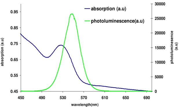
The photoluminesence and the absorption spectrum of nanocrystals with the diameters of 2.4 and 5.2 nm are presented in Fig. 3.3.2 and Fig. 3.3.3
Figure 3.3.2 Absorption and emission spectra of CdSe/ZnS core-shell nanocrystals of 5.2nm in diameter. 1 1.1 1.2 1.3 1.4 1.5 1.6 1.7 1.8 1.9 2 450 490 530 570 610 650 690 wavelength (nm) a b s o rp ti o n ( a .u ) 0 2000 4000 6000 8000 10000 12000 14000 16000 18000 20000 p h o to lu m in e s e n c e ( a .u ) absorption (a.u.) photoluminescence(a.u)
19
Figure 3.3.3 Absorption and emission spectra of CdSe/ZnS core-shell nanocrystals of 2.4 nm in diameter.
These quantum dots absorb the incident light if only the photon energy of the light is larger than effective the gap energy of the quantum dot. This means the band gap of the quantum dots effectively change the application wavelength. The optical emission and the absorption characteristics of the dots are critical for their uses. The narrow photoluminescence curve shows the small size distribution of the quantum dots (in this case ±%5). The absorption of the nanocrystals increase in the UV region of the spectrum. The emission and the absorption curves of the nanocrystals are separated from each, the overlap is very small. This is a critical and beneficial property of the quantum dots since the reabsorption at around the emission wavelength effectively decreases the luminescence of the dots. The luminescence efficiency depends on the quantum efficiency. Quantum efficiency is a parameter for the measure of how much the optical input light can be converted into the optical output light. For the optically
0.45 0.55 0.65 0.75 0.85 0.95 450 490 530 570 610 650 690 wavelength(nm) a b s o rp ti o n ( a .u ) 0 5000 10000 15000 20000 25000 30000 p h o to lu m in e s e n c e ( a .u ) absorption (a.u) photoluminescence(a.u)
20
excited nanocrystals, this is the ratio of the number of the emitted photons to the number of the absorbed ones. So far in the literature, 60% quantum efficiency has been reported for the nanocrystals[60].
For the enhancement of the luminesence of the quantum dots a wider band gap material is used as a shell layer in quantum dots. The wider band gap material on surrounding the core is used to passivate the surface and to confine the excitons to the core to supress the nonradiative recombination of the photogenerated carriers. Due to the better confinement of the carriers, these core/shell nanocrystals have better optical stability and light emission.
Figure 3.3.4 Core shell quantum structure (after [61]).
3.4 Applications of Nanocrystals
Due to the optical properties of the nanocrystals, there is a great ongoing effort on using nanocrystals in device applications. The tunability of their emission and absorption characteristics make them very attractive in the optoelectronis device applications. Some of these applications are LEDs [48-51], photovoltaics [54-58], photodetectors [46-47], optical memories [52] as mentioned before. The narrow emission spectrum of the nanocrystals makes them attractive to be used in light emitting diodes. In LEDs, the electrons and holes into the recombination sites by driving current. At the end, the electron-hole pairs recombine in the nanocrystal and provide spontaneous emission depending on the crystal size. For example, Si LEDs are a good example for the use of the nanocrystals. Although the bulk silicon is an indirect gap material and not
21
suitable for the LED design, the silicon nanocrystals are good candidates for the silicon based LEDs [50].
In the photovoltaic technology the nanocrystals are investigated for the enhancement in the solar cell parameters. These nanoparticles are shown to be promising for the solar conversion efficiency enhancement [55]. Due to the tunable absorptive behavior, nanocrystals are also used for the photodetectors. The work on photodetection mainly is for the enhanced responsivity in the UV and IR regions of the current photodetectors [14, 46-47].
However the applications of the nanocrystals are not limited only to such devices. In biotechnology the quantum dots are being used as the fluorescent tags for the labeling as well.
22
Chapter 4
Nanocrystal Scintillators for
Photodetection
As discussed in the previous chapters, the silicon technology has some limitations for operation in UV. In this chapter we present our research on the development of UV scintillators work on silicon platforms using nanocrystal emitters to enable operation in UV.
4.1 P-N junctions and photodetectors
P-N junctions are one of the most important physical phenomena in optoelectronic device physics. It is formed by interfacing the p- doped and the n-doped materials. These diodes are used as a rectifying element. They pass current through one direction and not in the other direction.
Figure 4.1.1 P-N diode (after [62]).
In the p-n junction, there are a number of physical mechanisms to be discussed. The p region contains excessive holes. On the other side, the n region is abundant with electrons. By the diffusion mechanisms the holes in the p side and the electron in the n side move towards each other. As a result, they leave behind the oppositely charged dopants. For example, while the electrons move through the p-region due to the diffusion mechanism, they leave the positively
23
charged donors behind. The same is true for the holes passing from the p-region to the n-region, leaving negatively charged acceptors. As a result, there is a region created in the middle, the space charge region or the depletion layer. After the formation of the space charge region, there appears an internal electric field because of the space carriers there. This electric field actually opposes to the diffusion of the further motion of the carriers. Thus the build-up of the electric field and the diffusion mechanism continues until they reach an equilibrium and this is the case when no bias is applied to the diode. For the injection and collection of the carriers, one can further apply forward or reverse bias across the end of the diodes.
4.1.1 Forward Bias
A diode is forward biased when its n side is connected to the negative terminal and its p side is connected to the positive terminal of a battery. When forward biased, the carriers in the p-region are pushed through the depletion region and vice versa. As a result, this creates a current passing in the forward direction through the diode. Due to the oppositely charged carrier motion to the opposite sides through the depletion region, the depletion gets thinner and the resistance decreases.
4.1.2 Reverse bias
Connecting the opposite terminals to the diode ends one can apply reverse bias across the diode. In this case the majority carriers in the n-region, which are electrons, are attracted the positive end of the battery, and vice versa. As a result the depletion region broadens and the resistance across the diode increases. Applying more reverse bias than the diode can hold, though, changes the situation. The minority carriers in the p- and n- side (holes for n-region and electrons for p-region) are attracted through the opposite poles of the battery. If
24
voltage more than this threshold is applied across the diode, these carriers flow across the barrier and they ionize the atoms in the crystal. This ionization creates new carriers and the multiplication of these carriers around produces a great amount of current passing and this is called the avalanche breakdown. The avalanche is reasonable as long as the heat produced due to the current does not exceed the limits of the device. If the heating is too much, this may catastrophically damage the diode.
4.1.3 Photodetectors
The operation of the photodetectors relies on the collection of the photocarriers generated in the diode. They are reverse biased in operation and only the photogenerated carriers created in depletion region contribute to the photocurrent unless the carriers created in the p- and n- regions diffuse to the opposite parts. The incident light creates electron and hole pairs in the depletion region and, when the photodiode is reverse biased, the electron and hole pairs are pulled towards the opposite ends of the terminals. This produces photocurrent. In the case where the depletion region is narrow, all of the incident light cannot be absorbed and very little photocurrent is produced. To circumvent this problem, an intrinsic layer is added between the p- and n- regions. The intrinsic region is chosen to be thick enough to absorb all the incident photon light. The diodes in which the intrinsic region is employed as such are called p-i-n diodes (ip-i-nstead of p-p-i-n diodes).
25
4.2 Nanocrystal Scintillators for Photodetection in
UV
Silicon photonics facilitates the ability to realize optoelectronic devices directly on very large-scale integrated electronic circuits [5-6]. This is critically important for optoelectronics to leverage advanced Si fabrication technology (e.g., Si CMOS and SOI) [3, 7] and its high computation power [2, 3]. However, Si material is constrained in different aspects for use in optoelectronics. Such one limitation is observed in Si based photodetectors and cameras that exhibit very poor responsivity in the UV spectral range. Consequently, Si photodetectors fabricated in standard CMOS process and Si CCD cameras cannot be utilized in UV detection and imaging, despite their advanced, low-cost, high-volume processing technologies. On the other hand, there exists a strong demand for UV detection and imaging, for instance in security applications [63, 64]. Here for the first time, we propose and demonstrate nanocrystal based scintillators hybridized on Si platforms to detect and image in the UV with significantly improved responsivity. We describe on the conception, design, fabrication, experimental characterization, and theoretical analysis of CdSe based nanocrystal scintillators hybridized with Si detectors and CCDs.
In this work, we use luminescent CdSe/ZnS nanocrystals hybridized in a host polymer on the Si platform and obtain hybrid Si photodetectors that exhibit highly improved responsivity in the spectral range of 200-240 nm, experimentally with two orders of magnitude peak enhancement with respect to the host polymer film as shown in Fig. 4.2.1.
26
Figure 4.2.1 The spectral ratio of the emitted optical power to the incident power measured on red-emitting nanocrystals at room temperature.
Our nanocrystal based scintillators provide the ability to engineer the optical scintillation properties such as the enhancement spectral range and factor using different nanocrystal types, concentrations, and film thicknesses. Our theoretical modeling and experimental characterization show such nanocrystal integrated Si based hybrid systems hold great promise in UV detection and imaging with their high orders of spectral responsivity improvement and adjustable properties as desired, also presenting market value for commercialization [14].
In our UV scintillators, we utilize nanocrystals for wavelength up-conversion in the processes of photodetection and imaging. There are three fundamental reasons for our choice of nanocrystals in this work: 1.) their high quantum fluorescence efficiency, 2.) their strong absorption, and 3.) the small overlap between their absorption and emission profiles (due to the quantum confinement). For nanocrystals with CdSe as the core and ZnS as the surrounding shell (providing surface passivation), the quantum fluorescence efficiency may increase as high as 60% across the visible spectral range at room temperature [28, 65-66]. Also, the absorption coefficient of such nanocrystals
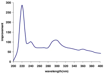
0 50 100 150 200 250 300 200 220 240 260 280 300 320 340 360 380 400 wavelength(nm) im p ro v e m e n t
27
may be very high (ten thousands of cm-1) at short wavelengths, covering the ultraviolet spectral range [28]. These properties make nanocrystals excellent candidates for the scintillator application.
4.2.1 Working principle and design of nanocrystal
scintillators
The working principle of this scintillator relies on the absorption and emission spectra of the nanocrystals that are sufficiently separated from each other. As a result of the high absorption coefficient in the UV region, incident ultraviolet light creates electron-hole pairs with high efficiency, and the resulting recombination occurs at the emission wavelength in the visible range, which is longer than the absorption wavelength. Therefore, by hybridizing nanocrystals, for example, on a Si platform, it is possible to have otherwise undetectable UV photons to be converted to visible photons to be detected by the Si platform. Also, the emission wavelength of the nanocrystals may further be tuned to any desired point in the visible by simply changing the size of the nanocrystals as necessitated by the specification of the scintillator application. For even more efficient performance, the absorption and emission spectra of the nanocrystals may further be separated (e.g., through doping with Mn) to have minimum overlap and thus to minimize reabsorption of the emitted light in principle. In this work, we use conventional core-shell nanocrystals for proof-of-concept device demonstration.
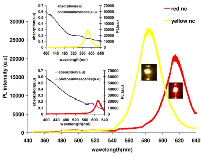
28 0 5000 10000 15000 20000 25000 30000 440 460 480 500 520 540 560 580 600 620 640 wavelength(nm) P L i n te n s it y ( a .u ) red nc yellow nc 0 0.1 0.2 0.3 0.4 0.5 0.6 0.7 400 440 480 520 560 600 640 wavelength(nm) a b s o rp ti o n (a .u ) 0 10000 20000 30000 40000 50000 60000 70000 P L (a .u ) absorption(a.u) photoluminescence(a.u) 0 0.1 0.2 0.3 0.4 0.5 0.6 0.7 400 440 480 520 560 600 640 wavelength(nm) a b s o rp ti o n (a .u ) 0 10000 20000 30000 40000 50000 60000 70000 P L ( a .u ) absorption(a.u) photoluminescence(a.u)
Figure 4.2.1.1 Photoluminescence spectra of our red and yellow nanocrystals (NC). Insets show the absorption spectrum along with the photoluminescence spectrum of the respective nanocrystal.
Figure 4.2.1.1 shows the photoluminescence spectra of our scintillator CdSe/ZnS core-shell nanocrystals when pumped with He-Cd laser at 325 nm at room temperature. The inset shows the photoluminescence and absorption spectra of the respective nanocrystals. The absorption spectrum is obtained using UV-VIS spectrometer. These yellow and red CdSe/ZnS core-shell nanocrystals shown in Fig. 4.2.1.1 are 3.2 nm and 5.2 nm in diameter and exhibit emission peaks at 580 nm and 620 nm, respectively. They have a size distribution of ~5%. They feature quantum efficiencies around 10-20%. Due to the background absorption of host polymer, we typically use an optimal film thickness of 1.5 µm. We design our nanocrystal scintillators using these two nanocrystal types with different concentrations and film thicknesses to investigate and compare the resulting scintillation properties.
29
4.2.2 Characterization of nanocrystal scintillators
The efficiency of our nanocrystal scintillators is determined by the excitation spectroscopy of the nanocrystals. Figure 4.2.2.1 shows the ratio of the emitted optical power to the incident optical power as a function of the excitation wavelength for red type nanocrystals in host polymer. Here we observe that this nanocrystal film is most efficiently pumped between 220 nm and 240 nm. This spectral response implies that the highest enhancement in responsivity is expected to occur in this wavelength range when this nanocrystal film is hybridized on a silicon platform.0 2 4 6 8 10 12 14 16 18 20 200 220 240 260 280 300 320 340 360 380 400 Wavelength (nm) P e m it te d / P i n c id e n t
Figure 4.2.2.1 The spectral ratio of the emitted optical power to the incident power measured on red-emitting nanocrystals at room temperature.
Figure 4.2.2.3 shows the responsivity curves of a silicon detector with and without red nanocrystal hybridization (in red and navy curves, respectively), with the inset of Fig. 4.2.2.3 plotting the improvement in the spectral responsivity with respect to the bare Si detector. Here we observe that the responsivity of the bare silicon detector is improved with the use of nanocrystal scintillator in the entire spectrum except for a dip between 240 nm and 300 nm.
30
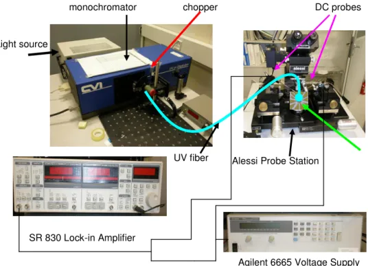
This decrease in the effective responsivity stems from the host polymer that starts absorbing strongly below 300 nm. However, below 240 nm where Si detector exhibits very poor responsivity, the nanocrystals are much more efficiently pumped. Consequently, the effective responsivity is significantly improved between 200-240 nm, despite the increasing absorption level of host polymer. Here using this nanocrystal scintillator, we experimentally achieve effective responsivity in the range of a few milliAmperes/Watts in the spectral range of 200-240 nm. The responsivity measurements are taken using the lock-in amplifier, probe station, voltage supply, Xe light source, monochromator and chopper set-up (Figure 4.2.2.2) in the Class 10,000 characterization lab at Bilkent University Advanced Research Laboratory.
Figure 4.2.2.2 The characterization set-up used in the experiments.
Light source
SR 830 Lock-in Amplifier
Alessi Probe Station
monochromator chopper DC probes
UV fiber
31 0.000 0.005 0.010 0.015 0.020 0.025 0.030 0.035 0.040 200 220 240 260 280 300 320 340 360 380 400 wavelength (nm) re s p o n s iv it y ( A /W ) -100 100 300 500 200 250 300 350 400 wavelength(nm) im p ro v e m e n t( % )
Figure 4.2.2.3 The spectral responsivity of a Si photodetector with and without hybridizing red nanocrystal scintillator measured at room temperature. (The responsivity of bare Si detector is shown in navy curve and that of the same Si detector integrated with red nanocrystal scintillator is shown in red curve; the inset shows improvement of the spectral responsivity.)
Figure 4.2.2.4 characterizes the optical transmission through the red nanocrystal film as well as the host medium of the same thickness, proving strong absorption of the polymer medium. That is why the enhancement of responsivity due to the nanocrystals with respect to the host polymer is much higher, as depicted in Fig. 4.2.1. We experimentally observe that the improvement in the effective spectral response of the red nanocrystal hybridized Si detector is as high as two orders of magnitude around 220 nm in Fig. 4.2.1. This means that the host polymer can be further optimized for this application to achieve high levels of enhancement.
32 0 10 20 30 40 50 60 70 80 90 200 220 240 260 280 300 320 340 360 380 400 wavelength (nm) tr a n s m is s io n ( % ) transmission of polymer transmission of nanocrystals in polymer
Figure 4.2.2.4 Transmission spectra of red nanocrystals and host polymer measured at room temperature.
Figure 4.2.2.5 plots the simulation results of the red nanocrystal scintillator integrated on Si detector, parameterized with respect to the nanocrystal quantum efficiency. Using the semi-empirical data of absorption spectra of the nanocrystals and the host medium, this model simulates the net optical emission from the hybridized nanocrystal film and its effect on the responsivity of the integrating Si detector. As shown in Fig. 4.2.2.5 along with the experimental data, we theoretically expect enhancements in the spectral responsivity as high as three orders of magnitude, one order of magnitude higher than the experimental results, provided that high enough quantum efficiencies are achieved. In this work, the limited quantum efficiency of our nanocrystals reduces the feasible enhancement to two orders of magnitude. This implies that there is much more room for improvement.
33
Figure 4.2.2.5 Semi-empirical simulation results for the improvement in the spectral responsivity of the Si photodetector integrating with red nanocrystal scintillators.
Figure 4.2.2.6 shows the enhancement in the responsivity of the integrating Si detector when hybridized with yellow type nanocrystals this time as another implementation example (in navy curve for bare Si detector and in yellow curve for yellow nanocrystal hybridized Si detector). The yellow nanocrystal scintillator yields enhancement in the responsivity of the integrating Si detector with the same spectral behavior, as in the case of red nanocrystal scintillator shown in Fig. 4.2.2.3 Likewise, the responsivity is improved across the entire spectrum except for the dip in the range of 220-300 nm because of the absorption of the host polymer starting in the UV. However, below 220 nm, where the yellow nanocrystals start to be pumped much more efficiently, the responsivity is improved despite the increasing absorption of the host polymer. Here the yellow nanocrystals lead to improved responsivity at a shorter wavelength in the deep UV range compared to red nanocrystals because of their shifted excitation behavior (due to the size effect).
![Figure 2.1.2.1 Schematic representation of the working principle of a CCD camera (after [20])](https://thumb-eu.123doks.com/thumbv2/9libnet/5913746.122594/20.918.273.710.247.375/figure-schematic-representation-working-principle-ccd-camera.webp)
![Figure 2.1.5.1 Basic p-n photovoltaic device (after [23]).](https://thumb-eu.123doks.com/thumbv2/9libnet/5913746.122594/22.918.333.651.178.364/figure-basic-photovoltaic-device-after.webp)
![Table 2.1.5.1 Reported solar conversion efficiencies of the silicon based photovoltaics (after [27])](https://thumb-eu.123doks.com/thumbv2/9libnet/5913746.122594/23.918.216.748.209.373/table-reported-solar-conversion-efficiencies-silicon-based-photovoltaics.webp)
![Figure 3.3.4 Core shell quantum structure (after [61]).](https://thumb-eu.123doks.com/thumbv2/9libnet/5913746.122594/34.918.347.635.447.583/figure-core-shell-quantum-structure-after.webp)