Laser Writing Deep inside Silicon for 3D Information Processing
O. Tokel1, A. Turnalı2, I. Pavlov1, and F. ¨O. Ilday1,2
1Department of Physics, Bilkent University, 06800 Ankara, Turkey
2Department of Electrical and Electronics Engineering, Bilkent University, Ankara, 06800, Turkey
Micromachining of silicon (Si) with lasers is being investigated since the 1970s [1]. So far, generation of con-trolled subsurface modification in the bulk of Si with high precision has not been achieved. This is highly desirable since successful integration of Si photonics and data transfer elements with conventional Si integrated circuits is proposed to lead to new generations of microprocessors [2,3]. Available techniques fabricate these optical and electronic elements on the top layer of the silion-insulator platform. Despite the remarkable successes of con-ventional techniques, none of the available methods make use of the bulk of Si for positioning functional elements. Here, we report a method for photo-inducing deeply buried (down 1 mm) structures in Si wafers with pulsed in-frared lasers. We demonstrate large aspect-ratio structures with 1-µm widths and long range order over millimetre scales. We further demonstrate multilevel spatial information encoding capabilities in subsurface barcodes.
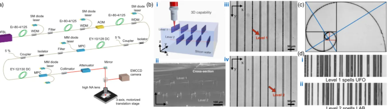
Experimental setup is shown in Fig. 1(a). We incorporated a home-made high pulse-energy, all-fibre-integrated master-oscillator power amplifier (MOPA) system to our processing station. The system can produce 5 ns, 10 W pulses at 100 kHz at 1550 nm. The laser light from the fibre is tightly focused (NA=0.55 or 1.3) onto a Si sample which is intrinsic or doped (n and p type, 1Ω.cm). Experimentally, we found that one of the most critical elements is precise sample alignment with respect to the laser. This is due to the dependence of the physics on counter-propagating beams within the sample volume, interacting in a precise way to create the embedded structures.
Level 1 spells UFO
Level 2 spells LAB
(a) (b)i (c) ii (d) iii iv i ii DFBL high NA lens 3-axis, motorized translation stage EMCCD camera Er-80-4/125 Er-80-4/125 Er-80-4/125 WDM Filter WDM WDM MPC MPC EY-10/128 DC EY-12/130 DC AOM Isolator Coupler Filter Isolator Coupler 5 % 5 % MM diode laser Collimator MM diode laser SM diode laser SM diode laser SM diode laser Attenuator Mirror
Fig. 1 (a) Schematic diagram of the setup. (b) Scheme for Si laser-scribing for multilevel structures. (i) Tight focusing along with optimized pulse energies allow for 3D capability. (ii) Scanning electron microscopy image of multilevel structures. (iii, iv) Infrared (IR) microscopy images confirming the multilevel architecture shown in (ii). (c) Subsurface curved structure, (i.e., golden spiral) written in Si. (d) Multilevel barcodes embedded in Si. Two levels together, decoded with IR microscopy, spell UFOLAB. (i) Level 1 image spelling UFO. (ii) Level 2 image spelling LAB.
We first demonstrate two-level structures written in Si, and later adapt the technique for information encoding in multilevel barcodes embedded in Si. Fig.1(b) shows the production method of multilayered structures. First, the laser was tightly focused with an objective (NA=1.3) to a depth of 80 µm in n-doped (1 Ω.cm) Si, and the sample was raster scanned at this depth which produces Level 1 structures. Then, the focal plane was translated to a depth of 120µm, and to produce the structures at Level 2. The two-level architecture can be directly visualised with scanning electron microscopy (Fig.1b(ii)). IR images of Level 1 and Level 2 structures are given in Fig.1b(iii-iv).We have exploited the rich parameter space provided by the doping, polarisation, scanning speed, and focusing to enable various geometries, including curved structures such as a golden spiral (Fig.1c). As a proof of concept, we adapted this capability to encoding multilevel barcodes in Si. Fig 1d(i) shows reconstruction of a Level 1 barcode, spelling UFO. Fig 1d(ii) shows a barcode embedded deeper than the preceding one, spelling LAB. One is invited to read the barcodes with a QR code reader, which together spell UFOLAB, the acronym for our laboratory. In conclusion, we have developed multilevel architectures embedded in Si with high control and significant potential range of applicability. This new fabrication approach takes advantage of the real estate under the Si surface and therefore can pave the way for creating new electronic devices through electronic-photonic integration. In particular, this new capability can potentially be used for the realisation of multilayered Si chips.
References
[1] I. W. Boyd, “Laser processing of silicon,” Nature303, 481 (1983).
[2] D. Liang, G. Roelkens, R. Baets, and J. E. Bowers, “Hybrid integrated platforms for silicon photonics,” Materials3, 1782 (2010).
[3] E. Kuramochi, et al. “Large-scale integration of wavelength-addressable all-optical memories on a photonic crystal chip,” Nature Photon. 8, 474481 (2014).