OPTOELECTRONICS AND ADVANCED MATERIALS – RAPID COMMUNICATIONS Vol. 4, No. 6, June 2010, p. 859 - 862
Frequency dependent electrical characteristics of
(Ni/Au)/AlGaN/AlN/GaN heterostructures
İ. TAŞÇIOĞLU, H. USLU, Y. ŞAFAK, E. ÖZBAYa
Physics Department, Faculty of Arts and Sciences, Gazi University, 06500, Teknikokullar, Ankara, Turkey
aNanotechnology Research Center, Department of Physics, Bilkent University, 06800 Ankara, Turkey
The main electrical parameters such as ideality factor (n), zero bias barrier height ( Bo), series resistances (Rs), depletion
layer width (WD) and interface state densities (NSS) of (Ni/Au)/AlGaN/AlN/GaN heterostructures have been extracted from
the current-voltage (I-V) at room temperature, and frequency dependent capacitance voltage (C-V) and
conductance-voltage (G/w-V) measurements. The high value of n and Rs were attributed to the existence of an interfacial layer (IL) and
particular distribution of Nss. The density distrubition profile of Nss was obtained from both forward bias I-V data and low-high
frequency (CLF-CHF) measurement methods. In addition, the voltage dependent Rs profile obtained both I-V and admittance
measurements are in good agreement. As a result, the existence of an IL, Rs and Nss lead to deviation from the ideal case
of these heterostructures.
(Received March 01, 2010; accepted June 16, 2010)
Keywords: (Ni/Au)/AlGaN/AlN/GaN, C-V-f and G/w-V-f measurements, Interface states, Rs
1. Introduction
In the ideal case, the C and G/w of metal-insulator-semiconductor (MIS) structures is usually frequency independent but in the applications situation is different especially at low frequencies [1-4]. The interface quality at M/S interface and Rs of device decide the performance and
reliability of these devices. Using a thin film between the metal and semiconductor, such as Si3N4, cannot only
prevent the reaction and inter-diffusion between the metal and AlGaN barrier layer, but can also further improve the retention properties [5,6].In order to determine the Nss,
there are a lot of methodssuch as the I-V [7,8] and CLF
-CHF [1,9] and quasi-static capacitance [10]. Among them,
the I-V and CLF-CHF methods are both simple and
sufficiently reliable. Therefore, in this study, to achieve a better understand the effect of Rs and Nss on main
electrical characteristics, we used I-V, C-V and G/w-V characteristics in the wide frequency range of 2 kHz-2 MHz.
2. Experimental procedure
The (Ni/Au)/AlGaN/AlN/GaN heterostructures were fabricated on (0001) on a double-polished 2-inch diameter (0001), in which sapphire (Al2O3) substrates were grown
in a low pressure Metal - Organic Chemical - Vapor Deposition (MOCVD). Al2O3 substrate was annealed at
1100 °C for 10 min in order to remove surface contamination. The buffer structures consisted of a 15 nm thick, low-temperature (650 °C) AlN nucleation layer, and
high temperature (1150 °C) 420 nm AlN templates. A 1.5 µm nominally undoped GaN layer was grown on an AlN template layer at 1050 °C, followed by a 2 nm thick high temperature AlN (1150 °C) barrier layer. The ohmic contacts were formed as a square van de Pauw shape and the Schottky contacts formed as 1 mm diameter circular dots. Then, Schottky contacts were formed by Ni/Au (40/80 nm) evaporation. The schematic diagram of (Ni-Au)/AlGaN/AlN/GaN heterostructures can be seen in our previous study [11]. The I-V and admittance (C-V and G/w-V) measurements of the (Ni/Au)/AlGaN/AlN/GaN heterostructures were performed using a Keithley 2420 programmable constant current source and an HP4192 A LF impedance analyzer in the frequency range of 2 kHz-2 MHz at room temperature.
3. Results and discussion
The forward and reverse bias I-V characteristics of the
(Ni/Au)/AlGaN/AlN/GaN heterostructures with 40 Å
insulator layer thicknesses (SiNx) were investigated based
on thermionic emission (TE) theory at room temperature. According to TE , the relationship between the I and V through a barrier, with series resistance, is given by [12]
0
2exp Bo exp ( s) 1 exp ( s) (1)
I q q V IR q V IR I AAT kT nkT kT ∗ ⎛ ⎞ ⎛ − ⎞⎡ ⎛− − ⎞⎤ = ⎜− ⎟ ⎜⎝ ⎟⎠⎢⎣− ⎝⎜ ⎟⎠⎥⎦ ⎝ ⎠
Φ
144424443where
Φ
B0 is the zero-bias barrier height, A is the rectifier contact area,A
∗ is the effective Richardson860 İ. Taşçioğlu, H. Uslu, Y. Şafak, E. Özbay
constant and is equal to 32,09 A/cm2K2 for undoped
Al0,22In0,78N [11], in which
I
0 i s the reverse saturationcurrent derived from the straight line intercept of lnI at zero bias voltage. The term IRs is the voltage drop across
the Rs. Fig.1, shows the lnI-V characteristics and it shows a
linear behavior. The values of
I
0and nwere obtained by extrapolating and the slope of linear part of lnI-V plot as 6x10⁻⁶ A and 5.49, respectively.0
B
Φ
value was obtained from the values of I0 and of rectifier contact area as 0,55eV. This high value of n shows that the structures follow an MIS configuration rather than MS SBDs and n can especially be attributed to the existence of an insulator layer, a wide distribution of low BH patches, a tunneling mechanism, and the particular distribution of Nss at the
M/S interface [2,7,8,12,13]. It can be seen from Fig 1, the reverse current increases with the increase of the applied reverse bias and does not go to saturation especially for the reference sample. This lack of saturation for the Schottky contact on an (Ni/Au)/AlGaN/AlN/GaN heterostructure under reverse bias can be explained in terms of the spatial inhomogeneity of BH and the image force lowering in the barrier height [13]. In addition, the voltage dependent Rs
profile was obtained from Ohm’s law (Ri=δVi/δIi) and is
given in Fig1 and it has 203 Ω at 8 V.
Fig. 1. The semi-logarithmic LnI-V characteristics of the (Ni/Au)/AlGaN/GaN heterostructure.
The voltage dependent n and effective barrier height (
Φ
e) can be expressed as [8,12] 0 ( ) ln( / ) qV n V kT I I = (2.a) e e bo Bo d V V dVβ
⎛ Φ ⎞ Φ = Φ + = Φ + ⎜ ⎟ ⎝ ⎠ (2 b)where d
Φ
e/dV is the change in the barrier with biasvoltage. For the MIS type structure, the expression for the Nss as deduced by Card and Rhoderick [8] is reduced as
(
)
⎥ ⎦ ⎤ ⎢ ⎣ ⎡ − − = D s i SS q n W N ε δ ε 1 1 (3)where δ is the thickness of insulator layer, and WD is the
depletion layer width that is being deduced from the C-2-V measurements at 1 MHz. For n-type semiconductor, the energy of interface states Ess with respect to the conductance band edge is given by [21-30-32]
(
)
c ss e
E
−
E
=
q
ϕ
−
V
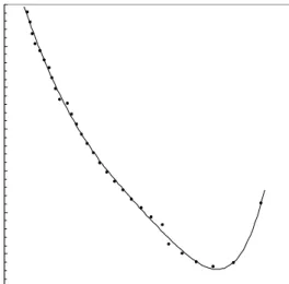
(4) The energy distribution of the Nss for(Ni/Au)/AlGaN/AlN/GaN heterostructures was obtained from the experimental forward bias I-V and is shown in Fig. 2. As can be seen in Fig. 2, the value of Nss is a slight
exponential increase in from the mid-gap towards the bottom of the Ec.
3,0E+13 4,0E+13 5,0E+13 6,0E+13 7,0E+13 8,0E+13 9,0E+13 1,0E+14 0,39 0,41 0,43 0,45 0,47 0,49 0,51 0,53 0,55 Ec-Ess (eV) N ss (e V -1 cm -2 )
Fig. 2. The Nss profile deduced from I-V data of the
(Ni/Au)/AlGaN/GaN heterostructure.
The analysis of the C-V and G/w-V measurements of the high electron mobility transistors (HEMTs) only at one or narrow frequency and bias voltage range can not give us detailed information about conduction mechanisms, barrier formation, Nss. In contrary to, in the wide frequency and
bias voltage region, the C-V and G/w-V measurements of these devices can allow us to understand different aspects of conduction mechanisms. Therefore, the C-V-f and
G/w-V-f characteristics of (Ni/Au)/AlGaN/AlN/GaN
heterostructure have been investigated in the wide frequency range of 2 kHz-2 MHz are given in Fig. 3 (a) and (b), respectively. -12 -11 -10 -9 -8 -7 -6 -5 -4 -3 -8 -6 -4 -2 0 2 4 6 8 10 V (V) L n ( I) (A ) 1,E+02 1,E+03 1,E+04 0 2 4 6 8 V (V) Rs ( Ω )
Frequency dependent electrical characteristics of (Ni/Au)/AlGaN/AlN/GaN heterostructures 861 0,0E+00 5,0E-10 1,0E-09 1,5E-09 2,0E-09 2,5E-09 3,0E-09 3,5E-09 4,0E-09 -22 -18 -14 -10 -6 -2 2 6 10 V(V) C(F ) 20 kHz 30 kHz 50 kHz 70 kHz 100 kHz 200 kHz 300 kHz 500 kHz 700 kHz 1 MHz 2 MHz (a) -1,0E-09 0,0E+00 1,0E-09 2,0E-09 3,0E-09 4,0E-09 -18 -14 -10 -6 -2 2 6 10 V (V) C ( F ) 2 kHz 3 kHz 5 kHz 7 kHz 10 kHz
Fig. 3. The frequency dependent curves of (a) the C-V and (b) G/w-V characteristics of
(Ni/Au)/AlGaN/AlN/GaN heterostructure at room temperature.
As shown in figures, both the C and G/w decrease with increasing frequency. Because, at low frequencies, the Nss can easily follow the ac signal and yield an excess capacitance, which depends on the frequency and time constant of interface states [1,5,14]. The voltage and frequency dependence Rs was obtained from the
measurement capacitance (Cm) and conductance (Gm) at 500, 700 and 1000 kHz [1] and is given in Fig. 4.
2 2 ( ) ma ma ma S C G G R
ω
+ = (5) As shown in Fig. 4, the values of Rs give a peak for each frequency and its magnitude decreases with increasing frequency also the peak position shifts toward the high forward bias region with decreasing frequency. Such behavior of Rs is attributed to interfacial insulator layer (SiNx) and distribution of Nss at M/S interface.The density distribution profile of Nss was also
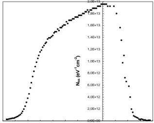
obtained from the low-high frequency capacitance measurements as following eq. [1] and is given in Fig. 5.
1 1 1 1 1 1 ( ) ( ) ss LF i HF i q N A C C C C − − ⎡ ⎤ = ⎢ − − − ⎥ ⎣ ⎦ (6)
where CLF and CHF are the measurement low frequency
capacitance (5kHz) and high frequency capacitance (1 MHz), respectively, and Ci is the insulator layer
capacitance. As shown in Fig 5, the Nss gives a peak and
range from 2.7x10¹¹ to 1.95x10¹³ eV-1cm-2. In addition, the
C-2-V plot at 2 MHz shows a linear behavior, indicates that
the Nss can not follow the ac signal at this high frequency
and consequently do not contribute to appreciably to the structure capacitance. 140 150 160 170 180 190 200 210 -8 -6 -4 -2 0 2 4 6 8 10 12 V (V) R s (Ω ) 500 kHz 700 kHz 1 MHz
Fig. 4. The Rs versus V plots for (Ni/Au)/AlGaN/AlN/GaN
heterostructure. 0,0E+00 2,0E+12 4,0E+12 6,0E+12 8,0E+12 1,0E+13 1,2E+13 1,4E+13 1,6E+13 1,8E+13 2,0E+13 -8 -7 -6 -5 -4 -3 -2 -1 0 1 2 3 4 V (V) Nss (e V -1cm -2)
Fig. 5. The Nss profile deduced from the low-high
frequency C-V data for heterostructure. 0,0E+00 1,0E-08 2,0E-08 3,0E-08 4,0E-08 5,0E-08 -18 -14 -10 -6 -2 2 6 10 V (V) G/ w ( F ) 20 kHz 30 kHz 50 kHz 70 kHz 100 kHz 200 kHz 300 kHz 500 kHz 700 kHz 1 MHz 2 MHz (b) 0,0E+00 1,0E-07 2,0E-07 3,0E-07 4,0E-07 5,0E-07 -18 -14 -10 -6-2 2 6 10 V(V) G/ w ( F ) 2 kHz 3 kHz 5 kHz 7 kHz 10 kHz
862 İ. Taşçioğlu, H. Uslu, Y. Şafak, E. Özbay
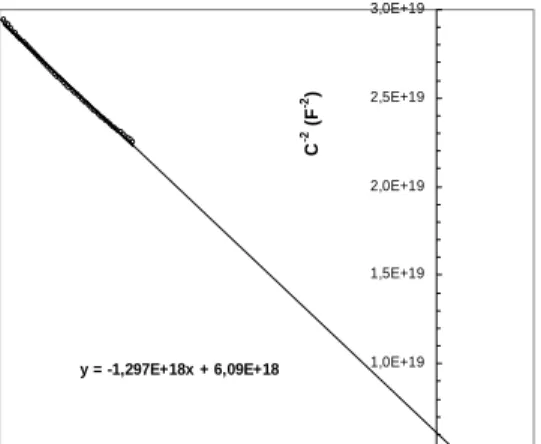
The ND, WD, ΦB and Nss values were obtained from the reverse bias C-2- V plots (Fig. 6) as following equations [10]. B( ) 0 F kT C V V E q Φ − = + + (7) where V0 is the intercept voltage and EF values were
obtained according to, ⎟⎟ ⎠ ⎞ ⎜⎜ ⎝ ⎛ = D C F N N q kT E ln with 2 3 0 * 2 3 15 10 82 . 4 ⎟⎟ ⎠ ⎞ ⎜⎜ ⎝ ⎛ × = m m T N e C (8)
where NC is the effective density of states in conductance band for AlGaN (=3.03x1018 cm-3) and 31
0 9.1 10
−
× =
m kg
the rest mass of the electron. The ND, WD and ΦB values were found as 3.30x1017 cm-3, 3.97x10⁻⁶ cm, 0.96 eV,
respectively y = -1,297E+18x + 6,09E+18 5,0E+18 1,0E+19 1,5E+19 2,0E+19 2,5E+19 3,0E+19 -18 -16 -14 -12 -10 -8 -6 -4 -2 0 2 4 V (V) C -2 (F -2)
Fig. 6. The C-2-V plot for (Ni/Au)/AlGaN/GaN
heterostructure.
4. Conclusions
The (Ni/Au)/AlGaN/AlN/GaN heterostructure with 40 Å interfacial layer (SiNx) was fabricated in order to
investigate the effects of the Nss and Rs on the forward and
reverse bias I-V, C-V, and G/w-V characteristics. The energy density distribution profile of Nss was obtained
from the forward bias I-V measurements by taking into account the bias dependence of the Фe and n(V) of the
devices and the low-high frequency capacitance methods. The high value of n and Rs were attributed to the existence
of an interfacial layer (SiNx) and Nss at M/S interface. In
addition, the voltage dependent Rs profile obtained both
I-V and admittance measurements are in good agreement. In conclusion that the existence of interface layer (IL), Rs and
Nss lead to deviation from the ideal case of these
heterostructures.
References
[1] E. H. Nicollian, J. R. Brews, Metal Oxide
Semiconductor (MOS) Physics and Tchnology, John Willey & Sons, New York, 1982.
[2] Ş. Altındal, H.Kanbur, İ. Yücedağ, A. Tataroğlu, Microelectron. Engin. 85, 1495 (2008).
[3] J. Werner, A. F. J. Levi, R. T. Tung, M. Anzlowar, M. Pinto, Phys. Rev. Lett. 60, 53 (1988).
[4] P. Chattopadhyay, B. Raychaudhuri, Solid State Electron. 35, 605 (1993).
[5] S. Zeyrek, Ş. Altındal, H. Yüzer, M. M. Bülbül, Microelectron. Eng. 83, 577 (2006).
[6] B. R. Chakraborty, N. Dilawar, S. Pal, D. N. Bose, Thin Sol. Films 411, 240 (2002).
[7] O. Pakma, N. Serin, T. Serin, Ş. Altındal, Semicond. Sci. Technol. 23, 105014 (2008).
[8] H.C. Card, E.H. Rhoderick. J Phys D: Appl Phys. 4, 1589 (1971).
[9] R. Castagne, A. Vapaille, Surface Science 28(1), 157 (1971).
[10] M. Kuhn, Solid State Electron. 13(6), 873 (1970). [11] E. Arslan, Ş.Altındal, S. Özçelik, E. Özbay, J. Appl.
Phys. 105, 023705 (2009).
[12] S. M. Sze, Physics Semiconductor Devices, John Wiley and Sons, New York, 1981.
[13] J. P. Sullivan, R. T. Tung, M. R. Pinto, W. R. Graham, J. Appl. Phys. 70, 7403 (1991).
[14] O. Pakma, N. Serin, T. Serin, Ş. Altındal, J. Phys.D: Appl. Phys. 41, 215103 (2008).
_______________________