PHOTONIC CRYSTALS AND MICROSTRUCTURES
Experimental investigation
of layer-by-layer metallic
photonic crystals
B. Te m e I ku ran
H.Altug E.Ozbay
Iiuikxing terms: Photonic crystals. Defect structures, Millimetre wuves, Resonant detectors
Abstract: The authors have investigated the transmission properties and defect characteristics of layer-by-layer metallic photonic crystals. Thay have demonstrated experimentally that the metallicity gap of these crystals extends to an upper band-edge frequency, and no lower edge was detected down to 2GHz. The defect structures built around these crystals exhibited high transmission peak amplitudes (1 00%) and high Q factors (2250). The crystals with low filling ratios (around 1-2%) were tested and were still found to possess metallic photonic crystal properties. These crystals exhibited high reflection rates within the metallicity gap and reasonable
defect mode characteristics. A power
enhancement factor of 190 was measured for the electromagnetic (EM) wave within planar cavity structures, by placing a monopole antenna inside the defect volume. These measurements show that detectors embedded inside a metallic photonic crystal can be used as frequency selective resonant cavity enhanced (RCE) detectors with increased sensitivity and efficiency when compared to conventional detectors.
1 Introduction
Photonic crystals are periodic structures having the property of reflecting the EM waves in all directions for a certain range of frequencies [l-61. Earlier investi- gations were mainly concentrated
on
dielectric based photonic crystals, and were successful in various appli- cations [7-101 but some of their properties restrict the wide usage of these materials. First, dielectric based photonic crystals have low rejection rates per layer, so a large number of layers are needed for applications requiring high isolation purposes [ l 11. Second, for applications around the 1-1OGHz range, these crystals become impractical due to their relatively large dimen- sions. As an exaniple, for a 2GHz application, the die- lectric based photonic crystal will have a typical size of 100 x 100 x 20cm, which will be an important limiting 0 IEE, 1998IEE Proceedings online no. 19982471
Paper first received 25th June 1998 and in revised form 18th November 1998
The authors are with the Department of Physics, Bilkent University, Bilkent, Ankara, 06533 Turkey
factor for many applications. These problems can be solved by introducing metals to photonic crystals [ 12-2 I].
a
b
Fig. 1
a fct; h st based crystals
Schematic diugrams of,fit and st busedphotonic crystals
2 Crystal structure
In this paper, we have investigated the properties of two types of layer-by-layer metallic photonic crystals. The first structure, in which the stacking sequence repeats every four layers, is the equivalent of
a
face centred tetragonal (fct) lattice as shown in Fig. la. Fig. lb shows the other structure similar to the first, but with a repeating sequence of two layers, which is the analogue of a simple tetragonal (st) lattice. The metallic rods used in these crystals were 0.8mm wide, 2.5mm thick and 120mm long, and were placed with a centre to centre separation of 7.6mm. The rods were obtained by machining 150 x 150 x 5mm aluminium blocks. These blocks were then stacked together to form either fct or st structures depicted in Fig. 1. 3crystals
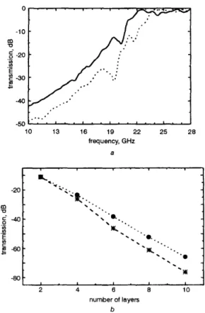
We first measured the transmission properties of both structures using a Hewlett-Packard 85 1OC network analyser, and standard-gain microwave antennas. Fig. 2a compares the transmission properties of 6-layer Transmission properties of metallic photonic
409 IEE Pros-Optoelectron , Vol 145, No 6 , December 1998
fct and st based crystal structures where the propaga- tion direction of the EM wave is along the stacking direction. Both crystals yielded bandgaps with upper edges
-
2OGHz, and no lower edge exists down to 10 GHz. Fig. 2a shows the rejection ratios for two differ- ent crystal structures at 12GHz, as the number of lay- ers are increased. The typical rejection factors of 7-8dB per layer are observed at IOGHz, which is significantly superior to dielectric-based photonic crystals having a maximum rejection of 3-4dB per layer at midgap fre- quencies. -10 m U $ -20 ._ U) ._ E e -30 c -40 -50 10 13 16 19 22 25 28 frequency, GHz a -~ 2 4 6 8 10 number of layers bFig. 2 Trcinvnission cliuructeristics of 6-luver f i t and .st bused metallic pliotonie cry.stcif.s, und cIiunge in rejectioii ruitJs i j these crystul stmcturtv
us numhiv of I u y m i s increuxd
U fct ~~ st: h -. s t - -* - fct
-10
-
._
.
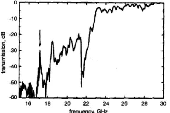
The metals are peffect reflectors at microwave fre- quencies, and EM waves cannot penetrate into these materials. This property results in the metallicity gap which is expected to extend down to OGHz [19]. In
order to verify this, we measured the transmission properties of a 10-layer st based metallic crystal using two monopole antennas, instead of standard gain horn antennas. The monopole antennas, which were con- structed by removing the shield around one end of a microwave coaxial cable, were used to transmit and receive the EM wave radiation. As seen in Fig. 3, the bandgap still exists even at frequencies as low as 2GHz. Since the monopole antenna radiates in all directions, these measurements also reveal the fact that the metallicity gap conserves its property of reflecting the EM wave in all directions. The relatively low rejec- tion ratio observed, which is still higher than its dielec- tric equivalent, is mainly due to the following two reasons: first, the finite size of our crystal compared to large wavelengths at which the measurement is made was a limiting factor. Secondly, the radiation efficien- cies of the monopole antennas used were relatively poor.
As we mentioned earlier, if dielectric materials were used, the crystal dimensions will be in the metre scale in order to have a bandgap at 2GHz. The dimensions of the metallic crystal we investigated, which is suitable for applications at these frequencies, is about an order of magnitude smaller than its dielectric counterpart. The three orders of magnitude reduction in the struc- ture volume makes the usage of metallic photonic crys- tals feasible for low frequency applications.
4 Defect structures in metallic photonic crystals
It was previously shown in dielectric based layer-by- layer photonic crystals that defect structures around this geometry can be built by means of adding or
-70
-60i
10 13 16 19 22 25 frequency, GHz a -40 17.16 17.18 17.20 17.22 frequency, GHz bFig. 4 Trunsmi.s.sion c11ciructcri.stics of’ ICluyer s t bused crystul ~ , i t h u
single rod rernovcd def2c.t structure, und expunntled ,frequency .sc~cile of U
removing rods from an otherwise perfect crystal [l 11. The same idea was used to investigate the defect char- acteristics of these metallic photonic crystals 1121. Fig. 4a shows the transmission properties of 14-layer st type photonic crystals where $he 7th layer is the defect layer with a single missing rod. The defect mode was only observed when the electric field polarisation vector of the incident EM wave e was parallel to the rods of the defect layer. The defect mode was observed at 17.2GHz with a peak transmission amplitude of -7d3, and a Q factor (quality factor, defined as the centre fre- quency divided by the peak’s full width at half maxi- mum) of 750. Increasing the number of layers to 18 (where the 9th layer was chosen as the defect layer) yielded a defect mode with an increased Q factor of 1740 and a peak transmission of -19dB (Fig. 4b).
-1 O0 b
16 18 20 22 24 26 28 30
frequency, GHz Fig. 5
gle rod removed defect structure
Defect characteristics of a 14-layer f i t based crystal with a sin-
B
‘EE
e C .- U)-
B
.s 0 7 10 13 16 19 22 25 28 frequency, GHz B 0 200 400 600 800 lo00 1200 inverse transmission () l b 1Fi .6 Transmission characteristics of 8-layer st based photonic cr stal w i x no gap (solid line), and with planar dejects with separation wid& of ( i ) 3mm, (ii) Smm, (iii) 7mm, (iv) 9mm, (v) I l m m , (vi) 14mm and
( v i ) 15.5mm (dotted lines), and chmge in Q factor of de ect modes as a
,+ction of inverse mirror transmission of cavity at defect jLquency
A similar defect structure built around fct based pho- tonic crystal gave a higher Q factor of 950, but with a low peak transmission amplitude of -30dB (Fig. 5). This put a limit to achieve a higher Q factor by increas- ing the number of layers, where the peak transmission dropped below the noise level. In the following investi- gations, we concentrated on st based metallic photonic crystals, which are superior to fct based photonic crys- tals considering the advantages of the higher peak amplitude and maximum achievable Q factors.
We then investigated the planar type of defect struc- tures, built around an 8-layer st based photonic crystal. The planar defect was obtained by separating the 4th and 5th layers of the crystal. This resulted in a planar airgap between the two photonic mirrors, each formed of a 4-layer (2-unit cell) crystal. Fig. 6a shows the transmitted EM wave, along the stacking direction, through the planar defect structure with separation widths of 3, 5 , 7, 9, 11, 14 and 15.5mm (with corre-
sponding labels 1, 2, 3, 4, 5, 6 and 7, dotted lines), and with no gap (solid line). Although the transmitted peak amplitude drops from 100% transmission at 17 GHz to -1 1.3dB at 7.4GHz, there exists a significant increase in the Q factor from 115 to 1450. Both of these obser- vations can be explained by considering our structure as a Fabry-Perot cavity. The increase in the reflectivi- ties of the mirrors of a Fabry-Perot cavity results in a lower transmitted peak amplitude and a higher Q fac- tor [22]. In order to see this effect, we plotted the Q factors of the defect modes as a function of inverse transmission of the mirrors (4-layer crystal) of the cav- ity at the corresponding defect frequency (Fig. 6b). The curve is expected to be linear if the mirrors of the cav- ity were large compared to the resonant wavelength of the cavity [22]. As the resonant wavelength and the cavity width increases, due to the finite size of our crys- tal mirrors, the curve deviates from linearity and flat- tens. These results show that this structure can be used to create defect modes with high Q factors at frequen- cies as low as a few GHz, which is nearly impossible for dielectric based photonic crystals.
10.605 10.610 10.615 10.620
frequency, GHz
Transmission characteristics of a planar &feet mode with a Q Fig. 7
factor of 2250, in an expanded frequency scale
Another way to increase the Q factors of these planar defect structures is to increase the rejection ratio of photonic mirrors of the cavity by increasing the number of layers. As shown in Fig. 7, a 12-layer phot- onic crystal separated from the middle with a separa- tion width of lOmm resulted in a Q factor of 2250, with a peak transmission amplitude of -25dB at
1 0.6 GHz.
41 I
We continued to explore the properties of the planar defects in metallic structures by changing the angle of incidence of the EM wave. Increasing the angle of inci- dence, peaks other than the main peak at 8 = 0" (where
8 is the angle between the surface normal of the crystal and the incident EM wave) came into view. If we con- tinue to increase the angle further, we observe that a number of peaks appearing at higher frequencies domi- nate. while the peak transmission amplitudes of lower
??
'E
e
e i .- U) c m i U .- In U) .-6
e c%
c' ._ U) .-E
e cB
e- Ee
e ._ U) ._ L 0 . , . , . , .1
-20-
-40-
-60 a b C 10 12 14 16 18 20 22 24 frequency, GHz dFi 8 Additional defict n?ode.s observed f o r planar defect structures wi%incrcwsii,:g angle qf incidence
412
frequency modes diminish, disappearing at the noise level. The frequencies of the defect modes do not shift with the changing angle of incidence, but dominate at
certain fixed frequencies for certain angles. These observations are demonstrated in Fig. 8, where the angle of incidence is changed from 0" to 50°, measured from a 12-layer photonic crystal separated from the
middle by a 5mm gap. These defects cannot be
explained by a simple Fabry-Perot model [ l l , 131, since the next resonance is around 7-8GHz away from the observed one, while the consecutive peaks appear with a separation < 1GHz. An explanation can be made using the theory of resonant cavities, where the reflect- ing mirrors are considered to be curved. The solution for this structure is a combination of Hermite Polyno- mials, which results in additional peaks other than the main resonance. This unexpected phenomenon is under further theoretical and experimental investigation.
frequency, GHz a 200 t I 14.8 15.0 15.2 15.4 frequency, GHz b Fig. 9
8-liiyvr si Enhancement cliaructeristics bused meiullic plioionic crystal
of' a planar defict structure within
5 Resonant cavity enhancement
The electric fields in cavities are usually enhanced, and by placing active devices in such cavities, one can make the device benefit from the wavelength selectivity and the large enhancement of the resonant EM field within the cavity [22]. This effect has already been used to achieve novel devices such as resonant cavity enhanced (RCE) photodetectors and light emitting diodes [23, 241. In order to demonstrate this effect, we placed a monopole antenna inside the defect volume of planar defect structures described above. We used the network analyser and the standard gain horn to obtain EM waves, and the monopole antenna, which is also con- nected to the network analyser, as a receiver. The sin- IEE Pioc -0ptoelectioii V d 145 N o 6 Deien?her 1998
gle pass absorption data of the probe was used to calibrate the meamred enhancements.
Our previous investigations on dielectric photonic crystals show that asymmetric planar cavities result in higher enhancement factors when compared to sym- metric ones [25]. Fig. 9 shows the enhancement charac- teristics of a planar type of defect structure, with a 4- layer thick front mirror and a 6-layer thick back mir- ror. At a 5mm Separation width of the cavity, the defect frequency was observed to be at 15.08GHz. We observed a power enhancement factor of 190 at the defect frequency, with a Q factor of 335. When com- pared with enhancement factors obtained in cavity structures built around dielectric photonic crystals, this value is rather small. This may be the result of small but finite absorption coefficients of metals, which exist even at microwave frequencies. This absorption becomes significant when we consider the high number of times the field circulates inside the cavity and experi- ences a loss in each cycle. Still these investigations sug- gest the possibility of using an embedded detector inside a metallic photonic crystal, as a frequency selec- tive RCE detector with an increased sensitivity and effi- ciency. As an example, detectors based on photonic crystals will be more efficient than a typical frequency selective LC resonant circuit detector as the EM field does not recycle in such detectors. The RCE detectors based on photonic crystals are also superior to other types of resonant cavity antennas such as patch anten- nas. The ultra-high EM wave rejection properties of photonic crystals result in better and more controlled confinement of the resonant EM field in all directions. This means photonic crystal based RCE detectors will have higher quality factors and better frequency selec- tive properties when compared to conventional RCE detectors.
6 Towards lower filling ratios
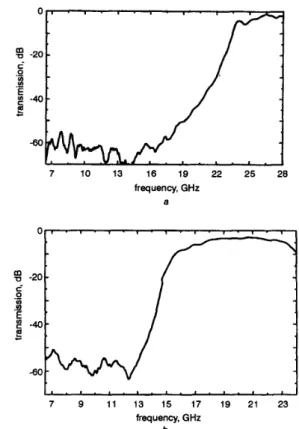
Although the filling ratio of the metallic crystal we have investigated has quite
a
lower filling ratio (1 1%) when compared with its dielectric equivalent (30%), considering the high rejection ratio property of metals, it is possible to lower the filling ratio further. There- fore, we constructed and tested a new layer-by-layer structure, with cylindrical metallic rods which are 0.7mm in radius, 150mm long, and with centre to cen- tre separation of 6mm. The rods of the consecutive lay- ers are placed perpendicular to each other, along the stacking direction, and are touching in couples. These touching couples of layers form a square mesh surface, and are separated from each other by 6mm in st and 3mm in fct based crystals. This structure results in a filling ratio of 1.1% in st and 2.2% in fct crystals.Fig. 10 shows the transmission properties of 7-mesh layer fct (a) and st (6) based photonic crystals. The upper band-edge is at 24GHz in fct based crystal, and shifts to 15GHz in st based crystal. The metallicity gap extends to lower frequencies as expected. The average rejection rate per mesh layer
of
these crystals is-
8-lOdB, which is superior to that of the dielectric based photonic crystals.
Defects created by removing rods in this structure resulted in similar defect modes observed in other pho- tonic crystals, but with lower peak transmission ampli- tudes and lower Q factors. Fig. 11 shows the transmission properties of a 7-mesh layer fct (a) and st
(b) based crystals with a defect introduced by removing
IEE Proc -0ptoelectrun. Vol 145, Nu 6, December 1998
7 10 13 16 19 22 25 28 frequency, GHz a 7 9 11 13 15 17 19 21 23 frequency, GHz b Fig. 10
layer-by-layer metallic photonic crystals a fct; b st based crystals
Transmission properties of low filling ratio f c t and st bused
8 10 12 14 16 18 20 22 24 26 28 frequency, GHz a 8 10 12 14 16 18 20 frequency, GHz b Fig. 11
low filling ratio photonic crystals a fct; b st based crystals
Clzaracteristics defect structures built uround f c t and st based
a single rod from the 4th layer. This time, contradic- tory to the other type of crystal, fct based crystal is superior to st based one considering the higher peak transmission amplitudes (-1 1.2dB in fct and -18.4dB in st) along with the same Q factors (150 in both). The relatively poor defect characteristics of st based crystals may be assigned to the leakage of the EM waves from the sides of the separation planes of the consecutive touching couples of layers, which is lower (but still sig- nificant) in fct based crystals.
These results, although not as good as the previous type of crystal, are of great importance considering applications which require crystals that are light and that have low filling ratios. Also, since metals exhibit high absorption at optical frequencies, these crystals with their minimised metal contents, when compared to the other metallic crystals we investigated. will be quite useful at optical frequencies if built in sufficiently small dimensions.
7 Conclusion
We have investigated the properties of metallic layer- by-layer photonic crystals. An average rejection rate of 8dB per layer was measured. We have observed that the metallicity gap extends down to frequencies as low as 2GHz without any lower band-edge. Defect modes created by removing rods resulted in high peak trans- mission (80%) and high Q factors (1740). Planar type defect structures exhibited loo‘% peak transmission amplitudes. and higher Q factors (2250), and existed at low frequency values (- 7GHz). We also demonstrated the RCE effect in planar cavities built around metallic photonic crystals. A new type of crystal with very low filling ratio is tested and the existence of the metallicity gap and the defect modes were observed. With all these advantages, metallic photonic crystals are suitable for various applications at microwave, millimetre wave and submillimetre wave frequencies. Considering the second type of crystal (with low filling ratio), these applica- tions may also be extended to optical frequencies.
8 Acknowledgments
This work is supported by the Turkish Scientific and Technical Research Council of Turkey (TUB I TAK) under contract 197-E044, NATO Grant SfP971970, National Science Foundation Grant INT-95 128 12 and NATO-Collaborative Research Grant 950079.
9 References
1 HO, K.M., CHAN, C.T., and SOUKOULIS, C.M.: ‘Existence of
a photonic gap in periodic dielectric structures’, Phys. Rev. Lett.,
2 YABLONOVITCH, E., GMITTER, T.J., and LEUNG, K.M.: ‘Photonic band structure: the face-centered-cubic case employing nonspherical atoms’, Phys. Rev. Lett., 1991, 67. (17), pp. 2295- 2298
JOHN, S.: ‘Strong localization of photons in certain disordered dielectric superlattices’, Phy.~. Rev. L e f t . , 1987, 58, (23), pp. 2 4 8 6 2489
1990, 65, (25), pp. 3152-3155
3
4 SOUKOULIS, C.M. (Ed.): ‘Photonic band gap materials’ (Plc- num, New York. 1996)
‘Photonic crystals: putting a twist on light’, Nciture. 1997, 386, pp. 143-149
6 KRAUSS, T.F., D E LA RUE, R.M., and BRAND, S . : ‘Two- dimensional photonic-band gap structures operating at ncar-infra- red wavelengths’, Nuture, 1996. 283, pp. 699-702
OZBAY, E.: ‘Layer-by-layer photonic crystals I‘rom microwave to far infrared frequencies’, J . Opt. Soc. An?. B. 1996. 13, (9). pp. 1945-1 955
WANKE, M.C., LEHMANN, O., MULLER, K.. WEN, Q.. and STUKE, M.: ‘Laser rapid prototyping of photonic band-gap microstructures’, Science, 1997, 275, (5304). pp. 1284-1280 9 HO, K.M.. CHAN, C.T., S O U K 0 U L I S. C . M . . BISWAS? R.,
and SIGALAS, M.: ‘Photonic bandgaps in three dimensions: New layer-by-layer periodic structures’. Solid Stcite C‘onnnun., 1994, 89, ( 5 ) , pp. 413416
10 KRAUSS, T.F., VOGELE, B.. STANLEY, C.R., and DE LA RUE, M.: ‘Waveguidc microcavity based on photonic microstruc- tures’, IEEE Pliotonics. Techno/. Lrtt.. 1997, 9, ( 2 ) , pp. 176-178 1 1 OZBAY, E., and TEMELKURAN, B.: ‘Retlection properties
and defect formation in photonic crystals’. Appl. P/7j.s. Lett., 1996, 69, ( 6 ) , pp. 743-745
12 OZBAY, E., TEMELKURAN, B., SIGALAS, M.. TUTTLE, G., SOUKOULIS, C.M., and HO, K.M.: ‘Defect structures in metallic photonic crystals’, App/. Ph,vs. Lett., 1996. 69, ( 2 5 ) . pp. 3797-3799
13 TEMELKURAN. B., OZBAY. E., SIGALAS. M.. TUTTLE, G., SOUKOULIS, C.M., and HO, K.M.: ‘Reflection properties of metallic photonic crystals’, Appl. Phys. A , 1998, 66. pp. 363- 365
14 JOANNOPOULOS, J.D., MEADE. R.D., and WINN. J.N.: ‘Photonic crystals’ (Princeton University Press. 1995)
5 JOANNOPOULOS, J.D.. VILLENEUVE, P.R.. iii~d F A N , S . :
7
8
15 SIEVENPIPER, D.F.. YABLONOV~TCH, E., W I N N , J.N.,
FAN, S., VILLENEIJVE. P.R., and JOANNOPOULOS, J,.D.: ‘3D metallo-dielectric Dhotonic crystals with strong cimacitive coupling between melahic islands’; Phys. Rev. Let;. 1498, 80, (13), pp. 2829-2832
16 GUPTA, S . , TUTTLE, G., SIGALAS. M., and HO, K.M.: ‘Infrared filters using metallic photonic bandgap structures on flexible Substrates’, Appl. Phys. Lf’tt., 1997, 71, (17), pp. 2412- 2414
17 KUZMIAK, V., and MARADUDIN, A.A.: ‘Photonic structures of one- and two-dimensional periodic systems with metallic com- ponents in the presence of dissipation’, Plzys. Rev. B, 1997, 55. (12), pp. 7427-7444
18 SCALORA, M., BLOEMER, M.J., PETHEL, A S . . DOWLING.
J.P., BOWDEN, M., and MANKA, A.S.: ‘Transparent, metallo- dielectric, one dimensiomal, photonic band-gap structures’, J . 19 SIEVENPIPER, D.F., SICKMILLER, M.E., and YABLONO- VITCH, E.: ‘3D wire mesh photonic crystals’, P / J ~ s . Rcv. Lett.,
1996, 76, (l4), pp. 2480-2483
Appl. P h ~ s . , 2377-2383, 1998, (83), pp. 5
20 MCINTOSH, K.A., MAHONEY, L.J., MOLVAR, K.M., MCMAHON, O.B., VERGHESE, S., ROTHSCHILD. M., and BROWN, E.R.: ‘Three-dimensional metallodielectric photonic crystals exhibiting resonant infrared stop bands’, Appl. P1iy.s.
Lett., 1997. 70, (22), ~ p . 2937-2939
21 SIGALAS, M.M., CHAN, C.T., HO, K.M., and SOUK- OULIS, C.M.: ‘Metallic photonic band-gap materials’, Phys. Rro.
B, 1995, 52, (16). pp. 11744-11751
22 SIEGMAN. A.E.: ‘Lasers’ (University Science Books, Mill Val- ley, 1986)
23 UNLU, M.S., GOKKAVAS, M., ONAT, B.M., ATA, E.. OZBAY, E., MIRIN, R.P., KNOPP, K.J., and CHRIS- TENSEN, D.H.: ‘High bandwidth-efficiency resonant cavity enhanced Schottky photodiodes for 800-850nm wavelcngth oper- ation’, Appl. Phys. Lett., 1998, 72, (2). pp. 2727-2729
24 OZBAY. E., ISLAM, M.S.. ONAT, B., GOKKAVAS. M..
AYTUR, O., TUTTLE, G., TOWE, E., HENDERSON, R.H., and UNLU, M.S.: ‘Fabrication of high-speed resonant cavity enhanced Schottky photodiodes’, IEEE Photonics. Tecllnol. Lett.,
1997, 9, (5), pp. 672-674
25 TEMELKURAN, B.. OZBAY, E., KAVANAUGH, J . P . , TUT- TLE. G.. and HO. K.M.: ‘Resonant cavitv enhanced detectors embedded in photonic crystals’, Appl. Plzys.’ Lett., 1998, 72, (19). pp. 2376-2378