GRATING BASED PLASMONIC CAVITIES
a thesis
submitted to the department of physics
and the institute of engineering and science
of bilkent university
in partial fulfillment of the requirements
for the degree of
master of science
By
Servet Se¸ckin S¸enlik
July, 2009
Prof. Dr. Atilla Aydınlı (Advisor)
I certify that I have read this thesis and that in my opinion it is fully adequate, in scope and in quality, as a thesis for the degree of Master of Science.
Assoc. Prof. Dr. O˜guz G¨ulseren
I certify that I have read this thesis and that in my opinion it is fully adequate, in scope and in quality, as a thesis for the degree of Master of Science.
Prof. Dr. ¨Omer Da˜g
Approved for the Institute of Engineering and Science:
Prof. Dr. Mehmet B. Baray Director of the Institute
ABSTRACT
GRATING BASED PLASMONIC CAVITIES
Servet Se¸ckin S¸enlik M.S. in Physics
Supervisor: Prof. Dr. Atilla Aydınlı July, 2009
Surface plasmon polaritons are dipole carrying electromagnetic excitations occur-ing at metal-dielectric interfaces. Metallic periodic structures exhibit modified transmission and reflection spectra owing to the interaction of propagating SPPs with the periodicity. These periodic surfaces are used to demonstrate localiza-tion of propagating SPPs. Thin metallic films surrounded by Bragg reflectors, selective loading of biharmonic metallic surfaces and Moire patterns are used to demonstrate plasmonic cavity formation. The quality factor, Q, a characteristic value that indicates rate of energy loss relative to the stored energy in the cavity is a crucial parameter for classifying these cavities. It was proposed that the Q factor should strongly depend on the surface geometry. However, there was not a sytematic study on the Q factor of these cavity structures. In this work, we report on a comparative study of grating based plasmonic band gap cavities. Numerically, we calculate the quality factors of the cavities based on three types of grating surfaces; uniform, biharmonic and Moir`e surfaces. Experimentally, we demonstrate the existence of plasmonic cavities based on uniform gratings. Effective index perturbation and cavity geometries are obtained by additional dielectric loading. Furthermore, we fabricate 2D plasmonic structures, observe plasmonic band gaps in the symetry axis and propose cavity geometries for this structure.
Keywords: Surface plasmon polaritons, Localization, Biharmonic gratings,
Uni-form gratings, Moir`e surface, Cavity, Quality factor.
KIRINIM A ˜
GI TABANLI PLAZMON˙IK KOVUKLAR
Servet Se¸ckin S¸enlik Fizik B¨ol¨um¨u, Y¨uksek Lisans Tez Y¨oneticisi: Prof. Dr. Atilla Aydınlı
Temmuz, 2009
Y¨uzey plazmon polaritonları, metal-dielektrik y¨uzeylerinde hareket eden ¸ciftkutup ta¸sıyan elektromanyetik hareketlenmelerdir. Metalik periyodik y¨uzeyler hareket eden y¨uzey plazmon polaritonları ile etkile¸serek o y¨uzeylerin ge¸cirgenlik ve yansıtma ¨ozelliklerini de˜gi¸stirir. Bu periyodik y¨uzeyler hareket eden y¨uzey plazmon polaritonların yerelle¸stirilmesinde kullanılmaktadırlar. Bragg yansıtıcıları tarafından ¸cevrelenmi¸s ince metal kaplamalar, ¸cift periyotlu me-talik kırınım a˜glarının tercihli kaplanması ve Moire y¨uzeyleri plazmonik kovuk-ların g¨osterilmesinde kullanılmı¸stır. Kalite fakt¨or¨u kovuklardaki enerji kaybının depolanan enerjiye oranıdır ve plazmonik kovukları sınıflandırmada ¨onemli bir ¨ozelliktir. Kalite fakt¨or¨un¨un y¨uzey geometrisine ba˜glılı˜gı ¨one s¨ur¨ulm¨u¸s ama sis-tematik bir ¸calı¸sma yapılmamı¸stır. Bu tezde kırınım a˜gı tabanlı plazmonik kovuk-ların kalite fakt¨orlerine ili¸skin bir ¸calı¸sma yapılmı¸stır. Sayısal olarak, tek peri-yotlu, ¸cift periyotlu kırınım a˜gları ve Moire y¨uzeylerindeki plazmonik kovukların kalite fakt¨orleri hesaplanmı¸stır. Deneysel olarak, tek periyotlu kırınım a˜gları ¨ust¨unde plazmonik kovuk olu¸sumu g¨osterilmi¸stir. Ayrıca, iki boyutlu plazmonik bant aralı˜gı yapıları ¨uretilmi¸stir ve bu yapılar i¸cin kovuk geometrisi ¨onerilmi¸stir.
Anahtar s¨ozc¨ukler : Y¨uzey plazmon polaritonları, Yerle¸sme, C¸ ift periyotlu kırınım a˜gları, Tek periyotlu kırınım a˜gları, Moire y¨uzeyleri, Kovuk, Kalite fakt¨or¨u.
Acknowledgement
I would like to express my indebtedness to my academic supervisor Prof. Atilla Aydınlı for his encouragement and guidance.
I would like to thank Dr. A¸skın Kocaba¸s for introducing me surface plasmons and teaching his experience in laboratory.
I would also like to thank my thesis committe, Prof. ¨Omer Da˜g and Prof. O˜guz G¨ulseren for their reading and commenting on this thesis.
I would like to thank my group mates Samed Yumruk¸cu, Ertu˜grul Karademir and Mustafa Karabıyık for valuable discussions and their friendships. I would like to thank to Ertu˜grul once more for his technical support and I would also like to thank Dr. Mecit Yaman for his critical reading of this work.
I would like to thank Ahmet Kele¸s for his sincere friendship and especially his motivation talks. I would like to thank H. Esat Kondak¸cı for his friendship and support.
I am indepted to Tuncay ¨Ozel and Samed Yumruk¸cu (a.k.a 2+1) for their friend-ships and support during my seven years in Bilkent. Their support is invaluable for me.
I wish to express my attidues to Mustafa ˙Incebacak (a.k.a Musti) for his endless friendship and ˙Incebacak family for their support (F2-49).
I wish to express my special thanks to my parents, my elder brother Niyazi and my aunt for their support and love.
I wish to express my deepest graditudes to my wife, ¨Ozlem for always being near myself. Without her support, encouragment and love, this work would be impos-sible.
The financial support from Turkish Scientific and Technical Research Council (TUBITAK) is also gratefully acknowledged.
Contents
1 Introduction 1
2 Fundamentals of Surface Plasmon Polaritons 3
2.1 Optical Properties of Metals . . . 3
2.1.1 Plasma Model . . . 4
2.1.2 Optical Constants of Real Metals . . . 7
2.2 Characteristics of SPP . . . 8
2.2.1 Dispersion of Surface Plasmon Polaritons . . . 8
2.2.2 Field Distribution of SPP . . . 12
2.2.3 The compex refractive Index of SPP . . . 14
2.2.4 SPP Wavelength . . . 14 2.2.5 Propagation Distance of SPP . . . 15 2.2.6 Penetration Depths of SPP . . . 16 2.3 SPP Coupling . . . 17 2.3.1 Prism Coupler . . . 18 vii
2.3.2 Grating Coupler . . . 18
2.4 Propagation of SPP on Periodic Surfaces . . . 20
2.5 Dispersion of SPP on Periodic Surfaces . . . 23
2.6 Localization of SPP . . . 23
3 Fabrication and Measurment 27 3.1 Fabrication of Plasmonic Structures . . . 27
3.2 Characterization of Plasmonic Structures . . . 31
4 1D Grating Based Plasmonic Cavities 33 4.1 Introduction . . . 33
4.2 Fabrication and Experiment . . . 36
4.3 Uniform Plasmonic Band Gap Cavities . . . 37
4.4 Biharmonic Plasmonic Band Gap Cavities . . . 47
4.5 Moir`e Surfaces . . . . 48
5 Conclusions and Future Work 53 5.1 Introduction . . . 53
5.2 Fabrication and Experiment . . . 54
5.3 Diffraction in 2D Plasmonic Crystals . . . 55
5.4 Cavity Geometry . . . 57
CONTENTS ix
2.1 Real(²1) and imaginary(²2) parts of dielectric functions calculated
using Drude model. . . 6 2.2 Refractive index (blue line) n and extinction coefficients (red line)
κ calculated from Drude model. . . . 6 2.3 Real(²1) and imaginary(²2) parts of dielectric functions calculated
from Drude model (lines) and experimentally measured values (dots). 7 2.4 Refractive index n and absorbtion coefficients κ calculated from
Drude model (Lines) and experimentally measured values(Dots) . 8 2.5 a)The propagation geometry. b)xz plane of propagation geometry 9 2.6 Real part of the SPP Dispersion relation at silver-air interface
(Blue Line). Imaginary part of the SPP Dispersion relation at silver-air interface.Light line in air (Brown Line) and prism (Gray Line) . . . 11 2.7 The SPP Dispersion relation at silver-air interface (Blue Line) . . 12 2.8 Electric and Magnetic field distribution of Surface Plasmon
Polari-ton propagating at metal-air interface (TM case). . . 13 2.9 Normalized surface plasmon polariton wavelength at silver-air
in-terface. The Drude model is used to characterise silver . . . 15
LIST OF FIGURES xi
2.10 The propagation length of the surface plasmon polariton. The Drude model is used to characterise silver . . . 16 2.11 The penetration depth of the surface plasmon polariton into air.
The Drude model is used to characterise silver . . . 17 2.12 a)Prism Coupler. b)Grating Coupler . . . 19 2.13 Electric field distributions of localised states in the photonic
crys-tal. Lower energy configuration(ω−). Electric field localizes on the
low index regions. Higher energy configuration(ω+). Electric field
localizes in the high index regions . . . 21 2.14 Electric field distributions of localised states on the grating.
a)Lower energy configuration. Charges localizes on the peaks. b) Higher energy configuration. Charges localizes on the througs. . . 22 2.15 a) Dispersion curves of light line in air, SPP on flat metal surface.
b) Dispersion curves of light line in air and prism, SPP on flat metal surface c) Dispersion curves of light line in air, SPP on a metallic uniform grating surfaceflat d) Dispersion curves of light line in air and prism, SPP on a metallic uniform grating . . . 24
3.1 The interference setup used for fabrication of gratigs. The laser beam follows the lens-pinhole path. Expanded beam from pinhole reaches to Llyod mirror . . . 28 3.2 The steps of transferring a gratingin structure on photoresist on
OG146 . . . 29 3.3 The schematic of optical characterization of plasmonic structures.
SPP is excited by prism coupling technique. . . 31 3.4 The reflection spectra of flat Ag film taken in the Kretchmann
geometry for TE and TM modes. The minima in the TM case stand for SPP excitation at metal-air interface . . . 32
4.1 Surface profile of a) uniform, b) biharmonic and c) Moir`e gratings. Note the selectively coated dielectric (red line) on the biharmonic and uniform gratings and the cavity region. Localization takes places around the node of the Moir`e surface. . . . 35 4.2 Reflectivity spectra of a) flat metallic surface, b) uniform metallic
grating, c) uniform metallic grating coated with 10 nm of silicon. . 37 4.3 Schematic representation of simulated structure for a) flat metallic
surface, b) uniform metallic grating. FDTD simulation results of reflectivity measurements for c) flat metallic surface, d) uniform metallic grating . . . 38 4.4 Electric field distributions of surface plasmon polariton at band
edges. a) Higher energy configuration for λ− b) Lower energy
con-figuration for λ+ Electric field intensities at the metal-air interface
c) Higher energy configuration for λ− d) Lower energy
configura-tion for λ+ . . . 39
4.5 Dispersion maps of uniform metallic gratings in the Kretchman configuration without Si coating (a) and with 20 nm Si coating (b) 40 4.6 Effective index and width of the band gap of a uniform metallic
grating as a function of silicon loading . . . 41 4.7 Reflectivity spectra a) and band structure b) of uniform metallic
grating with the cavity structure. Note the cavity state in the band gap localized due to selective loading of uniform metallic grating . 42 4.8 Schematic representation of simulation geometry . . . 43 4.9 The interface of the simulation domain . . . 44 4.10 The interface of the source properties dialog box . . . 44 4.11 FDTD simulation results for the width of the band gap as a
LIST OF FIGURES xiii
4.12 FDTD simulation results for the nEF F and the width of the band
gap as a function of dielectric loading on the surface . . . 45 4.13 a)Schematic reprasantation of the plasmonic cavity structure on
uniform grating. b) FDTD simulation of the electric field distri-bution in a cavity illuminated with the cavity mode . . . 46 4.14 FDTD simulation results for the quality factor of the plasmonic
cavity on uniform metallic grating as a function of thickness of metallic layer . . . 47 4.15 Schematic representation of biharmonic grating . . . 48 4.16 a)Schematic represantation of the plasmonic cavity structure on
a biharmonic grating. b) FDTD simulation of the electric field distribution in a cavity illuminated with the cavity mode. . . 49 4.17 FDTD simulation result for dependence of quality factor (Q factor)
on grating amplitude h2 . . . 49
4.18 The Moir`e pattern formation . . . . 50 4.19 a)Schematic representation of the plasmonic cavity structure on
Moir`e surface b) FDTD simulation of the electric field distribution
in a cavity illuminated with the cavity mode. . . 51 4.20 FDTD simulation result for dependence of Q on superperiodicity D 52
5.1 a)The configuration of the sample for the first exposure b)The configuration for the second exposure. Black and white regions are schematic representation of interference pattern . . . 54 5.2 a) Schematic direct space of a square lattice b)The first Brillouin
zone of a square lattice. Two symetry axes ΓM and ΓK are shown. The irreducible Brillouin zone is shown as blue ΓMK triangle. . . 56
5.3 Two different orientation of sample with respect to prism surface. a)Excitation of SPP along ΓK axis. b)a)Excitation of SPP along ΓM . . . . 57 5.4 The reflectivity maps for different angle of incidences for the ΓK
axis . . . 58 5.5 The reflectivity maps taken at different angle of incidences for ΓM
axis . . . 58 5.6 The schmatic representation of plasmonic cavity in square lattice . 59
List of Tables
Introduction
Despite the fact that surface plasmon polaritons (SPP) have been known for half a century, there have been a renewed interest in this field during the last decade. The reason behind this interest is the observation that SPPs help to concentrate and guide the light in subwavelength stuructures. In optical devices this limit cannot be reached due to the diffraction limit [1] [2].Furthermore, recent devel-opments in the fabrication of nanometer scale structures enable controlling SPP properties. This control brings new understanding in SPP physics and makes them suitable for specific applications. The use of SPPs in concentaring light results in massive electric field enhancements at these structures. This enhance-ment is used in surface enhanced Raman spectroscopy which enables detecting a single molecule [3][4]. SPPs are used in biological sensing applications for many years[5][6]. Thus, SPP field is an interdisciplinary area where both physicist, chemists, material scientist and biologists work.
Studying the confinement behavior of surface plasmon polaritons is impor-tant as it advances understanding of SPP physics as well as its technological applications. In this regard, localization of SPPs using Bragg mirrors have been studied, recently. Both experimental and numerical demonstration of plasmonic cavities on different surface geometries are achieved. The quality factor, Q,-a characteristic value that indicates rate of energy loss relative to the stored energy of the cavity is a crucial parameter for characterizing the confinement properties
CHAPTER 1. INTRODUCTION 2
of these cavities. It was proposed that the Q factor should strongly depend on the surface geoemtry. However, there has not been a sytematic study on the Q factor of these cavity structures. In this work, we report on a comparative study of grating based plasmonic band gap cavities. Numerically, we calculate the quality factors of the cavities based on three types of grating surfaces; uniform, biharmonic and Moir surfaces. Experimentally, we demonstrate the existence of plasmonic cavities based on uniform gratings. Effective index perturbation and cavity geometries are obtained by additional dielectric loading. Furthermore, we show our preliminary study for demonstration of 2D plasmonic cavity structures. Chapter 2 gives the fundamentals of SPP physics including the dielectric mod-eling of metals, the charcteristics of SPPs, excitation of SPPs, the behavior of SPPs on flat and periodic surfaces and localization of SPPs in cavities. Chapter 3 reviews the techniques we used to fabricate and characterize plasmonic structures. Chapter 4 represents our results on experimental demonstration of plasmonic cav-ities on uniform gratings and numerical study on the quality factors of grating based plasmonic cavities. Chapter 5 represent the summary of our study and future work plan in this field.
Fundamentals of Surface
Plasmon Polaritons
Surface plasmon polaritons (SPPs) are dipole carrying electro magnetic excita-tions that occur due to coupling of photons and collective oscillaexcita-tions of free electrons at the interface between a metal and a dielectric[?]. The metal surfaces supply free electrons for the excitation of SPPs. The characteristics of SPPs such as dispersion relation and propagation distance depends on the optical properties of the metal. In this chapter, optical properties of metals, dispersion relation of SPPs, excitation techniques for SPPs and their behavior on periodic surfaces to have a better understanding of the physics involved will be reviewed.
2.1
Optical Properties of Metals
In this section, the basic concepts of dielectric response of metals will be intro-duced. Plasma model and its validity will be discussed. Then we will show real optical behavior of metals where plasma model fails.
CHAPTER 2. FUNDAMENTALS OF SURFACE PLASMON POLARITONS4
2.1.1
Plasma Model
Plasma model assumes an electron gas of density n which moving in a fixed back-ground of positive ion cores. This model is adequately explains even ultraviolet regime of alkali metals (Na, K, Rb, Cs, Fr), however the interband transitions limits the validity of the model for the noble metals (Ru, Rh,Pd, Ag, Os, Ir, Pt, Au). Details of the lattice potential and electron-electron interaction do not take part in this text. The effect of the lattice potential shows itself as defines an effective optical mass for the electrons[7]. When an alternating electric field is applied, electrons response to it by an oscillatory motion which is damped due to collisions with a characteristic collision frequency of γ = 1/τ . τ is also known as relaxation time and for most metals it is of the order of 10−14s at room
temper-ature. The equation of motion for an electron sea under an external alternating electric field is E:
m¨x + mγ ˙x = −eE. (2.1) When the time dependence of the electric field is harmonic, E(t) = E0e−iwt, a
particular solution can be written for the plasma oscillation. x(t) = x0e−iwt. The
phase shift between field and the oscillation is the x0 term. Solving Eq.2.1 for
x(t) we obtain:
x(t) = e
m(ω2+ iγω)E(t). (2.2)
The dielectric permitivity is related to the E field by the constituent relations
D = ²E = ²0E+P . The effect of the displaced electron plasma to the polarization
term is described by P (t) = −nex(t), where n is the density of electrons in lattice. Combining Eq. 2.2 and expression for P, D can be written as:
D = (1 − ω
2
p
ω2+ iγω)²0E. (2.3)
Then the expression for the dielectric function of electron plasma model can be written as:
²(ω) = (1 − ω
2
p
ω2 + iγω)²0. (2.4)
where ωp is called the plasma frequency. Because the same expression can be
model[7]. The real and imaginary parts of Eq. 2.4 are: ²(ω) = ²1(ω) + i²2(ω), (2.5) ²1(ω) = 1 − ω2 pτ2 1 + ω2τ2, (2.6) ²2(ω) = ω2 pτ ω(1 + ω2τ2). (2.7)
The complex refractive index ˜n(ω) = n(ω) + iκ(ω) of the medium can be found
from ˜n(ω) =√². The real and imaginary parts of refractive index are written as: n(ω) = s ²1 2 + 1 2 q ²2 1+ ²22, (2.8) κ(ω) = ²2 2n. (2.9)
where κ is called the extinction coefficient and is a measure of the optical absorb-tion.
The frequency response of the dielectric function can be investigated for high fre-quency electric fields where ωτ >> 1 the imaginary part of the dielectric function is negligible and can be written as:
²(ω) = 1 − ω
2
p
ω2. (2.10)
The model fails in this regime for noble metals due to interband transitions which increase loss, leading to high ²2 which cannot be negligible anymore. In the low
frequency regime, where ωτ−1 << 1 the imaginary part of the dielectric function
is dominant so the real and imaginary part of the refractive indices are comparable in this regime and can be found as
n ≈ κ =
r
²2
2 (2.11)
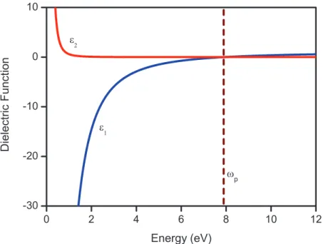
Therefore, in the low frequency regime metals are mostly absorptive. The Fig. 2.1 and Fig. 2.2 shows the ² and ˜n of silver as a function of energy. The ² and
˜
n of silver are plotted as a function of energy according to Drude model with τ = 1.45 × 10¹³s−1(≡ 0.06eV ) and ω
p = 1.2 × 10¹⁶rads−1 In Fig 2.1 blue curve
represents ²1 and red curve represents ²2. The wine line stands for the plasma
frequency. It is clearly seen that ²1 changes sign at ωp. It is negative below this
frequency and positive above it. Above this frequency metal becomes transparent to the applied electric field.
CHAPTER 2. FUNDAMENTALS OF SURFACE PLASMON POLARITONS6
Figure 2.1: Real(²1) and imaginary(²2) parts of dielectric functions calculated
using Drude model.
Figure 2.2: Refractive index (blue line) n and extinction coefficients (red line) κ calculated from Drude model.
Figure 2.3: Real(²1) and imaginary(²2) parts of dielectric functions calculated
from Drude model (lines) and experimentally measured values (dots).
2.1.2
Optical Constants of Real Metals
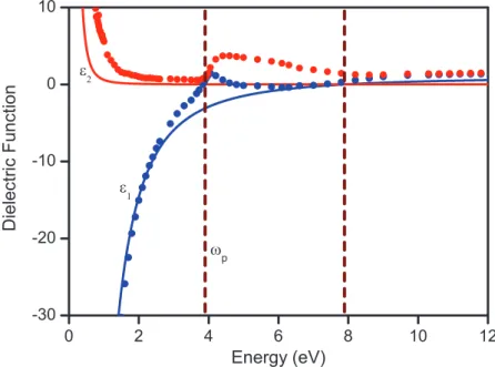
Drude’s free electron model fails in the visible and ultra violet regime for noble metals which are materials of choice of many plasmonic applications. Therefore, it is important to describe the dielectric function of the metals accurately. The color of the noble metals are different although Drude model estimates nearly the same plasma frequency corresponding to same color for these metals. The quantum theory explains the difference by the interband transitions occurring between d to sp bands. The electron configuration of gold and silver are [Xe]4f145d106s1
and [Kr]4d105s1, respectively. For silver 4d and 5s orbitals are just below the
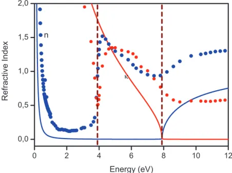
Fermi level. The energy difference between orbitals are in the order of 1.1 eV ∼ 1 µm shifting the plasma frequency of silver to 3.9 eV . The polarized interband excited electrons modify the dielectric behavior resulting in a drop in the reflection spectrum and giving rise the characteristic color of the metal[8]. Fig. 2.3 and Fig. 2.4 shows the difference and similarities between measured values and Drude model calculations of the dielectric function and refractive index. It is clearly seen that the resonance freqeuncy shifts from 7.9 eV to 3.9 eV . Practically, Drude model is easily used in to the time-domain based numerical solver such as FDTD
CHAPTER 2. FUNDAMENTALS OF SURFACE PLASMON POLARITONS8
Figure 2.4: Refractive index n and absorbtion coefficients κ calculated from Drude model (Lines) and experimentally measured values(Dots)
since the model allows to write induced current directly[7].
2.2
Characteristics of SPP
In this section, first we will review the derivation of dispersion relation for SPPs and show the field distribution of SPPs. Next, we will review characteristic scales for SPPs as a function of index, wavelength, propagation distance and penetration depths of SPPs.
2.2.1
Dispersion of Surface Plasmon Polaritons
From the wave equation as a start, one can derive the dispersion relation of SPPs from Maxwell equations. Wave equation will be solved in regions with constant dielectric permittivity together with the boundary conditions. To describe the confined wave propagating at the interface first, we will define the geometry and the time dependenceof the field. In Fig. 2.5 the geometry is shown, dielectric
x y z x z Metal Dielectric a) b)
Figure 2.5: a)The propagation geometry. b)xz plane of propagation geometry permittivity is constant in the xy plane and changing abruptly at z = 0. It equals to ²1 above z = 0 to ²2 below z = 0. x is the propagation direction.
The propagating wave can be written as E(r, t) = E(z)eiβxe−iωt with a harmonic
time depence. β is the propagation constant along the x direction. Inserting the expression into the electromagnetic wave equation, we obtain:
∂2E(z)
∂z2 + (k0² − β
2)E = 0. (2.12)
where k0 = ωc. A similar equation can be written for H component. Propagation
in the x direction and homogeneity in the y direction, (∂
∂y = 0) simplifies and
decouples equations into two polarizations: TM and TE modes. Here, we show only the solutions for the TM mode,
Ex = −i 1 ω²0² ∂Hy ∂z , (2.13) Ex = β ω²0² Hy, (2.14) ∂2H y ∂z2 + (k0² − β 2)H y = 0. (2.15)
Now, we write the field components which are propagating along the x direction and are confined to the interface. The field components for z > 0 can be written as: Hy(z) = A2eiβxe−k2z, (2.16) Ex(z) = iA2 1 ω²0²2 k2eiβxe−k2z, (2.17) Ez(z) = −A2 β ω²0²2 eiβxe−k2z. (2.18)
CHAPTER 2. FUNDAMENTALS OF SURFACE PLASMON POLARITONS10
For z > 0 the solutions are:
Hy(z) = A1eiβxe−k2z, (2.19) Ex(z) = iA1 1 ω²0²2 k2eiβxe−k2z, (2.20) Ez(z) = −A1 β ω²0²2 eiβxe−k2z. (2.21)
where k1 and k2 are both positive and restricts the confined behavior along the
z direction. Boundary conditions restricts the continuity of Hy and Ex at z = 0
plane and result with:
A1 = A2 (2.22) k2 k1 = −²2 ²1 (2.23) It should be noted that k1 and k2 are positive, so the ² of the media should be of
the opposite sign to satisfy Eq.2.23. These surface waves can only occur at the interface of materials with dielectric constants of opposite sign, such as metal-dielectric interface. On the other hand Hy should also satisfy Eq.2.15, namely:
k2
1 = β2− k02²1, (2.24)
k2
2 = β2− k02²2. (2.25)
We can combine both Eq. 2.23-2.25 and find the dispersion relation of surface plasmon polaritons as:
β = k0
s
²1²2
²1+ ²2
. (2.26)
Dielectric permittivity ² for dielectrics is usually constant over a wide range of frequencies compared to metals. On the other hand, metals are very dispersive materials such that ² of silver changes dramatically from −0.6209 + i0.01570 to
−159.6131 + i15.5259 for wavelengths in the range of 200 to 2000nm. Also it
should be noted that β is always larger than k0 which indicates the nonradiative
behavior of surface plasmon polaritons. Also, due to the difference between k0and
β, photons cannot directly excite SPPs. Fig. 2.6 shows the dispersion relation
according to this expression modelling the dielectric constant of metal according to Drude model. The bounded nature of SPPs can be seen from the dispersion curve relies below the light line. For frequencies above ωp the dispersion curve
Lig ht Lin e (Ai r) Lig ht L ine (Pri sm) SPP ωsp
Figure 2.6: Real part of the SPP Dispersion relation at silver-air interface (Blue Line). Imaginary part of the SPP Dispersion relation at silver-air interface.Light line in air (Brown Line) and prism (Gray Line)
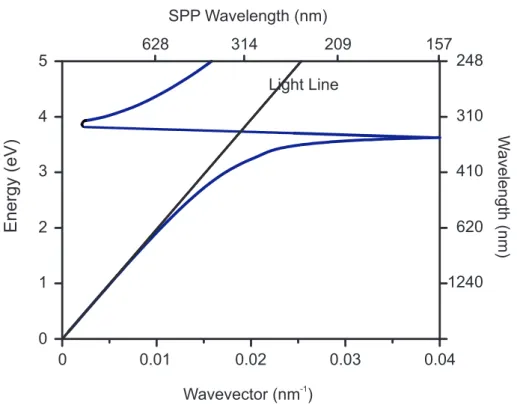
CHAPTER 2. FUNDAMENTALS OF SURFACE PLASMON POLARITONS12 En e rg y (e V) Wavevector (nm )-1 W a ve le n g th (n m ) 1240 620 410 310 SPP Wavelength (nm) 628 314 209 157 0.01 0.02 0.03 0.04 0 0 1 2 3 4 5 248 Light Line
Figure 2.7: The SPP Dispersion relation at silver-air interface (Blue Line) is above the light line and these modes are called radiative modes. For small wavevectors, propagation constant β and k0 are very close to each other. For
larger wavectors, inserting ² of the metal into dispersion relation for SPPs gives us the characteristic surface plasmon frequency, wsp. There is a natural gap between
ωp and ωsp where propagation is not allowed because the propagation constant
β takes imaginary values. However, Drude model fails to estimate values of ωp
and ωsp and the behavior between these frequencies.The Fig.2.7 shows the actual
relation of SPP with corrected ² characteristic of metal. The plasma frequency shifts to 3.9 eV and surface plasmon frequency shifts to 3.7 eV due to additional d orbital transitions. The region between ωp and ωsp can be experimentally excited
and these modes are called as quasi-bounded modes.
2.2.2
Field Distribution of SPP
Fig. 2.8 shows the field distribution of SPPs at the metal-dielectric surface. The electric fields originate from positively charged sites of the metal and end with
Figure 2.8: Electric and Magnetic field distribution of Surface Plasmon Polariton propagating at metal-air interface (TM case).
CHAPTER 2. FUNDAMENTALS OF SURFACE PLASMON POLARITONS14
the negatively charged sites. Electric field has both parallel and perpendicular components at the interface while H has only paralel components. The direction of perpendicular electric field components in two media are opposite, while the direction of parallel components are the same. The boundary conditions require the continuity of D⊥ = ²E⊥ and Ek. Having a metal-dielectric interface with
²s being negative and positive guarantees the continuity of D⊥ and E⊥. The
impossibility of TE polarized SPP is based on absence of magnetic monopoles, resulting in a divergence free H fields. This means that originating and end points of H fields are the same. The H field is divergence free, however boundary condition restricts that Hk should be continous but H have opposite directions
at metal dielectric interface due to its divergence free nature. Therefore the TE polarized SPPs cannot fullfill the boundary conditions and can not be excited at metal-dielectric interfaces. A detailed explanation can be found in [9].
2.2.3
The compex refractive Index of SPP
Defining an effective index for SPPs produces a deeper understanding for the bound behavior of SPP. The dispersion relation of SPP can be simplified as
kSP P = ωc(1 + 2|²1m1|+ i2(²²m2m1)2) if ²m2<< |²m1| and |²m1| >> 1. Then the effective
index for SPP can be expressed as:
nSP P = 1 + 1
2|²m1|
+ i ²m2 2(²m1)2
(2.27) Note that real part of the nspp is always larger than 1, which indicates the bound
baheviour of a SPP. The corresponding momentum for SPP is p = ¯hkSP P is larger
than momentum of free photon p = ¯hk0. The imaginary part determines the loss
which will be discussed later.
2.2.4
SPP Wavelength
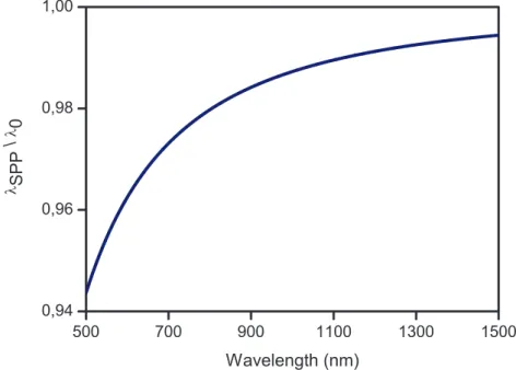
The period of the surface charge density oscillation and field distribution describes the wavelength of SPP. The real and imaginary parts of the dispersion relation
Figure 2.9: Normalized surface plasmon polariton wavelength at silver-air inter-face. The Drude model is used to characterise silver
describes the wavelength and propagation length of SPP respectively. The real part of the SPP wavevector is
kSP P0 = k0
s
²d²m1
²d+ ²m1
. (2.28)
The SPP wavelength can be written from λSP P = kSP P2π and found as:
λSP P = λ0
s
²d+ ²m1
²d²m1
. (2.29)
From Fig.2.9 it is seen λSP P is larger than λ0. This reduction in the wavelength
make SPPs suitable for diffraction limited applications. The wavelength of SPP shrinks to 70 nm at ωsp where the wavelength of a free photon with same energy
is 310 nm. In the visible regime this reduction effect is not very important since the ratio of SPP and free photon wavelength is about 0.9 [10].
2.2.5
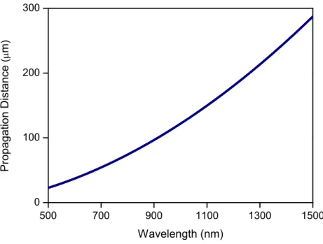
Propagation Distance of SPP
The main factor reducing propagation distance is the metallic losses. Due to imaginary part of the wavevector in the propagation direction has imaginary
CHAPTER 2. FUNDAMENTALS OF SURFACE PLASMON POLARITONS16 500 700 900 1100 1300 1500 0 100 200 300 P r o p a g a t i o n D i s t a n c e ( m ) W avelength (nm)
Figure 2.10: The propagation length of the surface plasmon polariton. The Drude model is used to characterise silver
part, the SPP intensity reduces from loss as it propagates. The propagation distance δSP P can be defined as the length where the power decreases to 1/e of
value. The propagation distance is defined by δSP P = r
1 2kSP P00
and can be found as[10]: δSP P = λ0 (²m1) 2π²m2 (²m1+ ²d ²m1²d )32. (2.30)
The ways to increase propagation distance is to use different geometries for guding of wavelength or using gain media [11].
2.2.6
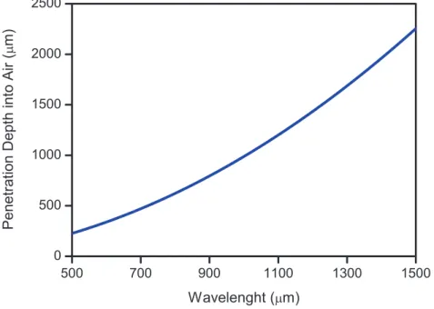
Penetration Depths of SPP
The SPP field is confined to the interface. It decays into both dielectric and metallic medium. The penetration depths are the length where perpendicular (to interface) component of electric field Ex falls to 1/e of its value. It was
characterized by kx which can be found from the expression for total wavevector:
Figure 2.11: The penetration depth of the surface plasmon polariton into air. The Drude model is used to characterise silver
where ²i stands for dielectric constants of metal and dielectric mediums. Then
inserting Eq. 2.26 into Eq. 2.31 we can define penetration depths in metal and dielectric as δm and δd: δm = 1 k0 | ²m1²2+²d m | 1 2 , (2.32) δd = 1 k0 | ²m1²+²2 d d | 1 2 . (2.33)
The details can be found in [10].
The penetration depth in the dielectric and the propagation length decrease as the wavelength decreases. In other words as the filed localizes along the metal-dielectric interface, the metallic increases and propagation distance decreases[10].
2.3
SPP Coupling
As the dispersion relation reveals, SPP dispersion curve lies below the light line. So there is a necessity to use special phase matching techniques to excite SPPs.
CHAPTER 2. FUNDAMENTALS OF SURFACE PLASMON POLARITONS18
There are numerous techniques to excite SPP such as with charged particles, prism couplers grating couplers, near field coupling . The detailed expalanations can be found [7]. Here we will focus on the prism coupling and the grating coupling method.
2.3.1
Prism Coupler
The method is based on attenuated total reflection (ATR) to excite SPP. The configuration is shown in Fig. 4.1a. The prism is a high index prism which can enhance the momentum of the incident photon. The momentum of SPP is larger than k0 and to excite an SPP, the parallel k vector component of the incoming
photon should be equal to kspp. k vector of incoming photon is increased to
nprismk. The coupling condition is given by:
kSP P = k0nprismsin(θ) (2.34)
where nprism and θ) are refractive index of the prism and angle of incidence
re-spectively. The resonance condition can be found through scanning the angle of incidence. The reflected beam intensity goes to a minimum when an SPP is excited. Incident light penetrates through the metal/air interface and partially reflects. SPP also reradiates through the prism and the radiated field interfere with each other. The minimum in the reflected spectrum occurs due to destruc-tive interference between the reradiated SPPs and reflected light at prism-metal interface. The metal thickness is important to reach a perfect dip in the reflection spectrum.
2.3.2
Grating Coupler
Gratings can also supply the momentum needed to excite SPPs. Periodic patterns on the surface can increase the momentum of the incoming light. Using this property of gratings SPPs on both sides, above and below a grating can be excited. The coupling condition is given by this condition
k0
α
np
k0
kSPP
kSPP
a)
b)
kSPP
CHAPTER 2. FUNDAMENTALS OF SURFACE PLASMON POLARITONS20
where θ,G = 2π
λ are angle of incidence of incoming photon and reciprocal vector
of the grating respectively with m = (0, 1, 2...). Similarly in the case partially reflected beam and reradiated SPPs interfere destructively and a minima in the reflection spectrum is observed. By changing the incidence angle and wavelength of the photon available, SPP excitations can be measured. The configuration is shown in Fig4.1b.
2.4
Propagation of SPP on Periodic Surfaces
In this section we review the SPP propagation on the periodic surface. We will use the analogy between energy band gaps in condensed matter physics, photonic band gaps in photonic band gap materials and crystals and plasmonic band gaps. In condensed matter physics, energy bands occur due to interaction of the con-duction electron with the ion cores of the crystal. At Bragg resonance no wavelike solutions exist. At these wavevectors, left propagating waves are back reflected. The solution of these waves are standing waves and two different standing wave configuration can be constructed. These two standing waves have different spa-tial distributions and experience different parts of the crystal potenspa-tials. One is located on the cores of ions, the other one is between the ion cores. The potential experienced by these two standing waves are different, so the average expected energy values are different for these standing waves. Thus, a band gap is opened between these energies[12]. For the photonic case, media with different refractive indices serve as high and low potential regions for photons. The periodic con-figuration of this medium is known as photonic crystal. When the light beam is incident onto these structures, there will be scattering at each interface in the structure. If the wavelength of the light is twice the optical periodicity, Bragg condition will be satisfied and the light will be back reflected. These waves will destructively interfere with each other and form a standing wave similar to the electronic case. The configuration of these standing waves will be different. One configuration leads to localization on the high index material and the other on the low index material. There will be energy gap between these values similar to the electronic case, called the photonic band gap[13]. Fig. 2.13 represents
n1n2 n1n2 n1n2 n1n2n1
ω−
ω+
Figure 2.13: Electric field distributions of localised states in the photonic crystal. Lower energy configuration(ω−). Electric field localizes on the low index regions.
Higher energy configuration(ω+). Electric field localizes in the high index regions
a multilayer dielectric film with high refractive indices (n2) and low refractive
index (n2). Electric field distribution at edges of band gap are shown in Fig.
2.13. Higher energy configuration standing wave, (ω+), localizes in high index
(n2) regions and lower energy configuration standing wave, (ω−), localizes in low
index (n1) regions.
Ion cores for electrons and index difference for photons results in similar ef-fects. In the analogy with electronic band gaps and photonic band gaps, plas-monic band gaps are due to the corrugation of the surface. If the surface where the SPP propagates is peridocally corrugated, the corrugation act as scattering centers since the effective index along the grating changes periodically. The pe-riodic surface leads to scattering of SPPs. When the Bragg condition is met, a band gap opens up. The localized SPPs have different configurations[14]. The Fig. 2.14 represents two electric field distributions of SPPs at the edges of plas-monic band gaps. Siminlar to photonic and electronic case, localization sides of SPP on grating are different for two cases. As seen in Fig. 2.14a the positive and negative charges are localized on the peaks. In the other case, the charges
CHAPTER 2. FUNDAMENTALS OF SURFACE PLASMON POLARITONS22
++
--
++
--
++
--
--E
++
--
++
--
++
--E
a)
b)
ω
−
ω
+
Figure 2.14: Electric field distributions of localised states on the grating. a)Lower energy configuration. Charges localizes on the peaks. b) Higher energy configu-ration. Charges localizes on the througs.
are localized on the thoughs. The factor that determines the difference in energy of the modes is the distortion in the field lines. Fig. 2.14b represents a more distorted field distribution resulting in a higher energetic mode. Besides the en-ergy difference between these two modes, their confinement behaviors are also different which will be discussed with details in Chapter 5.
2.5
Dispersion of SPP on Periodic Surfaces
There is a momentum mismatch between free space propagating photon and the excited bound plasmon, having the same energy. The dispersion curve for light line lies above the dispersions of bound SPP as seen in Fig. 2.15a. As we discussed in the previous section, excitation of SPP on flat metal surface is forbidden. However, when we consider the dispersion of free photon in prism, its dispersion line lies below the light line in air as seen in Fig. 2.15b. There is a point where dispersion of SPP and dispersion of free photon in prism intersect. SPP can be excited at that point. We can excite SPP resonances by the prism coupling technique discussed above. The Fig. 2.15c shows the dispersion of SPP on a periodic surface. The band gap formation takes place for periodic surfaces at the edges of Brillion zone. However, the dispersion of SPP still lies above the light line , the momentum mismatch condition prohibits the excitation of SPPs. Applying the prism coupler technique, the SPP dispersion in Fig. 2.15c can be observed. The Fig. 2.15d indicates the resulting dispersion curves. The periodic surface is placed on the prism and SPP curve can be observed by scanning the angle of incidence and wavelength.
2.6
Localization of SPP
In this section, we will review the physical principles behind the formation of plasmonic cavities. We will make anology between photonic cavities in photonic crystals and plasmonic cavities. Then, we will show the attempts to demostrate
CHAPTER 2. FUNDAMENTALS OF SURFACE PLASMON POLARITONS24 k k k k a) b) c) d) kSPP kSPP kSPP kSPP K=2π/Λgr K/2 K/2 K/2 K/2 ω ω ω ω Λgr
Figure 2.15: a) Dispersion curves of light line in air, SPP on flat metal surface. b) Dispersion curves of light line in air and prism, SPP on flat metal surface c) Dispersion curves of light line in air, SPP on a metallic uniform grating surfaceflat d) Dispersion curves of light line in air and prism, SPP on a metallic uniform grating
cavity formation in plasmonic structures in the literature.
It was announced that breaking the symetry in photonic band gap results in localized modes in the photonic band gap[13]. Then photonic cavity forma-tion is demonstrated in the microwave and optical regimes in one, two and three dimensions[]. If we have a periodic multilayer dielectric as dicussed in the previ-ous section before we observe a photonic band gap. However, we can break the symetry along the photonic crystal by adding an additional dielectric layer in this multilayer geometry. In this case a photonic cavity mode appears in the photonic band gap. The physical reason behind this localization is the constructive inter-ference of the photons for that specific wavelength. The conditions and length of layers for the formation of this cavity is discussed in detail at [13].
Formation of plasmonic cavity can be also achieved by breaking the symetry in plasmonic band gap structures. The use of Bragg gratings for localization of prop-agating surface plasmons was suggested in 2007[15]. The cavity was composed of a thin film surface. Both right and left side of the thin film was surrounded by one dimensional Bragg gratings. The symetry breaking condition is satisfied using a thin film area in the Bragg grating region. The physical reason behind the localization of SPP is the constructive interference of SPP in the cavity region similar to photonic case. The phase change experienced by SPP after a round-trip in cavity should be equal to reflected phase shifts on the Bragg gratings at the cavity. Then the cavity mode is achieved [15]. Similar approach was used to suggest plasmonic cavities for applications in quantum electro dynamics [16].
The physical reason behind the cavity formation for SPPs is controlling the phase changes experienced by SPPs. Removing grating ridges or using thin films surrounded by Bragg gratings support this condition. Using Moire patterns also enables localization of SPPs. Moire patterns having π shifts at its nodes acts as plamonic cavities[17]. Another way to control phase changes and demonstrate formation of plasmonic cavities is selectively coating the surface with a high index dielectric[18]. Here the effective indices seen by SPPs on dielectric coated and uncoated parts are different. This difference brings a phase shift and brings reso-nance. Whenever a resonance condition is met, SPPs at that specific wavelength
CHAPTER 2. FUNDAMENTALS OF SURFACE PLASMON POLARITONS26
constructively interfere and a cavity mode is achieved. Experimental demonstra-tion of plasmonic cavities on Moire surfaces and biharmonic gratings have been achieved recently by our research group. The details of the experimental and numerical results for Moire patterns and biharmonic gratings will be discussed in Chapter 5.
Fabrication and Measurment
3.1
Fabrication of Plasmonic Structures
This section provides the methods for fabrication of plasmonic gratings and their experimental characterization. Interference lithography is a widely used optical technology to produce periodic surfaces on large areas. It is a cornerstone tech-nology for most Bragg grating devices. The physics behind this techtech-nology is the interference of two spatially coherent beams resulting in a standing wave pat-tern. The standing wave pattern consists of periodic fringes representing intensity maxima and minima. The two coherent plane waves overlapping in space and re-sultant standing waves are recorded on a photosensitive polymer. The periodicity is given by:
Λ = λ
2sin(θ) (3.1)
where Λ, λ and θ are periodicity of the grating, wavelength of the incoming light and angle between beams. In principal, a perfectly periodic pattern which is spatially coherent can be attained using this method. By spatially coherent we mean that the positions of all peaks can be known whenever position of one peak is known. The spatial coherence or in other words how the pattern is perfectly periodic is related to spatial and temporal coherence of the interfering beams. To support temporal coherence monochromatic light is needed. A laser
CHAPTER 3. FABRICATION AND MEASURMENT 28 He-Cd Laser Lens 10 µm Pinhole Llyod Mirror
Figure 3.1: The interference setup used for fabrication of gratigs. The laser beam follows the lens-pinhole path. Expanded beam from pinhole reaches to Llyod mirror
can be used. The spatial coherence guarantees uniform wavefronts of plane waves. Using pinholes and spatial filters enables attaining uniform wavefronts. The Fig 3.1 illustrates the interference lithography we used for fabrication of gratings. A HeCd laser at 325 nm is used as the illumination source. First, the fused silica lens focuses the beam at its focal point, which is on order of mm’s. The focused beam then goes through a 10 µm pinhole at the focal point of the lens. By using this pinhole we are able to eliminate nonuniformities and improve spatial coherence of the beam. The beam diverges after it passes through the pinhole and reaches to the Lloyd mirror as seen in Fig.3.1. The periodic pattern is recorded on the photosensitive polymer. The preparation of the sample can be summarized as: First a photosensitive polymer (S-1800) is spun on to a 100 um thick lamella. Then it is baked at 1100C for one minute. After it is exposed at the interference
setup, we put it in the developer to attain actual pattern physically. One of the problems with the interference lithography is that the interfering beams are not exact plane waves. Since the pinhole acts as a point source, the beams are actually spherical waves. This spherical behavior prevent obtaining perfectly periodic structures. However this effect is a very small. The main advantage of interference lithography is in making large area gratings, easily. The resolution is ideally limited by λ/2 that is 162.5 nm = 325/2 nm usually not available by optical lithography.
We use soft lithography to transfer the grating structures onto other sub-strates and materials. The transfer method enables us to examine the effect of
a)
b)
c)
d)
e)
f)
Figure 3.2: The steps of transferring a gratingin structure on photoresist on OG146
CHAPTER 3. FABRICATION AND MEASURMENT 30
different thicknesses of metal films, dielectric films on the samples which have exactly the same geometry. Using this method, we transfer grating structures onto substrates which are resistive to chemicals such as acetone and these sub-strates are suitable for photolithography processes. We can photolithographly define patterns on these substrates, in our case leading to a cavity geometry, otherwise making patterns on the grating structure in the photoresist may de-stroy grating geometry. Soft lithography is a family of techniques for fabricating or replicating patterns. Elastomeric stamps, molds and comformable masks are used during soft lithography. The word soft comes from the usage of elastomeric materials. Elastomers which are conformable and easily peel of surfaces are the polymers which have elasticity property. The steps of the transferring process is shown in Fig. 3.2. The master grating structure on the sample is recorded on a photosensitive polymer (S-1800) which is spun on a 100 um thick lamella with in-terference lithography, described above. Typically, the periodicity is 300 nm and the size of the wafer is 2.4x3.2 mm. Liquid PDMS (Sylgard 184, Dow Corning) is poured on top of the master grating which was cured for 2 hours at 750C. After
the curing procedure, the elastomeric mold is removed from the grating surface. The low Young modulus of the PDMS makes the feature sizes. Due to thermal expansion during the curing process the periodicity of the grating is reduced by 1 − 2%. However, the uniformity is still preserved. The PDMS grating surface is then ready to be used as a stamp and transfer the pattern onto a photocurable prepolymer. The UV curable low viscosity prepolymer is spun on the lamella at 4300 rpm. The thickness of the polymer is around approximately 1 µm. The PDMS stamp is placed onto the polymer spun lamella without any pressure. The conformal contact on the surface leads to the attachment of PDMS to polymer coated surface. Due to capillary action, OG 146 fills the groves of the PDMS in seconds. The sample composing of PDMS and lamella is put under UV light for 2 minutes. The OG146 which was initially liquid is cured under UV light and solidifies. After the curing process, the PDMS stamps was mechanically peeled off. The solid polymer which has the pattern on the PDMS is left on the lamella. Thus, the transfer of the grating is successfully completed. A 50 nm-thick Ag film is evaporated on the samples to support metallic surfaces for excitation of SPPs.
Prism
Index Matching
Fluid
n
n
Source
Detector
Figure 3.3: The schematic of optical characterization of plasmonic structures. SPP is excited by prism coupling technique.
3.2
Characterization of Plasmonic Structures
The characterization of samples was done by carrying out reflection measure-ments. Fig. 3.3 represents a simplified schema of our measurement setup.We used Kretchman geometry to overcome momentum mismatch and excite SPPs. A BK7 right angled prism is used in the experiment. An index matching fluid between the samples and the prism is used to minimize undesired reflections. The reflection measurements are done with a recogfigured variable angle spec-troscopic ellipsometer W-VASE32. The ellipsometer is connected to a HS-190 monochromator to provide quasi monochromatic light from a white light source. The monochromator provides desired wavelengths for the system. There is an arc lamp filled with high pressure (above the athmospheric pressure) Xenon gas. When the lamp power is turned on, a high voltage pulse is sent through the lamp causing an arc to start the lamp. Lower DC voltage maintains to support arc. The lamp is mounted in the monochromator lamp housing. The focal length of the monochramotor is 160 mm and effective aperture ratio is f/4.5. The spectral range of the monochromator is 250-1700 nm. We have typically used the 500-750 nm regime. The light is coupled from the exit of monochromator to a fiber optic cable, where the beam is collimated and polarized. The fiber optic cable enters the input unit where additional polarization states are added. Here we do not list details of the ellipsometer such as autoretarders, analyzer etc. which are also used for thin film thickness and refractive index measuresments. Since
CHAPTER 3. FABRICATION AND MEASURMENT 32
Figure 3.4: The reflection spectra of flat Ag film taken in the Kretchmann geome-try for TE and TM modes. The minima in the TM case stand for SPP excitation at metal-air interface
we perform only reflection measurements, important parts of the ellipsometer for our experiments are limited to monochromators and detectors. The samples are aligned in the x, y, z directions using a sample stage. The detector is placed at the end of the detector unit, converts light energy into voltage. The goniometer base together with the sample stage and input unit is used to precisely control the angles of incidence with a precision of 0.0010 degrees. An experimental data
is shown from our measurements in Fig. 3.4. We look the SPP coupling on a flat metal surface in the Krecthman geometry. We have carried measurement for TE and TM modes seperately. The metallic film thickness is 50 nm. The results are shown in Fig. 3.4. We observe an absorbtion peak around 600 nm at an angle of incidence 420 indicating SPP excitation. For TE case there is no resonance
1D Grating Based Plasmonic
Cavities
In this chapter, a comparative study on grating based plasmonic band gap cavities is presented. Numerically, we calculate the quality factors of the cavities based on three types of grating surfaces; uniform, biharmonic and Moir`e surfaces. We show that for biharmonic band gap cavities, the radiation loss can be suppressed by removing the additional grating component in the cavity region. Furthermore, due to gradual change of the surface profile around the cavity region, Moir`e type surfaces support cavity modes with higher quality factors. Experimentally, we demonstrate the existence of plasmonic cavities based on uniform gratings. Effective index perturbation and cavity geometries are obtained by additional dielectric loading. A quality factor of 85 is obtained from the measured band structure of the cavity
4.1
Introduction
It is well known that metallic periodic structures exhibit modified transmission and reflection spectra owing to the interaction of the propagating SPPs with the periodicity. Many features of these SPPs that are excited on periodic metallic
CHAPTER 4. 1D GRATING BASED PLASMONIC CAVITIES 34
surfaces are extensively studied. Surface enhanced Raman scattering and pho-toluminescence signals have already been observed on such structures [19]. In contrast to localized SPPs on nanoparticles, propagating SPPs on periodic sur-faces are also being studied in nanolithography and nanophotonic applications [20]. Recently, plasmonic cavities that use Bragg reflectors and selective dielec-tric loading have been under investigation[16][18][15]. In addition to uniform gratings, biharmonic gratings and Moir`e surfaces can be used to construct cavity structures. Such cavities can localize plasmons and can lead to small group ve-locities around the band edges. While these structures all localize the plasmons, they exhibit different characteristics due to the difference in their design and the mechanism of confinement.
On the other hand, metallic loss at visible wavelengths is a serious problem that hinders the use of plasmons for applications that require long propagation lengths and plasmonic lifetimes. Due to this same reason, current cavities with relatively low quality factors need to be improved to meet expectations. Large quality factors for SPPs, localized in cavities, are crucial for many applications. A cavity designed for localization of SPPs with high quality factors can be used to selectively enhance and suppress spontaneous emission rates of emitters and may provide an ideal platform for cavity quantum electrodynamics (QED). SPP cavities that are expected to work in the strong coupling regime with large Pur-cell factor enhancements have been suggested. Quality factors as high as 1000 have been proposed [16]. Bragg mirrors used in so many photonic structures have been suggested for simple confinement in one dimension and have been shown to exhibit enhanced Purcell factors for applications in cavity QED. Such mirrors have also been employed for SPP localization and characterized with scanning near field optical microscopy to map the electric field distribution in and out of the cavity. Results confirm the cavity formation and localization of the SPP modes. Alternatively, using double exposure interference lithography, biharmonic gratings were employed to localize SPPs. The quality factor of the demonstrated plasmonic cavity was 37 due to metallic and scattering losses in the cavity [18]. Very recently, Moir`e surfaces have been demonstrated to support SPP localiza-tion at the nodes of a metallic Moir`e surface. Smooth varialocaliza-tion of the surface
a)
b)
c)
Figure 4.1: Surface profile of a) uniform, b) biharmonic and c) Moir`e gratings. Note the selectively coated dielectric (red line) on the biharmonic and uniform gratings and the cavity region. Localization takes places around the node of the Moir`e surface.
relief amplitude in these structures reduces radiative losses leading to relatively high quality factors (Q=103) [17]. The increased quality factor is promising and suggests further study. Experimentally, we demonstrate plasmonic cavity forma-tion on uniform metallic gratings, which consists of a single periodic surface as shown in Fig. 4.1a. Because surface plasmons are sensitive to the effective index of the medium, localization on uniform gratings have been achieved by selectively coating the metallic surface with silicon. To couple light to the surface plasmons, Kretchman configuration is used to overcome the momentum mismatch between surface plasmons and incoming light. The band gap is provided by the uniform metallic grating while the prism allows the SPP excitation [14]. The character-istics of the Q factor of plasmonic cavities on uniform, biharmonic gratings and Moir`e surfaces are studied numerically. The biharmonic grating, as shown in
CHAPTER 4. 1D GRATING BASED PLASMONIC CAVITIES 36
SPP excitation and band gap formation are achieved by using the grating com-ponents. The plasmonic cavity mode is obtained through selective loading of the metallic surface. Numerical results indicate that as the amplitude of the larger component is increased the quality factor decreases. The Moir`e surface which
is a superposition of two periodic surfaces with slightly different periodicities as shown in 4.1c also support plasmonic cavities. The phase shift at the nodes of the surface leads to localization of the SPPs. The slowly varying grating amplitude around the cavities results in higher quality factors. Different Moir`e surfaces are studied to compare their respective quality factors.
4.2
Fabrication and Experiment
Fabrication of a uniform grating was achieved with an interference lithography setup as we discussed in Chapter 3. We, first spin a photosensitive polymer (S1800) on 170 µm thick microscope lamella and bake the photosensitive polymer at 1100C for 1 minute. A 325 nm He-Cd laser was used to record periodic
struc-tures on the photosensitive polymer using Lloyd’s mirror configuration. Once the structures were developed, they were transferred onto a photocurable polymer (OG146) by the nanoimprint technique. Biharmonic gratings and Moir`e surfaces require double exposure of the periods. A 50 nm thick silver film was evaporated on the OG146 polymer to support the surface plasmons. The lamellae was then mounted on the base of the prism with the metallic side up and index matching fluid was used between the prism and the lamallae. The BK7 prism allows in-coming photons to couple to the plasmons. The coupling condition is satisfied at a specific wavelength and angle of incidence. This condition is given by
kSP P = nEF Fk0 = npk0sin(θ) (4.1)
where kspp and nef f are the wavenumber and the effective index of the SPPs. k0,
θ and np are the free space wavenumber of incident photon, angle of incidence
and refractive index of the prism, respectively. The dispersion curves of SPPs are constructed by measuring the coupling wavelength and angle. We used a spectroscopic ellipsometer (VWASE32) for precise reflectivity measurements. The
Figure 4.2: Reflectivity spectra of a) flat metallic surface, b) uniform metallic grating, c) uniform metallic grating coated with 10 nm of silicon.
reflection measurements at different angles of incidences result in two dimensional reflectivity maps. In order to construct the band structure with high resolution, we scanned the 500-750 nm wavelength range at various angles of incidence with a resolution of 0.2 apart.
4.3
Uniform Plasmonic Band Gap Cavities
In Fig.4.2, wavelength dependent reflection spectra of three different structures are shown with the corresponding experimental configurations. Fig. 4.2a shows the reflection spectra of the TM polarized light from a flat metal surface. As ex-pected, we observed the plasmon resonance at the wavelength of 580 nm. How-ever, periodic structure on the surface modifies the dispersion relation. This modification is manifested in the reflection spectrum of a uniform grating and is shown in Fig. 4.2b. Propagating SPPs interact with the grooves of the grating and are backscattered. This leads to the formation of standing SPP waves on the uniform grating. Symmetry suggests the presence of two standing waves, labeled
λ− and λ+, with two different energies. One localizes on the peaks and the other
on the troughs of the periodic structure [11]. A band gap is opened up due to the energy difference between λ− and λ− modes. The gap is located approximately
at 600 nm with the band edges observed at 560 and 635 nm. The width of the band is 23 nm. When the uniform metallic grating is coated with a thin layer of silicon, the effective index experienced by the SPP mode increases, and opens up the band gap. The reflectivity spectra of the uniform metallic grating coated with
CHAPTER 4. 1D GRATING BASED PLASMONIC CAVITIES 38
α
Power Monitor Source Air
Dielectric
α
Power Monitor Source Air Dielectric a) b) c) d) R e fl e ct ivi ty (a .u .) 550 575 600 625 650 Wavelength (nm) R e fl e ct ivi ty (a .u .) 550 575 600 625 650 Wavelength (nm) λ− λ+
Figure 4.3: Schematic representation of simulated structure for a) flat metallic surface, b) uniform metallic grating. FDTD simulation results of reflectivity measurements for c) flat metallic surface, d) uniform metallic grating
10 nm of silicon is shown in Fig. 24.2c. Red shift of the spectrum and opening up of the band gap are clearly observed. The red shift is due to the effective index change, induced by silicon. The widening of the band gap comes from different confinement properties of λ− and λ+ modes on the grating surfaces. The low
frequency mode is confined closer to the surface of the samples while the higher frequency component has a longer evanescent tail.
The different confinement behavior of λ− and λ+ can be understood better
with the numerical investigations. We have employed the Lumerical software pro-gram to examine the plasmonic characteristics of the structures. The propro-gram uses finite difference time domain (FDTD) technique to obtain optical charac-teristics of the structure. The details of the computational method is given in Appendix A. We have used nonuniform mesh around metal-dielectric interfaces,
λ/10 mesh size is used for uniformly meshed parts of the simulation area and
2.0 nm mesh size is used for the nonuniform meshing area. We first studied the surface plasmon excitation on a flat metal surface. The simulation geometry is
In te n si ty (a .u .) 0 0.4 0.8 1.2 In te n si ty (a .u .) 0 0.4 0.8 1.2
λ−
λ+
a)
b)
c)
d)
Figure 4.4: Electric field distributions of surface plasmon polariton at band edges. a) Higher energy configuration for λ− b) Lower energy configuration for λ+
Elec-tric field intensities at the metal-air interface c) Higher energy configuration for
λ− d) Lower energy configuration for λ+
shown in Fig.4.3a and b. We launch a Gaussian wave from a dielectric medium and look at the power of the reflected light from metal-air interface. The power of reflected light is read through the monitor in the simulation domain. The re-fractive index of the dielectric medium is 1.56 and the value of dielectric function of the metal is taken from Palik [21]. The metal thickness is 50 nm. The reflec-tivity maps of the flat metal surface is studied for both TE and TM polarization states. In Fig.4.3c the reflectivity maps taken at θ = 45 are shown. The SPP excitation is seen for only TM polarized case, as expected. Next, we have inserted a uniform grating with a periodicity of 290 nm and amplitude of 20 nm similar to the experiment we described above. The geometry in the simulation is shown in Fig.4.3b. The reflectivity spectra for uniform grating is shown in Fig.4.3 The
λ− = 589 nm and λ+= 628 nm are labelled with red lines. Then we have studied
the electric field configurations of λ− and λ+. Fig.4.4a and Fig.4.4b shows the