©BEYKENT UNIVERSITY
VOLTAGE TYPE FIRST ORDER ALL-PASS
FILTER EMPLOYING FULLY DIFFERENTIAL
CURRENT FEEDBACK OPERATIONAL
AMPLIFIER AND ITS APPLICATION
A novel voltage mode first order all-pass filter configuration is proposed. The presented circuit uses a single fully differential current feedback operational amplifier (FDCFOA), resistors and a grounded capacitor. High input impedance of the proposed filter enables the circuit to be cascaded without additional buffers.It does not impose any component matching constraint in analog signal processing circuits. Moreover higher order all-pass filter could be achieved by cascading the proposed all-pass sections.In order to demostrate the performance of the proposed filter a new voltage mode oscillator is introduced as an application example. Also the theoretical results are verified with SPICE simulations using a CMOS realization of FDCFOA.
Key words: All-pass filter, fully differential current feedback operational amplifier, analog integrated circuits, quadrature oscillator.
TAM DİFERANSİYEL AKIM GERİ BESLEMELİ
İŞLEMSEL KUVVETLENDİRİCİ İLE
GERÇEKLENEN GERİLİM TİPİ 1. DERECEDE
TÜM GEÇİREN SÜZGEÇ VE UYGULAMASI
Gerilim modunda birinci dereceden tüm geçiren yeni bir süzgeç devresi önerilmiştir.Önerilen devrede bir tam diferansiyel akım geribeslemeli işlemsel kuvvetlendirici, dirençler ve topraklı bir kapasite bulunmaktadır. Önerilen
Mahmut ÜN
Dept.of Elec. & Com. Eng., Beykent University [email protected]
Fırat KAÇAR
Dept. of Elec. & Electronics Eng. İstanbul University [email protected] Received: 18 June 2007, Accepted: 26 December 2007
ABSTRACT
devrenin yüksek giriş direnci, ek tampon kullanılmadan devrenin kaskad bağlanabilmesini sağlamaktadır. Analog işaret işleme devrelerinde herhangi bir eleman denkleştirme koşuluna gerek duyulmamaktadır.Bundan başka daha yüksek dereceden tüm geçiren süzgeçler önerilen birinci dereceden süzgeçler kaskad bağlanarak elde edilebilmektedir. Önerilen süzgecin başarımını göstermek amacıyla, bir uygulama örneği olarak gerilim modunda yeni bir osilatör tanıtılmıştır. Ayrıca kuramsal sonuçlar, FDCFOA elemanının CMOS gerçeklenmesi kullanılarak SPICE benzetimleriyle doğrulanmıştır.
1. INTRODUCTION
All-pass filters are one of the most important building block of many analog signal processing applications and therefore have recieved much attention. They are generally used for introducing a frequency dependent delay while keeping the amplitude of the input signal constant over the desired frequency range. Other type of the active circuits such as oscillators and high-Q band-pass filters are also realized by using all-band-pass filters [1-6]. The active devices that have been used for the realizations of first order all-pass circuits include operational amplifiers (OP-AMP), second generation current conveyor (CCII), current feedback op-amps (CFOA), operational transconductance amplifier (OTA) and four terminal floating nullor (FTFN). Several voltage and current mode first order all-pass filters are available in the literature [2-10]. A literature survey shows that there are only a few transadmittance mode filters. Since the introduction of FDCFOA by Soliman, a few applications have appeared in the literature [10-12]. The main purpose of these paper is to propose a new application of FDCFOA as a voltage mode first and higher order all-pass filter. In this paper, FDCFOA-based voltage mode first order allpass filter configuration is proposed and also a sinusoidal oscillator is implemented to show the usefulness of the proposed configuration as an illustrating example. Furthermore SPICE simulations are performed to verify the theoretical results by using CMOS-FDCFOA realization.
2. THE PROPOSED ALL-PASS FILTER CIRCUIT
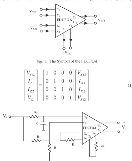
The FDCFOA is basicly a fully differential device as shown in Figure 1. The Y1 and Y2 terminals are high impedance terminals while X1 and X2 terminals
are low impedance ones. The differential input voltage VY12 applied across Y1
and Y2 terminals is conveyed to differential voltage across the X1 and X2 termianls; i.e., (VX12 =VY12). The input currents applied to the X1 and X2 are
conveyed to the Z1 and Z2 terminals are high ipmedance output nodes suitable
for current outputs. The differential voltage developed across the Z1 and Z2
terminals are buffered by a unity gain fully differential voltage buffer to the output terminals O 1 and O 2 , i.e., ( V O 1 2 = V Z 1 2 ) .
The port relations at an ideal FDCFOA, shown in Figure.1 can be given by o — • o — • o — • o — • Ô Ô Vzi2
Fig. 1: The Symbol of the FDCFOA
V , 12
1 0 0 0
V * 12 I Z 10 1 0 0
I x 1 1Z 20 0 1 0
1X 2 V12_ 0 0 0 1
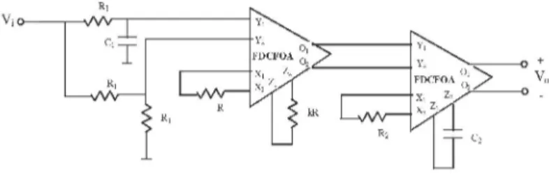
_ V Z 1 2 (1) Vi o o + Vo o _Fig. 2: The proposed voltage mode first order all-pass filter configuration
The proposed configuration is shown in Figure.2. Routine analysis yields the voltage mode transfer function as follows
1 ^
V> =
A
Ri
cV ^
2
i 5 + - (2)R1C
This transfer function allows the designer both inverting and noninverting types of first order voltage mode all-pass filters by exchanging C and R1 using
only a single FDCFOA.Thus both inverting and noninverting types of first V
V V
order voltage mode all-pass filters are realized using only a single FDCOA, resistors and a grounded capacitor.without imposing any passive element condition. Furthermore, transfer function analysis of the proposed all-pass filter can be made for the nonideal FDCFOA by following the same procedure givev for the ideal case. .
3. QUADRATURE OSCILLATOR AS AN ALL-PASS
FILTER APPLICATION
It is well-known fact that a sinusoidal oscillator can be realized using an all-pass filter and an integrator[13] as shown in Figure.3.
Vit>.
Fig. 3: FDCFOA-based sinusoidal oscillator circuit
In this circuit, the proposed allpass filter and a voltage mode integrator employing a FDCFOA with two matched resistors and capacitors are used.For providing a sinusoidal oscillation the loop gain of the circuit is set the unity at s=jw, i. e
1
(-k/2)5 -1/R
1C
1s +1/R
1C
1 s R2C2= 1
(3) s = j aFrom Eq. (3) oscillation condition and frequency can be found respectively as
( k /2) R
1C
1= R
2C
2(4)
f 1 A
1
R1C1
(5)
(5)
For simplicity, if we choose R1 =R2 = R and C1 = C2 = C , oscillation
condition is satisfied and oscillation frequency becomes
+
V1
* = IRC
< 6 )Also oscillator condition and frequency can be calculated in terms of nonideality parameters of FDCFOA for the nonideal FDCFOA. It is assumed that all FDCFOAs are ideal for all analysis given above.
4. SIMULATION RESULTS
To verify the theoritical study the first order all-pass filter was constructed and simulated with PSPICE program. For this purpose, passive components were chosen as R=1kO, R1=1kO nd C=1pF, k=2 which results in 15.92 MHz center
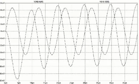
frequency. Since there is no any commerical implementation of the FDCFOA, the SPICE simulations were performed using a CMOS realization of FDCFOA [12]. Simulated magnitude and phase response of the filter is given in Figure.4. Actually, the parasitic resistance and capacitances of CMOS-FDCFOA, that is not mentioned in the limited space avaliable here, causes the deviations in the frequency and phase response of the filter from theoretical values. For either discrete or integrated implementation of the filter circuit, the designers should pay much attention to reduce the parasitics of FDCFOA. Furthermore, sinusoidal input-output waveforms of allpass filter is presented in Figure.5 for the component values given above. Oscillator employing the proposed allpass filter has also been simulated using PSPICE. In this simulation, k=2, all resistances and capacitances were taken as 1 0 k ^ and 10pF respectively which results in a 1.59 MHz oscillation frequency.The output waveforms of the oscillator are shown in Figure.6. Because of the parasitic effects of the FDCFOAs some deformations are observed in the output waveforms of the filter and oscillator.
5. CONCLUSION
A voltage mode first order all-pass filter configuration is presented.The proposed circuit uses only a single FDCFOA, resistors and capacitors. The output of the filter exhibits low output impedance so that the synthesized filter can be cascaded without additional buffers.The proposed circuit uses grounded capacitor and resistors which simplifies integrated circuit implementation. Moreover higher order all-pass filter could be achieved by cascading the proposed all-pass section. As an application of the filter, a new quadrature oscillator was realized. SPICE simulations were performed by using a fully differential CMOS-CFOA. PSPICE simulation results of the filter response are in good agreement with the predicted theory. It also provides an alternative solution to the realization of phase equalizer for analog signal processing applications.It is supposed that all FDCFOAs used in the circuits analyzed are
ideal through the paper. Anaysis of nonideal effects on the oscillator and filter circuits are leaved for the further studies.
? I OMR -¡•M SilM — • f Xlldll •y.'/t Hill--Ï.ÏUJU ? nsiiB -x-4iiiin—• / 4'irtM -¡•".MIilM —• -¿M.'j.JU--? ftflilR I I . . . 1 KHz lOKHz lOOKHz 1MHz 10MHz 100MHz Fig. 4: PSPICE simulation result of the proposed voltage-mode first-order allpass filter
(Gain:—, Phase : — )
D [is 5|ls 10|ls 15|ls 20|is 25|ls 30|ls 35|ls 40|ls 45|ls
V[10|-V(41] V[61|-V[65)
Fig. 6: Simulated output waveforms of the Quadrature oscillator (Input: • Output: • )
References
[1] Schauman, R., Valkenburg E.,: Design of analog filters. Oxford University Press, New York, 2001.
[2] Donald, T. C., David, T.C., Jason, R. G.,: A high frequency integrable band-pass filter configuration, IEEE Transactions on Circuits and Systems, 44 (1997) 856-860.
[3] Cicekoglu, O., Kuntman, H., Berk, S.,: Single CCII+ based all-pass filters, Int. J. Of Electronics, 86 (1999), 947-959.
[4] Çam, U., Cicekoglu, O., Gülsoy, M., Kuntman, H.,: New voltage and current mode first-order all-pass filters using single FTFN, Frequenz, 7-8 (2000), 177-179. [5] Higashimura M., Fukai, Y.,: Realization of all-pass and notch filters using a single
current conveyor Int. J. Of Electronics, 65 (1988), 823-828.
[6] Toker, A., Ozoguz, S., Cicekoglu, O., Acar, C.,: Current mode all-pass filters using current differencing buffered amplifier and new high-Q band-pass filter configuration, IEEE Transaction on Circuits and Systems-II, 47 (2000), 949-954. [7] Sudhanshu, S., Iqbal, A.K.,: Novel first order allpass section using single CCIII,
Int. J. Electronics, 88 (2001), 773-778.
[8] Çam, U.,: A new transadmittance type first order allpass filter employing single third generation
current conveyor , Analog Integ. Circuits and Signal Proces., 43 (2005), 97-99. [9] Wang, H. Y., Lee, C. T.,: Systematic synthesis R-L and C-D immitances using
single CCIII, Electronic Letters, 88 (2000), 293-294.
[10] Minai ,S.,: A new high performance CMOS third generation current conveyor (CCIII) and its application, Electrical Engineering, 85 (2003), 147-153.
[11] Toker, A., Cicekoglu, O., Ozcan, S., Kuntman, H.,: High output impedance transadmittance type continious-time multifunction filter with minimum active elements International Journal of Electronics, 88 (2001), 1085-1091.
[12] Soliman A. M., Awad, I. A.,: Fully differential CMOS current feedback operational amplifier, Analog Integ. Circuits and Signal Processing, 43 (2005), 61-62.
[13] Haritantis, I.,: General method for designing RC harmonic oscillators, International Journal of Electronics, 58 (1985), 295-305.