HIGH-PERFORMANCE AL
XGA
1−XN−BASED UV
PHOTODETECTORS FOR VISIBLE/SOLAR-BLIND
APPLICATIONS
A DISSERTATION
SUBMITTED TO THE DEPARTMENT OF ELECTRICAL AND ELECTRONICS ENGINEERING
AND THE INSTITUTE OF ENGINEERING AND SCIENCES OF BİLKENT UNIVERSITY
IN PARTIAL FULFILLMENT OF THE REQUIREMENTS FOR THE DEGREE OF
DOCTOR OF PHILOSOPHY
By
Necmi Bıyıklı
I certify that I have read this thesis and that in my opinion it is fully adequate, in scope and in quality, as a dissertation for the degree of Doctor of Philosophy.
___________________________________ Prof. Ekmel Özbay (Supervisor)
I certify that I have read this thesis and that in my opinion it is fully adequate, in scope and in quality, as a dissertation for the degree of Doctor of Philosophy.
___________________________________ Prof. Orhan Aytür (Co-supervisor)
I certify that I have read this thesis and that in my opinion it is fully adequate, in scope and in quality, as a dissertation for the degree of Doctor of Philosophy.
___________________________________ Prof. Ayhan Altıntaş
I certify that I have read this thesis and that in my opinion it is fully adequate, in scope and in quality, as a dissertation for the degree of Doctor of Philosophy.
___________________________________ Asst. Prof. Özgür Aktaş
I certify that I have read this thesis and that in my opinion it is fully adequate, in scope and in quality, as a dissertation for the degree of Doctor of Philosophy.
___________________________________ Asst. Prof. Ceyhun Bulutay I certify that I have read this thesis and that in my opinion it is fully adequate, in scope and in quality, as a dissertation for the degree of Doctor of Philosophy.
___________________________________ Prof. Cengiz Beşikçi
Approved for the Institute of Engineering and Sciences:
______________________________________ Prof. Mehmet Baray,
Abstract
HIGH-PERFORMANCE AL
XGA
1−XN-BASED UV
PHOTODETECTORS FOR VISIBLE/SOLAR-BLIND
APPLICATIONS
Necmi Bıyıklı
Ph. D. in Electrical and Electronics Engineering
Supervisor: Prof. Ekmel Özbay
May, 2004
High-performance detection of ultraviolet (UV) radiation is of great importance for a wide range of applications including flame sensing, environmental (ozone layer) monitoring, detection of biological/chemical agents, missile early warning systems, and secure intersatellite communication systems. These applications require high-performance UV photodetectors with low dark current, high responsivity, high detectivity, and fast time response. The wide-bandgap AlxGa1−xN ternary alloy is well-suited as a photodetector material for
operation in the wavelength range of 200 nm to 365 nm. Its outstanding material properties (direct bandgap, tunable cut-off, allows heterostructures, intrinsically
solar-blind) make AlxGa1−xN suitable for a variety of harsh environments. If
properly constructed, AlxGa1−xN-based photodetectors could offer significant
advantages over the older photomultiplier tube (PMT) technology in terms of size, cost, robustness, complexity, dark current, bandwidth, and solar-blind operation.
The motivation behind this work is the need for high-performance, solid-state UV photodetectors that can be cost-effectively manufactured into high-density arrays. We have designed, fabricated, and characterized several visible/solar-blind AlxGa1−xN photodiode samples. With solar-blind AlxGa1−xN photodiode samples,
we achieved excellent device performance in almost all aspects. Very low dark currents were measured with heterostructure AlxGa1−xN Schottky and p-i-n
samples. The extremely low leakage characteristics resulted in record detectivity and noise performance. Detectivity performance comparable to PMT detectivity was achieved. True solar-blind operation (sub-280 nm cut-off) with high visible rejection was demonstrated. In addition, we improved the bandwidth performance of AlxGa1−xN-based solar-blind photodetectors by over an order of magnitude.
Solar-blind Schottky, p-i-n, and metal-semiconductor-metal photodiode samples exhibited very fast pulse response with multi-GHz bandwidths.
Keywords: Detector, Photodetector, Photodiode, Ultraviolet, III-Nitride, AlGaN
Alloy, Wide-Bandgap, Visible-Blind, Solar-Blind, Heterojunction, Heterostructure, Schottky Photodiode, P-I-N Photodiode, Metal-Semiconductor-Metal (MSM) Photodiode, High-Performance, Dark Current, Low-Noise, Detectivity, Bandwidth, High-Speed.
Özet
GÖRÜNÜR/GÜNEŞ KÖRÜ UYGULAMALAR İÇİN
YÜKSEK PERFORMANSLI AL
XGA
1−XN TEMELLİ
MOR-ÖTESİ FOTODETEKTÖRLER
Necmi Bıyıklı
Elektrik ve Elektronik Mühendisliği Doktora
Tez Yöneticisi: Prof. Ekmel Özbay
Mayıs, 2004
Mor-ötesi radyasyonun yüksek performanslı algılanması bir çok uygulama için önem taşımaktadır. Yangın sensörleri, ozon tabakasının monitör edilmesi, biyolojik virüs ve kimyasal silah/maddelerin tesbiti, füze erken uyarı sistemleri, ve uydular-arası iletişim sistemleri bunlardan bazılarıdır. Bu uygulamalarda yüksek performanslı mor-ötesi fotodetektörlere ihtiyaç duyulmaktadır. Geniş bant-aralıklı AlxGa1−xN yarı-iletkeni, 200 nm ila 365 nm dalgaboyları arasında mor-ötesi
algılama özelliklerine sahip bir malzemedir. Üstün malzeme özellikleriyle (doğrudan bant-aralığı, ayarlanabilir kesilme dalgaboyu, melez-yapılara uygunluğu, doğal güneş körlüğü) AlxGa1−xN yapılar güç koşullara dayanıklıdır.
Uygun bir şekilde tasarlanıp yapılırsa, AlxGa1−xN temelli fotodetektörler, eski
fotoçarpan tüpü (PMT) teknolojisinden hacim, fiyat, sağlamlık, karmaşıklık, karanlık akım, bant-genişliği ve güneş körü operasyon açılarından önemli avantajlar sunmaktadır.
Bu araştırmanın temel motivasyonu, yoğun dizin şeklinde üretilebilecek, maliyeti düşük, yüksek performanslı, katı-hal, mor-ötesi fotodetektörlere olan ihtiyaçtır. Çalışmamızda çeşitli görünür/güneş-körü AlxGa1−xN fotodiyot örnekleri
tasarlandı, imal edildi ve ölçüldü. Güneş-körü AlxGa1−xN fotodiyotları ile hemen
her açıdan üstün aygıt performansı elde edildi. Melez-yapılı AlxGa1−xN Schottky
ve p-i-n örnekleri ile çok düşük karanlık akımlar ölçüldü. Son derece düşük sızıntı akım özelliği rekor seviyede detektivite ve gürültü performansı sonucunu verdi. AlxGa1−xN temelli sensör devreleri ile PMT performansıyla kıyaslanabilir
detektivite değerlerine ulaşıldı. Gerçek güneş-körü operasyonu (kesilme dalgaboyu < 280 nm) ve yüksek mor-ötesi/görünür kontrastı gösterildi. Ayrıca çalışma sonuçlarımızla AlxGa1−xN temelli güneş-körü sensörlerin yüksek hız performansını
10 kattan daha fazla artırmayı başardık. Güneş-körü Schottky, p-i-n ve MSM fotodiyot örnekleri çok hızlı darbe cevabı sergilediler ve GHz seviyesinin üzerinde bantgenişliği elde edildi.
Anahtar Sözcükler: Detektör, Fotodetektör, Fotodiyot, Mor-ötesi, , III-Nitrat,
AlGaN karışımı, Geniş-Bantaralığı, Görünür-Körü, Güneş-Körü, Melez-Bağlantı, Melez-yapı, Schottky Fotodiyot, P-I-N Fotodiyot, Metal-Yarı-iletken-Metal (MSM) Fotodiyot, Yüksek Performans, Karanlık Akım, Düşük Gürültü, Detektivite, Bant-Genişliği, Yüksek Hız.
Acknowledgements
It is my pleasure to express my deepest gratitude to my supervisor Prof. Ekmel Özbay for his invaluable guidance, motivation, encouragement, confidence, understanding, and endless support. My graduate study under his supervision was my lifetime experience. It was an honour to work with him, and I learned a lot from his superior academic personality.
I would like to thank Prof. Orhan Aytür for his supervision, motivation, and helpful suggestions. The course of Optics and Photonics that he lectured in the senior year of my undergraduate study directed my career path into an exciting field: the science of light.
I also thank the members of the thesis committee, Prof. Ayhan Altintaş, Asst. Prof. Özgür Aktaş, Asst. Prof. Ceyhun Bulutay, and Prof. Cengiz Beşikçi for their useful comments and suggestions.
I would like to thank all the former and present members of Advanced Research Laboratory for their continuous support. Thank you all, members of the EE Engineering and Physics Department for making life easier and enjoyable. I want to especially thank the group members of the detector research team: İbrahim Kimukin, Bayram Bütün, Turgut Tut, and Tolga Kartaloğlu. Without them, this work would not be complete. It was a pleasure to work with these hard-working
guys in the same group. Another special thanks goes to Murat Güre and Ergün Kahraman for their technical help and keeping our laboratory in good condition.
I am indebted to Dr. Mehmet Bayındır, my close friend and former residence mate for his company, moral support and help during the early years of my graduate study. I have learned a lot from his resolution and superior motivations.
Finally I would express my endless thank to my family for their understanding and continuous moral support. Very special thanks belong to my wife, Sena, for her endless moral support, understanding, and love.
Contents
Abstract Özet Acknowledgements Contents List of Figures List of Tables 1 Introduction 2 Background 2.1 Photodiode Operation………... 2.2 Types of Photodiodes………... i iii v vi ix xii 1 6 6 82.2.1 Schottky Photodiode……….. 2.2.2 Metal-Semiconductor-Metal Photodiode……….. 2.2.3 P-I-N Photodiode………... 2.2.4 Avalanche Photodiode and Phototransistor………... 2.2.5 Comparison of Photodiode Types………. 2.2.6 Alternative Photodiode Structures………. 2.3 Photodiode Characteristics………... 2.3.1 Current-Voltage………. 2.3.2 Quantum Efficiency and Responsivity……….. 2.3.3 Bandwidth and Time Response………. 2.3.4 Noise and Detectivity……… 2.4 AlxGa1−xN Material System………..
2.4.1 Growth and Material Quality……… 2.4.2 Optical and Electrical Properties………... 2.5 Review of AlGaN-based UV Photodiode Research……….
3 Design 3.1 Design Parameters……… 8 10 11 13 14 16 19 19 22 25 27 29 30 31 34 42 42
3.2 AlxGa1−xN Photodiode Structures………...
4 Fabrication
4.1 III-Nitride Device Process.………... 4.1.1 Cleaving and Cleaning……….. 4.1.2 Photolithography………... 4.1.3 Etching………... 4.1.4 Metallization and Lift-off……….. 4.1.5 Sputtering……….. 4.1.6 Dielectric Coating……….. 4.1.7 Thermal Annealing……….... 4.2 Process Development for Ohmic Contacts…….……….. 4.2.1 Ohmic Contact on n-type GaN……….. 4.2.2 Ohmic Contact on p-type GaN ………. 4.3 AlGaN Photodiode Fabrication Process……….……….. 4.3.1 AlGaN Schottky Photodiode………. 4.3.2 AlGaN P-I-N Photodiode……….. 4.3.3 AlGaN MSM Photodiode………. 44 50 50 50 51 54 55 56 56 57 57 57 58 60 60 65 68
5 Characterization
5.1 Spectral Reflectivity and Transmittivity……….. 5.2 Current-Voltage………... 5.3 Spectral Responsivity………... 5.4 High-Speed Pulse-Response………. 5.5 Noise………...
6 Results and Discussion
6.1 GaN Schottky Photodiode……….... 6.2 GaN/Al0.2Ga0.8N RCE Schottky Photodiode………....
6.3 Al0.38Ga0.62N/GaN Schottky Photodiode………...
6.4 Al0.38Ga0.62N MSM Photodiode………....
6.5 Al0.45Ga0.55N/GaN p-i-n Photodiode………...
6.6 Al0.6Ga0.4N MSM Photodiode ………...
6.7 Performance Comparison and Analysis………...
7 Conclusion Bibliography 71 71 73 75 77 79 81 81 88 95 109 113 119 123 128 134
List of Figures
2.1 2.2 2.3 2.4 2.5 2.6 2.7 2.8 2.9 4.1 4.2Schematic representation of detection event in a photodiode………….. Schematic cross-section of an n-/n+ Schottky photodiode……….. (a) Cross-section of an MSM photodiode. (b) Top view of the interdigitated MSM structure………... Drawing of a typical p-i-n photodiode………. Conventional vertically illuminated p-i-n photodiodes. (a) Front-illuminated (b) Back-Front-illuminated detector structures……….. Edge-coupled (side-illuminated) p-i-n photodiode structure…………... Schematic of an RCE photodetector operation. Top and bottom Bragg mirrors are centered at the operation (resonance) wavelength………… Simulated quantum efficiency spectrum of an RCE photodiode as a function of bottom mirror reflectivity, R2………
Energy bandgap and lattice constant curves for common III-V semiconductor alloys………... Designed photomasks for (a) Schottky and p-i-n photodiodes (b) MSM photodiodes. (c) Development pattern on the photomask. (d) Photomask layout for a single 100 µm diameter p-i-n photodiode…….. Microphotographs of a sample after high-resolution photolithography:
7 9 10 12 16 17 18 25 29 52
4.3 4.4 4.5 4.6 4.7 4.8 4.9 4.10 4.11
(a) Development pattern. (b) Alignment marks………... Ohmic contact measurements on p-type GaN: (a) Contact I-V as a function of annealing time for Al0.45Ga0.55N/GaN p-i-n sample (b)
Comparison of p-type ohmic contacts on Al0.45Ga0.55N/GaN and GaN
pin samples………... (a) Measured ohmic contact I-V curves on n-type and p-type GaN layers. (b) Same I-V curves in logarithmic scale………. (a) Cross-sectional diagram of Al0.38Ga0.62N/GaN Schottky photodiode
after ohmic contact step. (b) Microscope view of the device after annealing process………. (a) Cross-sectional diagram of mesa-isolated Al0.38Ga0.62N/GaN
Schottky photodiode. (b) Microphotograph of the device after mesa isolation……… (a) Schematic drawing of Al0.38Ga0.62N/GaN Schottky photodiode after
Schottky contact formation. (b) Microphotograph of the AlGaN photodiode with Au Schottky contact……….. (a) Cross-sectional diagram of Al0.38Ga0.62N/GaN Schottky photodiode
after Si3N4 film deposition and patterning. (b) Microphotograph of a
150 µm diameter device before interconnect metallization………. (a) Schematic of a completed Al0.38Ga0.62N/GaN Schottky photodiode.
(b) Microphotograph of a 80 µm diameter completed device…………. (a) Microphotograph of several completed Schottky photodiodes. SEM pictures of a (b) 200 µm diameter Schottky diode; (c) 30 µm device…. (a) Schematic drawing of Al0.45Ga0.55N/GaN p-i-n photodiode after
54 58 59 61 61 62 63 64 64
4.12 4.13 4.14 4.15 4.16 4.17 4.18 5.1 5.2 5.3
formation of ohmic contacts. (b) Microphotograph of the corresponding device………... (a) Schematic of Al0.45Ga0.55N/GaN p-i-n photodiode structure after
mesa isolation. (b) Microphotograph of a 150 µm diameter device after mesa etch process………. (a) Schematic of a completed Al0.45Ga0.55N/GaN p-i-n photodiode. (b)
Microphotograph of a 150 µm diameter completed device………. (a) Optical microscope photo of a 60 µm p-i-n photodiode. (b) SEM picture of the AlGaN i-n sample. (c)−(f) SEM pictures of a 30 µm
p-i-n device………..
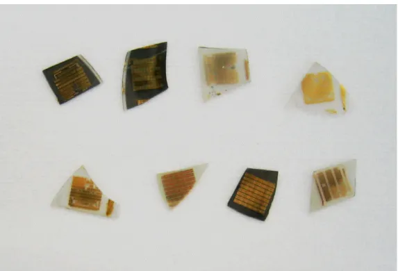
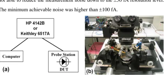
(a) Schematic of a completed AlGaN MSM photodiode. (b)-(d) Microphotographs of MSM devices with different finger width/spacings……….. (a)-(c) SEM pictures of the fabricated AlGaN MSM devices…………. SEM pictures of AlGaN MSM photodiode sample: interdigitated metal finger structures………... Completed AlGaN photodiode samples which are ready for characterization……… (a) Schematic of spectral reflectivity measurement setup. (b) A photograph of the experimental setup……….. (a) Schematic of spectral transmission measurement setup. (b) A picture of the experimental setup………. (a) Schematic of I-V measurement setup (b) A picture of the probe station used for on-wafer I-V measurements………...
65 66 67 67 69 69 70 70 72 73 74
5.4 5.5 5.6 6.1 6.2 6.3 6.4 6.5 6.6 6.7 6.8 6.9
(a) Schematic of spectral photoresponse measurement setup (b) Picture of the experimental apparatus……….. Schematic of UV high-speed pulse response measurement (a) 359 nm setup (b) 267 nm setup. (c) Photograph of 267 nm high-speed setup. Inset shows the microwave probe station, microwave probes, UV optics, and DUT………... Schematic diagram of the low-frequency noise characterization setup... (a) Spectral reflectivity measurement of GaN Schottky photodiode wafer. (b) Spectral transmission curve of the same detector wafer……. (a) Spectral reflectivity measurement of thin Au and ITO films (b) Transmission spectrum of the deposited Au and ITO films……… Absorption spectrum of thin Au and ITO films. Inset shows the UV absorption spectrum………. (a) Measured I-V curves for GaN Schottky photodiodes. (b) Corresponding semi-log plot of I-V data………. (a) Spectral quantum efficiency for GaN Schottky photodiodes. (b) Corresponding spectral responsivity curves……… Measured temporal pulse response of an 80 µm diameter GaN ITO-Schottky photodiode……… Measured and simulated spectral reflectivity of the AlGaN RCE photodiode wafer………. (a) I-V curves of AlGaN RCE Schottky photodiodes samples (b) Dark current density of a 100×100 µm2 RCE ITO-Schottky photodiode…….
Measured spectral quantum efficiency of Au and ITO-Schottky RCE 76 78 80 82 83 84 85 86 87 88 89
6.10 6.11 6.12 6.13 6.14 6.15 6.16 6.17
photodiodes. Inset shows the corresponding spectral responsivity curves………... Pulse response of a 150×150 µm2 Au-Schottky RCE-PD as a function
of reverse bias. Inset shows the area dependence of pulse responses….. Pulsewidth variation with device area under 357 nm and 267 nm illumination. (a) Au-Schottky photodiode (b) ITO-Schottky photodiode……… Normalized pulse responses of 30 µm-diameter Au and ITO-Schottky RCE photodiodes with 77 ps and 154 ps FWHM respectively. Inset shows the corresponding FFT curves……….. (a) I-V curves obtained from AlGaN Au-Schottky photodiodes with different device areas (b) Dark current measurement of a 150×150 µm2
device. Inset shows the dark current density for the same device……... Dark current density of a 100x100 µm2 solar-blind ITO-Schottky photodiode. Inset shows the linear I-V curve of another 100x100 µm2
device………... Dark current of a 30 µm diameter solar-blind AlGaN Schottky photodiode measured with Keithley 6517A electrometer. The inset shows the same plot in logarithmic scale………. I-V curves of solar-blind AlGaN Schottky detectors with different device areas (a) Linear scale. (b) Logarithmic scale……… (a) Measured spectral responsivity of the AlGaN Au-Schottky photodiode as a function of reverse bias. (b) Zero bias spectral
90 92 93 94 96 97 98 99
6.18 6.19 6.20 6.21 6.22 6.23 6.24 6.25
quantum efficiency of a solar-blind Au-Schottky device……… Bias dependent spectral responsivity of solar-blind AlGaN ITO-Schottky photodiodes, measured at room temperature. In the inset, the corresponding external quantum efficiency curves are plotted………... (a) Linear plot of I-V data and exponential fit for a 30 µm diameter AlGaN Au-Schottky detector. (b) Calculated differential resistance for the same device……… (a) High-speed pulse response of a 30 µm diameter Au-Schottky device as a function of applied reverse bias. (b) Corresponding FFT curves of the temporal data……….. (a) Normalized pulse response data for AlGaN Au-Schottky detectors with different areas. (b) Corresponding frequency response curves…… Second-order exponential fitting to the decay part of pulse response obtained with (a) 30 µm diameter device. (b) 60 µm diameter device… (a) Temporal pulse response of a 60 µm diameter AlGaN ITO-Schottky photodiode taken at -13 V bias. Inset shows the calculated frequency response of the temporal data………. (a) Low-frequency spectral noise measurements of a high-leakage 80 µm diameter Schottky photodiode as a function of applied reverse bias. (b) Noise power density of the same device at 1 Hz as a function of reverse bias……….. (a) Dark current density of an MSM photodiode with 10 µm finger spacing. Inset shows the leakage current in logarithmic scale. (b) I-V curves of a device with 5 µm finger spacing under different
100 101 102 103 104 106 107 108
6.26 6.27 6.28 6.29 6.30 6.31 6.32 illumination conditions……… (a) Measured spectral responsivity curves of AlGaN MSM photodiodes as a function of bias voltage. (b) Linear-scaled plot of the corresponding spectral quantum efficiency under 2 V bias………. (a) Bias-dependent temporal pulse responses of an AlGaN MSM photodiodes with 3 µm finger spacing. Inset shows the measured FWHM values with respect to bias voltage. (b) Corresponding FFT curves………... (a) Dark current of a 100x100 µm2 solar-blind AlGaN p-i-n photodiode. The inset shows the same plot in logarithmic scale. (b) Dark current density before/after recess etch and UV photocurrent obtained from the same device……… (a) Spectral quantum efficiency and the corresponding responsivity curve of the non-etched AlGaN p-i-n photodiode. (b) Spectral responsivity as a function of recess etch of the p+ GaN cap layer…….. Exponential curve fitting to the measured dark current of a 100x100 µm2 AlGaN p-i-n device. Inset figure shows the reverse and forward
bias part fitting curves separately in a semi-log plot………... (a) Bias dependent pulse response of a 30 µm diameter AlGaN p-i-n photodiode before recess etch. Inset shows the FFT of temporal data. (b) Normalized pulse response of the same device after recess etch. The corresponding frequency response is shown in the inset figure…... (a) Normalized pulse response measurements of the AlGaN p-i-n photodiode before and after recess etch. (b) Curve fitting to the pulse
110 111 112 114 115 116 117
6.33 6.34
6.35
6.36
response of the recess etched device……… Transmission spectrum of Al0.6Ga0.4N MSM photodiode wafer……….
(a) I-V measurement of Al0.6Ga0.4N MSM photodiode. (b) Dark
current measurement upto 300 V bias. Inset shows the semilog plot….. Spectral quantum efficiency of Al0.6Ga0.4N MSM photodiode. Inset
shows the corresponding responsivity curve………... Measured pulse response of a 3 µm Al0.6Ga0.4N p-i-n device. Inset
shows the corresponding calculated FFT curve………... 118 120
121
121
List of Tables
2.1 2.2 3.1 3.2 3.3 3.4 3.5 3.6 6.1 6.2 6.3 6.4Reported best performances for AlxGa1−xN-based visible-blind
photodiodes………... Reported best performances for AlxGa1−xN-based solar-blind
photodiodes………... Epitaxial layer structure of homojunction GaN Schottky photodiode……….……... Epitaxial structure of heterostructure AlGaN RCE Schottky photodiode Epitaxial structure of solar-blind AlGaN Schottky photodiode………... Solar-blind AlGaN MSM photodiode structure………... Epitaxial structure of solar-blind AlGaN p-i-n photodiode……….. Solar-blind Al0.6Ga0.4N MSM photodiode structure……….
Bias dependent high-speed characteristics of Schottky photodiodes…... Device area dependent high-speed characteristics of solar-blind AlGaN Au-Schottky photodiodes………. I-V characteristics of fabricated AlGaN photodiode samples………….. Spectral photoresponse characteristics of fabricated AlGaN photodiode samples………. 40 41 44 45 46 47 48 49 104 105 124 125
6.5
6.6
Detectivity and noise characteristics of fabricated AlGaN photodiode samples………. High-speed pulse response characteristics of fabricated AlGaN photodiode samples………..
126
CHAPTER 1. INTRODUCTION
Chapter 1
Introduction
The ultraviolet (UV) region of the electromagnetic spectrum covers the wavelengths between 400 nm (3.1 eV) and 10 nm (124 eV). The most important natural UV source is the Sun. Solar UV radiation corresponds to 9% of the total energy outside the Earth’s atmosphere. However (and fortunately), the stratospheric ozone layer prevents the highly ionizing radiation with wavelengths shorter than 280 nm to reach the Earth’s surface [1]. In 1999, the U. S. Air Force published a study which identified the solar-blind wavelength cutoff as 280 nm, based on a series of solar UV emission and atmospheric transmission measurements [2]. This served to define the solar-blind region, the spectral range where the background UV radiation is absent. Likewise, the spectrum covering the wavelengths shorter than 400 nm is defined as the
visible-blind region, as human eye responds to radiation within 400-760 nm.
Generation and detection of optical UV signals are of great importance for a wide range of applications. At the generation side, UV (blue) light emitters are/can be used in full-color/projection displays, high-density optical storage systems, UV lithography, sterilization of biological and chemical agents, covert space-to-space communications, etc. Detection of UV radiation is vital for applications in a number of broad areas, including scientific research,
CHAPTER 1. INTRODUCTION
applications. Some of these applications are fire alarms (flame detection), combustion and engine monitoring systems, environmental (ozone layer) monitoring, detection of biological and chemical agents, missile plume detection and early threat warning systems, secure inter-satellite communications, and underwater/sub-marine communication systems [1], [3].
Traditionally, UV detection has been accomplished by photomultiplier tubes (PMTs), thermal detectors, and narrow-bandgap semiconductor photodiodes [4]. PMTs exhibit high gain and low noise, and can be fairly visible-blind. However, they are expensive, bulky, and physically fragile. In addition PMTs require high operation voltages (usually > 1 kV), and they are susceptible to magnetic fields. In order to achieve solar-blind detection, PMTs should be integrated with complex and expensive filters. Thermal detectors (pyrometers and bolometers) generally are used for calibration in the UV range. Although they are useful as radiometric standards, these detectors are slow and their response is wavelength independent.
Semiconductor photodetectors are small, lightweight, insensitive to magnetic fields, and they do not require high voltage sources. Their low cost, good linearity and sensibility, and capability for high-speed operation make semiconductor detectors an excellent approach for UV detection. Due to its well-established technology, silicon (Si) is the semiconductor most commonly used for UV photodiodes. The main problem for Si devices (and other narrow-bandgap detectors) is device aging, due to absorption of radiation with energy much higher than the semiconductor bandgap. Similar to PMTs, Si detectors also demand costly filters for true visible/solar-blind operation.
The use of wide-bandgap semiconductors makes it possible to avoid filters and reduces aging effects. Moreover, wide-bandgap materials are chemically and thermally more stable, which is an advantage for harsh operation
CHAPTER 1. INTRODUCTION
conditions (under high power and high temperature levels). These semiconductors are diamond, SiC, III-nitrides, and wide-bandgap II-VI materials. III-nitrides (i.e. AlN, GaN, InN, and their ternary compounds) present several important advantages over other wide-bandgap semiconductors:
• High absorption coefficients and sharper cut-offs, due to their direct bandgap.
• Tunability of the cut-off wavelength by changing the mole fraction of their ternary alloys.
• Capability for heterojunction devices using bandgap engineering. • Intrinsic solar-blindness of AlxGa1−xN ternary alloy for x ≥ 0.38.
With all these advantages, III-nitrides have become the most promising materials for the fabrication of optoelectronic devices in the blue and UV regions of the spectrum [5, 6].
The wide-bandgap AlxGa1−xN ternary alloy is well-suited as a photodetector
material for operation in the wavelength range of 200 nm to 365 nm. Its outstanding material properties make AlxGa1−xN suitable for a variety of harsh
environments. Potential uses of AlxGa1−xN UV photodetectors include military,
space-based, environmental, and industrial applications for which older PMT and Si technology is inappropriate. If properly constructed, AlxGa1−xN-based
photodetectors could offer significant advantages over PMT detectors in terms of size, cost, robustness, complexity, dark current, bandwidth, and solar-blind operation.
The motivation behind this work is the need for high-performance, solid-state UV photodetectors that can be cost-effectively manufactured into high-density arrays. Our aim was to develop high-performance UV detectors using
CHAPTER 1. INTRODUCTION
AlxGa1−xN material system and to make contributions to the device
performance of UV photodiodes.
During this work, research was carried out on six different AlxGa1−xN
photodiode structures. Two of them were designed for visible-blind operation, whereas four structures were designed for true solar-blind detection. Three types of photodiode structures were utilized: Schottky, metal-semiconductor-metal, and p-i-n.
Epitaxial growth of the designed detector structures was accomplished by semiconductor wafer growth companies and universities abroad. All fabrication and characterization processes were done at Bilkent University. The detector samples were fabricated in Advanced Research Laboratory (ARL) class-100 cleanroom facility of Physics Department. Testing of the fabricated samples was done in the class-10000 cleanroom of ARL. High-speed testing of the photodiode samples was accomplished in the Optics Laboratory of Electrical & Electronics Engineering Department.
In Chapter 2, basic background information is presented. Operation principles, types, and basic characteristics of photodiodes are introduced. Growth and material properties of AlxGa1−xN material system are summarized.
At the end of this chapter, an overview of AlxGa1−xN based photodiode
research is given.
Detector design issues are presented in Chapter 3. Scope of design and AlxGa1−xN epitaxial structures are described. The fabrication process of UV
photodiode samples is explained in detail in Chapter 4. Basic process techniques for III-nitride device processing is followed by a step-by-step description of device fabrication. Chapter 5 is devoted to the presentation of
CHAPTER 1. INTRODUCTION
characterization methods and experimental setups. Information about the characterization tools is also given.
The measurement results of the completed UV photodiode samples are presented in Chapter 6. The characterization results of each detector sample are presented in a separate section. At the end of the chapter, the samples are compared in terms of device performance. The thesis concludes with a summary of achievements, future research directions, and a list of publications that resulted from this work.
CHAPTER 2. BACKGROUND
Chapter 2
Background
A photodiode is basically a radiation-sensitive semiconductor diode. The diode structure is formed with either a p-n junction or a metal-semiconductor contact. When operated under reverse bias, it produces an electrical current (photocurrent) proportional to the incident optical field. Photogenerated electrons and holes drift in the opposite directions. Such a transport process induces an electric current in the external circuit [7]. In this chapter, we first present the fundamental background information for photodiodes: basic photodiode operation mechanism, types of photodiodes, their operation principles, and photodiode characteristics. Afterwards, material issues and characteristics of AlGaN material system are summarized. Finally, an overview of AlGaN-based UV photodiode research literature is given.
2.1 Photodiode Operation
A photodiode consists of a semiconductor with two electrical contacts: anode and cathode. Figure 2.1 summarizes the basic operation of a photodiode. Incident photons with energy higher than the bandgap energy of the semiconductor have a certain probability to be absorbed within the semiconductor layer. Such a successful absorption process results in the
CHAPTER 2. BACKGROUND
generation of a free electron-hole pair. If a reverse bias voltage is applied to the contacts so that anode has a lower potential than cathode, an electric field builds up across the semiconductor. The photogenerated carriers drift towards the contacts under this electric field. Electrons and holes drift in the opposite directions: electrons towards the cathode, holes towards the anode. Such a transport process induces an electric current in the external circuit, which is the photocurrent. Hence, the photodetection event in a photodiode can be summarized in a three-step process:
• Absorption of photons in the semiconductor and generation of carriers • Drift of carriers under the local electric field
CHAPTER 2. BACKGROUND
2.2 Types of Photodiodes
Depending on the type of contacts and diode structure, several types of photodiodes exist including Schottky (barrier) photodiode, metal-semiconductor-metal (MSM) photodiode, p-i-n photodiode, avalanche photodiode, and phototransistors [8]. The latter two photodiode structures feature internal gain, whereas Schottky, MSM, and p-i-n photodiodes display no internal gain mechanism.
2.2.1 Schottky Photodiode
A Schottky photodiode consists of a semiconductor with two different metal-semiconductor contacts: a linear ohmic contact and a rectifying Schottky contact. The rectifying Schottky junction forms a potential barrier, which creates a depletion region within the semiconductor. This behavior is very similar to the one-sided abrupt p+-n junction. When the diode is reverse biased, the incident radiation generates electon-hole pairs within the depletion region near the metal where they are collected efficiently and rapidly by the built-in field. Schottky photodiodes are unipolar devices with only one type of impurity dopant. Most widely, n-type semiconductors are utilized to benefit from the higher mobility of electrons and better material properties of n-type semiconductors.
Figure 2.2 shows a schematic diagram of a typical n−/n+ Schottky photodiode structure. The Schottky metal is deposited on the lightly doped (n−) semiconductor, whereas the low-resistance ohmic contact is formed on the highly doped (n+) semiconductor layer. The depletion width depends on the doping level of n− layer and applied reverse bias voltage. To eliminate the
CHAPTER 2. BACKGROUND
diffusion current originating from low-field (non-depleted) regions, whole n− layer (d) should be depleted. In this case, all photogenerated carriers will drift towards the contact regions.
Fig. 2.2: Schematic cross-section of an n-/n+ Schottky photodiode.
No minority carrier diffusion/injection process exists in this device. Therefore, Schottky photodiodes are known as majority carrier devices. This property makes Schottky photodiodes attractive for applications where high-speed detection is needed. In addition, when compared with bipolar devices (i.e., pn-junctions, p-i-n structures, etc.), Schottky photodiodes are easier to grow and fabricate. Challenging difficulties are faced during the growth and process of p-type semiconductor layers and p-type ohmic contacts respectively. In terms of photoresponse, Schottky photodiodes suffer from low efficiency, mainly due to the highly absorptive and reflective metal Schottky layer. This drawback can be solved by using transparent contact material or utilizing a more complex back-illuminated heterostructure design.
CHAPTER 2. BACKGROUND
2.2.2 Metal-Semiconductor-Metal Photodiode
An MSM photodiode is a unipolar device with two back-to-back Schottky junctions formed on the same semiconductor surface. Under the application of a bias voltage, one of the diodes becomes reverse biased, forming a depletion region that will tend to sweep out photocarriers. The other diode becomes forward biased, allowing the collected photocurrent to flow out just as an ohmic contact. Under sufficiently high bias voltage, the depletion region extends and touches the small space-charge region under the forward biased electrode.
(a) (b) Fig. 2.3: (a) Cross-section of an MSM photodiode. (b) Top view of the
interdigitated MSM structure.
Figure 2.3 shows the schematic cross-section and top-view drawings of a typical MSM photodiode. The Schottky metal contacts are deposited on a single undoped semiconductor. To minimize the carrier transit time, Schottky electrodes are deposited in form of interdigitated fingers. This geometry also increases the carrier collection efficiency by maximizing the effective depletion area. Light is coupled to the device from the top surface, thereby
CHAPTER 2. BACKGROUND
allowing photons to penetrate into the active layer in the region between the electrode fingers. Photogenerated electron-hole pairs are swept out of the contacts by the electric field, thus contributing to the photocurrent.
Interdigitated MSM photodiodes are simple to realize. Both growth and fabrication processes are straight forward. No ohmic contacts are needed. Especially, the fabrication of MSM photodiodes is quite simple and compatible with integrated circuit processing. The interdigitated device structure leads to very small capacitance values, which is important for high-speed operation. The use of two rectifying (blocking) contacts significantly reduces the dark current of the photodiode. However, device efficiency is low due to the shadowing effect of metal electrodes. This may be alleviated through backside illuminated device structure. Another possible solution is to use transparent conductor or thin semitransparent metal electrodes.
2.2.3 P
−I−N Photodiode
A p-i-n (p-intrinsic-n) photodiode has heavily doped p- and n-type regions separated by an intrinsic (undoped or compensated) region, which is the major absorption layer. Two ohmic contacts are formed at the p- and n-type regions. When reverse bias is applied to the contacts, a constant and uniform electric field builds up within the intrinsic region. Photogenerated carriers are separated by the electric field and contribute to the external photocurrent by drift process. The schematic of a typical p-i-n photodiode is shown in Fig. 2.4. The key feature of the p-i-n structure is that most carrier generation occurs in the high electric field region and transport of carriers is dominated by the drift process. This results in both high efficiency and high-speed performance. However, depending on the device structure and type of illumination, a portion of incident radiation can be absorbed within the non-transparent contact regions.
CHAPTER 2. BACKGROUND
In such cases, the device efficiency and bandwidth performance will be degraded by the diffusion of carriers generated in the contact layers.
Fig. 2.4: Drawing of a typical p-i-n photodiode
Compared to Schottky and MSM photodiodes, p-i-n photodiodes have several important advantages. The thickness of absorption layer is determined by the geometry, not by the bias voltage. Even under low reverse bias, efficient carrier generation and collection are obtained. Since the electric field in the i-layer is constant, the intrinsic speed of response is optimized. Moreover, the reverse dark current is nearly independent of bias voltage. The diffusion component of the photocurrent can be eliminated by a heterostructure p-i-n design with transparent contact regions. The main expense for p-i-n photodiodes comes from the growth and fabrication side. Growing high-quality
p-type semiconductor layers and making high-quality, low resistance p-type
CHAPTER 2. BACKGROUND
2.2.4 Avalanche Photodiode and Phototransistor
Avalanche photodiodes and phototransistors are semiconductor-based photodiodes with internal gain mechanisms. These devices are attractive for a number of applications where the incident optical signal is very weak or where high electrical output is desired. An avalanche photodiode consists of a reverse biased p-n junction that is operated at voltages close to the breakdown [7]. Due to the intense electric field, photogenerated carriers in the depletion region travel at their saturation velocity. These high-energy carriers may produce secondary electron-hole pairs by ionizing collisions with the lattice. These new electrons and holes again drift in opposite directions, and all or some of them may produce new carriers. This process is known as impact ionization, and leads to carrier multiplication and gain.
A phototransistor is a photodiode which provides internal gain via transistor action. This device is simply equivalent to a transistor with a photodiode connected across base and collector, and acting as a current generator not different than the reverse collector-base current. In a bipolar phototransistor, the reverse-biased base-collector junction operates as a p-n junction photodiode, and its photocurrent is amplified by the transistor gain mechanism. Similarly, unipolar field effect phototransistors provide large internal gain. They are the photosensitive counterparts of field effect transistors.
The price paid for the internal gain-assisted photoresponse performance is the increased complexity in the design, growth, and fabrication process. A requisite for proper device operation is high-quality material growth with low defect density.
CHAPTER 2. BACKGROUND
2.2.5 Comparison of Photodiode Types
When the advantages and drawbacks of the photodiode types are compared, one can safely claim that the photodiodes with internal gain mechanism (avalanche photodiodes and phototransistors) have the most complex structures. The large gain-assisted photoresponse and high sensitivity performance comes at the expense of increased cost due to challenging growth and fabrication processes. Since these devices are not in the scope of this thesis, a qualitative comparison between the other three photodiode structures (Schottky, MSM, and p-i-n photodiodes) would be useful.
• Complexity (Cost): Bipolar p-i-n structures are more complex to grow and fabricate since they require layers with two different types of impurity doping. In most material systems, n-type doping is not a problem, while in a number of material systems (especially those which are in the development phase, like AlxGa1−xN) high-quality p-type layer
growth and low-resistance p-type ohmic contact process are still challenging issues. Unipolar Schottky and MSM photodiodes are easily grown with one type of doping, which is mostly n-type. MSM photodiodes own the simplest fabrication process without ohmic contacts. Hence, regarding the complexity and cost in growth and fabrication process, MSM devices are the simplest and cheapest, p-i-n devices are the most complex and expensive ones.
• Photoresponse: In terms of photoresponse or device efficiency, conventional vertically front-illuminated MSM and Schottky photodiodes suffer from the optical loss in metallic Schottky contacts. This loss can be decreased by using very thin (<100 Å) semitransparent metallic contacts. Complete elimination of this loss may be possible by
CHAPTER 2. BACKGROUND
the use of non-metallic, highly transparent conducting materials. Another alternative solution is to change the illumination scheme. Back-illuminated (from the substrate side) Schottky and MSM photodiodes can have thick Schottky metals on their top surface however the substrate and intermediate device layers should be transparent at the operation wavelength. Back-illuminated heterojunction structures can overcome the low efficiency problem for Schottky and MSM photodiodes. For vertically illuminated p-i-n photodiodes, similar arguments are valid due to the optical absortion in low field, quasi neutral (p- or n- type) regions. The device efficiency can be maximized by using heterojunction designs with transparent/window (larger bandgap) layers in contact regions.
• Speed: Obviously, unipolar majority carrier devices have the advantage of the non-existing minority carrier injection and diffusion. Therefore, it is expected that Schottky and MSM photodiodes have better high-speed characteristics when compared to p-i-n counterparts. However, with clever heterojunction device design, the diffusion current in p-i-n photodiodes could be minimized and excellent high-speed performance can be achieved.
• Surface Effects: The quality of Schottky junctions strongly depends on the properties of the semiconductor surface. Surface states, surface defects, and external particles like thin oxide layers have negative effect on the quality of Schottky contacts. The device performance of Schottky and MSM photodiodes are directly affected by surface properties. Therefore, it is harder to get uniform performance with these devices. The contact quality of p-i-n photodiodes depends dominantly on the quality of doping and contact metallization/annealing process. For
CHAPTER 2. BACKGROUND
uniform and reliable device performance p-i-n photodiodes are more preferable.
2.2.6 Alternative Photodiode Structures
Conventional photodiodes are vertically illuminated. The light is incident either from the front side or back (substrate) side (Fig. 2.5). In either case, the photons are absorbed within the active absorption layer as they travel through the device structure. Thicker absorption layer means more photogeneration and higher efficiency performance. However, at the same time, this results in longer carrier transit times, which makes the detector response slower. On the other hand, if we design a vertically illuminated photodiode with a thin absorption layer, we obtain faster response but lower efficiency. This effect is known as the “bandwidth-efficiency trade-off” and limits the maximum achievable bandwidth-efficiency product from a conventional vertically illuminated photodiode.
(a) (b) Fig. 2.5: Conventional vertically illuminated p-i-n photodiodes. (a)
CHAPTER 2. BACKGROUND
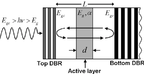
Mainly two alternative photodiode structures have been offered to solve this trade-off: edge-coupled (side-illuminated) photodiodes and resonant-cavity-enhanced (RCE) photodiodes [9].
Fig. 2.6: Edge-coupled (side-illuminated) p-i-n photodiode structure
Edge-Illuminated Photodiodes: Light is incident horizontally from the edge
(side) of the photodiode. Figure 2.6 shows the schematic of an edge-illuminated p-i-n photodiode. By changing the illumination direction, the dependence of efficiency and time response are de-coupled. Absorption of incident photons takes place along the horizontal direction whereas the photogenerated carriers travel to the contact regions in the vertical direction. Hence, absorption and time response will be proportional to the lateral width (L) and thickness (d) of the active layer, respectively. With such a device structure, one can optimize the efficiency and speed performance independently. This advantage comes at the expense of more complex design, fabrication, and particularly packaging process. Efficient coupling of the incident light into the sub-micron absorption layer is a challenging task but not impossible. Using
CHAPTER 2. BACKGROUND
edge-illuminated design, very high bandwidth-efficiency performance were reported by several research groups [10]−[12].
RCE Photodiodes: Another alternative approach for solving the
bandwidth-efficiency trade-off was introduced in early 90’s [13], [14]. The suggested detector structure consisted of a conventional vertically illuminated detector placed inside a Fabry-Perot micro-cavity. The idea was to enhance the absorption at resonance frequencies of the micro-cavity. Photons at resonance wavelength will be recycled within the detector cavity, thereby making multiple passes through the absorption layer. Hence, the effective absorption layer thickness will be increased which results in enhanced absorption and efficiency. The photon recycling process does not affect the high-speed performance of the detector since the photon round-trip times are much shorter than carrier transit times. Therefore, using a low-loss cavity and a thin active layer, both high efficiency and high bandwidth performance can be achieved [15].
Fig. 2.7: Schematic of an RCE photodetector operation. Top and bottom Bragg mirrors are centered at the operation (resonance) wavelength.
CHAPTER 2. BACKGROUND
A schematic drawing of an RCE photodiode is shown in Fig. 2.7. The mirrors of the resonant cavity are formed with highly-reflecting Bragg mirrors centered at the desired operation (resonance) wavelength. One should remember that the resonant-cavity enhancement effect enhances the device efficiency only at the resonance wavelengths. Indeed, the efficiency at off-resonance wavelengths is suppressed below the single-pass (conventional) device efficiency. The wavelength selectivity of RCE photodiodes may be useful for applications where wavelength selective detection is desired. The cost of this approach is the increased device complexity. Precise growth is required for the desired enhanced performance. Successful RCE photodiodes with high bandwidth-efficiency performance have been demonstrated using several material systems [16]−[23].
2.3 Photodiode Characteristics
The performance of photodiodes is measured with common detector parameters: current-voltage, quantum efficiency and responsivity, bandwidth and time response, noise and detectivity [7], [8], [24]−[26]. These parameters represent the main electrical and optical characteristics of the photodiode.
2.3.1 Current-Voltage
Current-voltage (I-V) characteristic of a photodiode is determined by the current transport processes in the diode junction. Different current transport mechanisms are dominant for photodiodes based on metal-semiconductor junctions (Schottky and MSM photodiodes) and p-n junctions (p-i-n photodiode).
CHAPTER 2. BACKGROUND
For Schottky and MSM photodiodes, the junction current is dominated by the thermionic emission of majority carriers over the Schottky barrier, which is given by * 2 exp q b exp qVA 1 J A T kT nkT φ − ⎡ ⎤ ⎛ ⎞ ⎛ ⎞ = ⎜ ⎟ ⎢ ⎜ ⎟− ⎥ ⎝ ⎠ ⎝ ⎠ ⎣ ⎦, (2.1) where * 2 * 3 4 qm k A h π
= is known as the Richardson constant, φb is the Schottky
barrier height, VA is the applied bias voltage, and n (≥1) corresponds to the
ideality factor of the diode. If we write the diode current as
0 exp 1 A qV I I nkT ⎡ ⎛ ⎞ ⎤ = ⎢ ⎜ ⎟− ⎥ ⎝ ⎠ ⎣ ⎦, (2.2)
I0 is the reverse saturation current. In forward bias regime (VA>0), I increases
exponentially with VA. Under reverse bias (VA<0), I becomes equal to the
reverse saturation current, I0. The ideality factor of an ideal Schottky diode is 1.
Non-ideal n>1 values can be observed due to surface effects like interfacial layers, barrier height inhomogeneity, or image-force lowering effect.
By analyzing the forward current of a Schottky photodiode, one can determine diode parameters including the reverse saturation current, barrier height, ideality factor, and series resistance. I0 and φb can be found by
extrapolating the forward current towards V=0. n is determined by the slope (dV/dI) of the forward I-V curve. The series resistance effect appears as a roll-off in the forward current, where the photodiode operates in the high-level injection regime. The series resistance can be calculated by the slope of the (dV/dI)I versus I plot.
The reverse current of the Schottky photodiode is the leakage or dark current of the detector. Since photodiodes are operated under reverse bias, this
CHAPTER 2. BACKGROUND
is the current flowing through the photodiode under the absence of illumination. Ideally, this value is equal to the reverse saturation current. Taking image-force lowering effect into consideration, we obtain a more-accurate voltage dependent expression for the reverse photodiode current:
(
)
1/ 2 2 0 0 2 exp D i A n C qN V b Aq D N q I kT kT φ φ κε − ⎡ ⎤ ⎛− ⎞ = ⎢ ⎥ ⎜ ⎟ ⎝ ⎠ ⎣ ⎦ , (2.3)where A is the active device area, Dn, Nc, Nd, φi depend on material properties.
It is desired to have the leakage current as low as possible. Another reverse bias detector characteristic is the reverse bias breakdown voltage. This is the voltage where the diode begins to conduct very large currents due to avalanche or zener breakdown process. It strongly depends on the material quality and the bandgap of the semiconductor. Breakdown voltage determines the maximum operating voltage of the photodiode.
For MSM photodiodes, reverse saturation current flows through the back-to-back Schottky junctions. Similar to Schottky photodiodes, thermionic emission current is dominant. However, unlike a single Schottky junction, both electron and hole current components have to be considered, and the dark current density has the general expression,
* 2 * 2 exp bn exp bp n p q q J A T A T kT kT φ φ ⎛− ⎞ − ⎛ ⎞ = ⎜ ⎟+ ⎜ ⎟ ⎝ ⎠ ⎝ ⎠. (2.4)
The dark current of a p-i-n photodiode is the sum of the diffusion current and the recombination/generation current within the intrinsic layer. The total current density flowing through the photodiode can be written as
2 2 exp 1 exp 1 2 2 p i n i A i A p D n A qD n qD n qV qWn qV J L N L N kT τ kT ⎛ ⎞ ⎡ ⎛ ⎞ ⎤ ⎡ ⎛ ⎞ =⎜⎜ + ⎟⎟⎢ ⎜ ⎟− +⎥ ⎢ ⎜ ⎟− ⎤ ⎝ ⎠ ⎝ ⎠ ⎥ ⎣ ⎦ ⎣ ⎝ ⎠ ⎦, (2.5)
CHAPTER 2. BACKGROUND
where W is the width of depletion region, Dn,p and ND,A are the diffusion
constants and doping concentrations of n- and p-type regions, respectively. Since the n+ and p+ layers sandwiching the intrinsic layer are heavily doped,
ND and NA are high and the diffusion current (the first term in Eq. (2.4)) is
usually negligible. Hence, recombination/generation current dominates the diode current. The forward current increases exponentially with an ideality factor of 2, which is a characteristic of recombination current. In reverse bias regime, the same term dominates as generation current. Hence, the reverse (dark/leakage) current in an ideal p-i-n photodiode is governed by
2 i gen qAWn I I τ = = − , (2.6)
Comparing the current equations of Schottky and p-n junctions, the current mechanisms are entirely different: thermionic emission current for Schottky diodes, recombination/generation current for p-i-n diodes. However, the I-V characteristics both in forward and reverse bias regime are very similar: exponentially increasing forward current and almost constant reverse current. In comparison with Schottky photodiodes, the p-n junction photodiodes indicate some important advantages. The thermionic emission process in Schottky barrier is much more efficient than the diffusion process and, therefore, for a given built-in voltage, the saturation current in a Schottky diode is several orders of magnitude higher than in the p-n junction. In addition, the built-in voltage of a Schottky diode is smaller than that of a p-n junction with the same semiconductor.
2.3.2 Quantum Efficiency and Responsivity
The quantum efficiency of a photodiode is defined as the probability that a single photon incident on the detector generates an electron-hole pair that
CHAPTER 2. BACKGROUND
contributes to the photocurrent. For a conventional vertically illuminated photodiode, the spectral quantum efficiency can be written as
(
)
( ) (1 R) 1 exp ( )d
η λ = − ⎡⎣ − −α λ ⎤⎦ (2.7) where R is the reflectivity of the front surface, α(λ) is the absorption coefficient, and d is absorption layer thickness. η is proportional with absorption layer thickness. However, larger d results in longer transit times and slower detector response. This effect is known as the bandwidth-efficiency trade-off. η drops rapidly for wavelengths larger than bandgap wavelength (λ>hc/Eg) since the
photon energy becomes insufficient for photogeneration.
Responsivity is another measure of the detector response. It relates the photocurrent to the incident optical power, and is expressed as
( ) ( ) 1.24 p i e m R P h η λ µ λ η ν = = = (2.8)
Responsivity has the units of A/W. To maximize the responsivity or quantum efficiency of the photodiode, the surface reflectivity should be minimized. For Schottky photodiodes, this can be satisfied by using thin metallic contacts, whereas for p-i-n photodiodes, the reflectivity of semiconductor/air interface can be minimized with a proper anti-reflection coating. In addition, the absorption in Schottky contact material and the absorption in p+ or n+ layers should be taken into account as additional losses for Schottky and p-i-n photodiodes respectively. For interdigitated MSM photodiodes, the quantum efficiency can be expressed as
(
)
( ) S (1 R) 1 exp ( )d
S W
η λ = − ⎡⎣ − −α λ ⎤⎦
CHAPTER 2. BACKGROUND
where S is the interdigitated electrode spacing and W is the electrode (finger) width. For maximum responsivity performance, smaller electrodes and smaller electrode spacing should be utilized.
Quantum Efficiency of RCE Photodiodes: Assuming that all cavity layers
except the absorption layer (α, d) are transparent at operation wavelength, the quantum efficiency of an RCE photodiode can be calculated by the following equation [15]: 2 1 2 1 2 1 2 1 2 (1 ) (1 )(1 ) 1 2 cos(2 ) d d RCE d d R e R e R R e kL R R e α α α α η φ φ − − − − ⎧ + ⎫ ⎪ ⎪ =⎨ ⎬× − + + + ⎪ ⎪ ⎩ ⎭ − − . (2.10)
R1 and R2 correspond to the top and bottom mirror reflectivity coefficients
respectively. φ1andφ2 are the mirror phase shifts, and L is the total cavity length (Fig. 2.7). The overall efficiency is equal to the conventional efficiency term (1−R1)(1−e−αd) multiplied by the following enhancement factor:
2 2 1 2 1 2 1 2 (1 ) 1 2 cos(2 ) d d d R e enhancement R R e kL R R e α α φ φ α − − − + = − + + + . (2.11)
This term is maximized under resonance condition which is satisfied for
1 2
2kL+ +φ φ =2m mπ, =1, 2,...wherek 2π
λ
= . The optimum RCE condition is
achieved if the condition
2
1 2
d
R =R e−α (2.12)
holds. Using these four design parameters (R1, R2, α, d) one can design the
RCE detector for maximum bandwidth-efficiency performance. Figure 2.8 shows the simulated spectral quantum efficiency of an RCE photodiode with
0.1
d
CHAPTER 2. BACKGROUND
reflectivity. An enhancement factor of ~20 is obtained at resonance wavelengths with R2 =0.99.
Fig. 2.8: Simulated quantum efficiency spectrum of an RCE photodiode as a function of bottom mirror reflectivity, R2.
2.3.3 Bandwidth and Time Response
The response speed of a photodiode depends is limited by several phenomena: • Drift of photogenerated charges through the depletion region
• Diffusion of charge carriers from the location of their generation to the junction depletion region
• Time constant of RC circuit • Carrier trapping
These factors combine and contribute to reduce the device responsivity at high frequencies. The photodiode bandwidth is defined as the frequency at
CHAPTER 2. BACKGROUND
which the responsivity has dropped to half its value at low frequencies. By defining the time constants as τdrift, τdiff, τRC, and τtrap for drift, diffusion, RC,
and trapping processes, the total time constant for the photodiode can be written as,
2 2 2 2 2
drift diff RC trap
τ =τ +τ +τ +τ . (2.13)
The slowest process determines the device bandwidth. Trapping of charged carriers occurs at the trapping centers (defects) within the semiconductor. This effect may be important for high defect-density material in which it can dominate the time response with long time constants. If the material is of high quality with low defect density, the most serious limitation comes from the RC time constant which is given by
1/ 2 0 2 S T RC R q N AR V ε ε τ = ⎛⎜ ⎞⎟ ⎝ ⎠ , (2.14)
where ε0 and εS are permittivities of the free space and semiconductor,
respectively; A is the surface area; N is the concentration of uncompensated charge carriers; and VR is the applied reverse bias voltage. RT is the total device
resistance which can be written as
(
)
d s L T d s L R R R R R R R + = + + , (2.15)where Rs, Rd, and RL correspond to the series, diode (differential), and load
resistances respectively. To reduce the RC time constant, we can decrease the majority carrier concentration adjacent to the junction, increase VR, decrease
the junction area, or lower either the diode resistance or the load resistance. Except for the application of reverse bias, all of these changes reduce the detectivity. The trade-off between response time and detectivity is then apparent.
CHAPTER 2. BACKGROUND
The diffusion time constant is negligible for majority carrier devices. By using transparent p+/n+ layers, the diffusion current in p-i-n photodiodes can be minimized. The depletion region transit time is equal toτdrift =W /υs, where υs
is the carrier saturation drift velocity in the junction field. Using high-quality material and an optimized device structure with thin active region, small device area, and minimized parasitics, transit time-limited detector bandwidth can be achieved.
2.3.4 Noise and Detectivity
A photodiode generates a photocurrent proportional to the incident photon flux Φ (ip = Φ ). Actually, the device generates a random electric current i whose ηe
value fluctuates above and below its average,i i≡ = Φ . These random p ηe fluctuations are regarded as noise. There are mainly three sources of noise in a photodiode:
• Thermal (Johnson) noise, due to random collisions of carriers with the lattice.
• Shot noise, due to random emission of carriers crossing potential barriers.
• Flicker (1/f) noise, related to the presence of traps in contacts, at the surface or within the semiconductor, as well as to leakage currents and defects. 1/f noise is attributed to fluctuations in the mobility and density of charged carriers.
The corresponding noise currents are denoted as iJ, is, and i1/f respectively and
are expressed as 2 2 2 1/ 4 , 2 , J s d f d d BW B i kT i qI BW i kI W R f = = = , (2.16)
CHAPTER 2. BACKGROUND
where Rd is the differential resistance of the photodiode, Id is the dark current, f
is the frequency, and k is a coefficient that depends on the material and on the geometrical parameters of the diode. From these expressions, it is obvious that there exists a trade-off between bandwidth and noise performance. In general, at high frequencies shot noise is dominant, whereas at low frequencies 1/f noise can be higher. Thermal noise may become significant under elevated operating temperatures and for leaky photodiodes with low diode resistance.
The noise equivalent power (NEP) is the optical power required to generate a photocurrent equal to the noise level. For a photodiode with a responsivity R, the NEP is given by
n
I NEP
R
= , (2.17)
where In is the root mean square value of the total noise current:
2 2 2 2
1/
n n J s f
I = i = i + i + i . (2.18)
The normalized (specific) detectivity, D*, is the most important parameter to characterize the noise performance of photodetectors and is obtained from the relation * 2 D D n A BW R A BW D NEP i = = , (2.19)
where AD is the cross-sectional area of the photodiode, and BW is the detector
bandwidth. The unit of D* is cmHz1/2/W. The value of D* increases as the radiation wavelength and the quantum efficiency increases and as the dark current decreases.
CHAPTER 2. BACKGROUND
2.4 Al
xGa
1−xN Material System
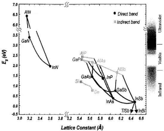
III-Nitride group semiconductors (AlN, GaN, and InN) are known as wide-bandgap semiconductors. They form an important material system because of their direct bandgaps which span the range 1.95–6.2 eV, including the whole visible region and extending well out into the UV range. They form a complete series of ternary alloys which, in principle, makes available any band gap within this range [5], [27]. Figure 2.9 shows the energy bandgap and lattice constant of the common III-V semiconductors and some of the related alloys [28].
Fig. 2.9: Energy bandgap and lattice constant curves for common III-V semiconductor alloys (After Ref. 28).
CHAPTER 2. BACKGROUND
Wide bandgap AlxGa1−xN ternary alloy is particularly important for
optoelectronic applications in the UV portion of the spectrum. Its bandgap energy ranges from 3.4 eV (x=0, GaN) to 6.2 eV (x=1, AlN). This energy range corresponds to the wavelength region of 200-365 nm. This fundamental property essentially makes detectors fabricated from AlxGa1−xN materials
intrinsically blind to photons with wavelengths longer than that of the bandgap of the active layer.
2.4.1 Growth and Material Quality
One of the major disabilities of AlxGa1−xN material system is the lack of
suitable substrate material. Although intense research is underway to produce high-quality bulk GaN or AlN substrates, no native III-nitride substrate is achieved yet. True bulk GaN/AlN crystals have been very difficult to produce because of the extremely high nitrogen pressures involved in their growth [29], [30]. Due to the lack of ideal substrate, AlGaN crystals have been grown on (0001) sapphire (Al2O3) substrates despite its poor structural and thermal match
with AlxGa1−xN layers. The choice of sapphire has been motivated by its low
cost, wide availability in good quality, optical transparency in the visible and UV spectral regions, and its stability at high temperatures. AlxGa1−xN films are
most commonly grown by metal-organic chemical vapor deposition (MOCVD). To achieve smooth films and to accommodate the large lattice mismatch between the nitride semiconductor films and the sapphire substrate, the growth process is initiated with a thin, low-temperature GaN or AlN amorphous buffer layer [31]. The thin buffer layers improve the initial nucleation and enhance the two-dimensional growth. Growth temperatures are very high (900−1100 o