Al
xGa
1−xN-based avalanche photodiodes with high reproducible
avalanche gain
Turgut Tut,a兲 Mutlu Gokkavas, Ayse Inal, and Ekmel Ozbay
Nanotechnology Research Center, Bilkent University, Bilkent, 06800 Ankara, Turkey; Department of Physics, Bilkent University, Bilkent, 06800 Ankara, Turkey; and Department of Electrical and Electronics Engineering, Bilkent University, Bilkent, 06800 Ankara, Turkey
共Received 5 December 2006; accepted 19 March 2007; published online 17 April 2007兲
The authors report high performance solar-blind photodetectors with reproducible avalanche gain as high as 1560 under ultraviolet illumination. The solar-blind photodetectors have a sharp cutoff around 276 nm. The dark currents of the 40m diameter devices are measured to be lower than 8 fA for bias voltages up to 20 V. The responsivity of the photodetectors is 0.13 A / W at 272 nm under 20 V reverse bias. The thermally limited detectivity is calculated as D*= 1.4 ⫻1014cm Hz1/2W−1for a 40m diameter device. © 2007 American Institute of Physics. 关DOI:10.1063/1.2724926兴
The recent developments in high Al-content AlxGa1−xN material growth technology made it possible to fabricate high performance solar-blind photodetectors operating in the ultraviolet共UV兲 spectral region with improved receiver sen-sitivity, low noise, low dark current density, and high speed.1–3 AlGaN-based Schottky, p-i-n, and metal-semiconductor-metal photodetectors with very high perfor-mances have already been demonstrated.4,5The UV-filtering nature of the atmospheric ozone molecules blocks the solar radiation to reach the earth’s surface for wavelengths shorter than 280 nm. In this case, UV photodetectors with cutoff wavelengths around 280 nm, which are also called solar-blind detectors, can detect very weak UV signals under in-tense background radiation. These devices have important applications including missile plume detection, chemical/ biological agent sensing, flame alarms, covert space-to-space and submarine communications, ozone-layer monitoring, and gas detection. Due to their high responsivity共⬎600 A/W兲, high speed, high cathode gain共on the order of a million兲, and low dark current properties, photomultiplier tubes 共PMTs兲 are frequently used in such applications. However, PMTs are very expensive and bulky. Besides, they require a cooling system, and they have high operation voltages in excess of 1000 V. To achieve solar-blind detection, PMTs should also be integrated with complex and expensive filters. In order to avoid these disadvantages, high performance solid-state UV photodetectors with high internal gain are needed.6 Wide band-gap semiconductor photodetectors, such as AlxGa1−xN with x = 0.4, are ideal candidates for this purpose. These de-vices are intrinsically solar blind, in which no additional fil-ters are needed, they have low noise,7 and fast response times.8 The lack of high internal gain has been the major limitation for the usage of AlGaN photodetectors for appli-cations that require high sensitivity detectors. There have been several theoretical research work that examined the avalanche effect in GaN and AlGaN-based structures.9–11 Ex-perimental work on both GaN 共Refs. 12–18兲 and AlGaN-based 共Refs. 4, 19, and 20兲 avalanche photodiodes 共APDs兲 were also reported. However, reproducible high gain in AlGaN-based APDs is still a major limitation. In this letter,
we report the realization of solar-blind AlGaN-based ava-lanche photodetectors with reproducible high avaava-lanche gain. The epitaxial structure of the avalanche photodetector is designed for solar-blind operation with high avalanche gain. The Al0.4Ga0.6N absorption layer was used as a multiplica-tion layer withc= 276 nm. The AlxGa1−xN epitaxial layers of our Schottky photodiode wafer were grown on a 2 in. double side polished共0001兲 sapphire substrate using a metal-organic chemical vapor deposition共MOCVD兲 system, which is located at the Bilkent University Nanotechnology Re-search Center. First, a thin AlN nucleation layer was depos-ited, and then a 0.3m thick AlN buffer layer was depos-ited. Subsequently, a highly doped 共n+= 1.08⫻1018cm−3兲 0.3m thick Al0.4Ga0.6N layer was deposited for Ohmic contact, followed by a 0.2m thick Al0.4Ga0.6N layer with relatively low doping 共n−= 1.45⫻1017cm−3兲 for Schottky contact.
The samples were fabricated by using a five-step microwave-compatible fabrication process in a class-100 clean room environment. The dry etching was accomplished via reactive ion etching 共RIE兲 under CCl2F2 plasma, a 20 SCCM 共SCCM denotes standard cubic centimeter per minute at STP兲 gas flow rate, and 200 W rf power. The mesa structures of the devices were formed via the RIE process, by etching all of the layers 共⬎0.8m兲 down to the sapphire layer for better mesa isolation. After an Ohmic etch of ⬃0.3m, Ti/ Al 共100 Å/1000 Å兲 contacts were depos-ited via thermal evaporation and left in acetone solution for the lift-off process. The contacts were annealed at 700 ° C for 60 s in a rapid thermal annealing system. An⬃100 Å thick Au metal was evaporated in order to form Au/ AlGaN Schottky contacts. Thereafter, a 200 nm thick Si3N4was de-posited via plasma enhanced chemical vapor deposition for passivation. Finally, an⬃0.25m thick Ti/ Au interconnect metal was deposited and lifted-off to connect the Schottky layers to the coplanar waveguide transmission line pads.
After fabrication, the devices were characterized in terms of current-voltage and spectral responsivity. The fabri-cated devices had breakdown voltages higher than 60 V. In order to have better mesa isolation, we etched down to the sapphire substrate,21 which enabled us to attain low leakage current. I-V measurements of the larger area devices resulted
a兲Electronic mail: [email protected]
APPLIED PHYSICS LETTERS 90, 163506共2007兲
in higher leakage currents. Therefore, we chose to use the smaller area devices with 20, 40, and 60m diameters. Current-voltage characterization of the fabricated Schottky photodetectors was carried out by using a Keithley 6517A high resistance electrometer with low noise triax cables. Fig-ure1 shows the dark current measurements of a 40m di-ameter device. The dark current for a 40m diameter device at 60 V reverse bias was approximately 0.3 nA. For reverse bias values below 20 V, the measured dark current was lim-ited by the experimental setup and was less than 8 fA. The Hall measurements of the MOCVD grown samples showed that the active AlGaN layer had a Si doping concentration Nd= 1.45⫻1017cm−3 and the Ohmic AlGaN layer had a Si
doping concentration Nd= 1.08⫻1018cm−3.
Figure2共a兲shows the transmission characteristics of the as-grown epitaxial structure. The AlGaN layer absorbs all photons with energies higher than 4.4 eV. Figure2共b兲shows the responsivity measurements of a 150m diameter device. In parallel with the transmission measurement, the respon-sivity of the fabricated device has a sharp cutoff at 276 nm, which qualifies the AlGaN photodetectors to be solar blind. Under a 20 V reverse bias voltage, the device had a maxi-mum responsivity of 0.13 A / W at 272 nm. Under 0 V bias, the device had a maximum responsivity of 12.2 mA/ W at 270 nm under front illumination. The UV/visible rejection ratio for wavelengths larger than 350 nm is on the order of 2⫻104under zero bias. Thermally limited detectivity is cal-culated as D*= 1.4⫻1014cm Hz1/2W−1 which corresponds to the highest value reported for an AlGaN-based Schottky photodiodes. Differential resistance at zero bias is
R0= 1.3⫻1016⍀. According to the responsivity measure-ments, the photocurrent does not significantly increase after 20 V. Therefore, we set the unity gain at 20 V. From the photocurrent and dark current data, we calculated the ava-lanche gain by first taking the difference between the multi-plied photocurrent and dark current data, and then normaliz-ing it with respect to the unmultiplied difference of the photocurrent and dark current. The avalanche gain at a 68 V reverse bias was 1560, which is the highest reproducible ava-lanche gain reported in the literature for AlGaN-based solar-blind APDs. We proved reproducibility by way of taking the dark current measurement after several photocurrent mea-surements, in which we saw no significant change in dark FIG. 1. Dark current measurement data from a 40m diameter
photodetec-tor device.
FIG. 2.共a兲 Transmission data from a double side polished wafer which is used in the fabrication. 共b兲 Responsivity measurements result from a 150m diameter device.
FIG. 3.共a兲 Gain measurements for a 40m diameter device.共b兲 Avalanche gain extracted from the photocurrent measurements.
current共ten scans兲, and consequently, also none in the ava-lanche gain results共ten scans兲, which is shown in Fig. 3.
We determined the voltage at which the unity gain oc-curs via C-V and lock-in assisted responsivity measurements. After the 20 V bias, the capacitance does not change which is an indicator of full depletion of the junction. Close to 20 V the lock-in assisted responsivity does not change consider-ably and after 20 V it does not increase steadily and signifi-cantly unlike avalanche gain which starts generally after 60 V.
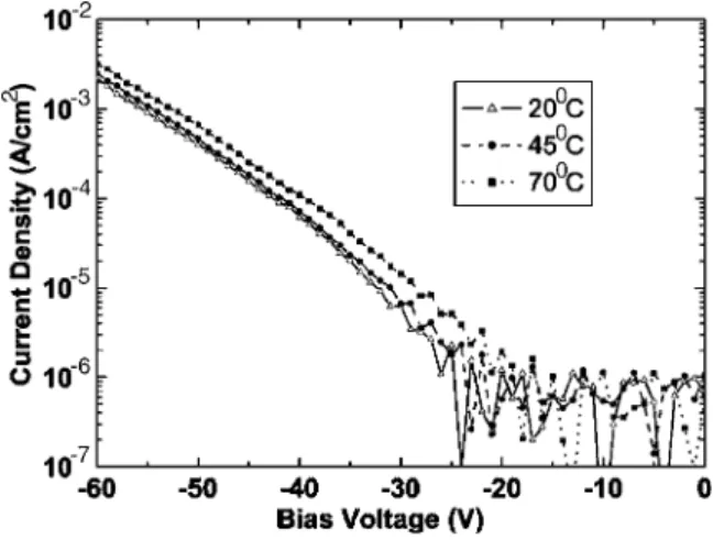
We also measured the dark currents under different tem-peratures. In Fig. 4, the dark current of a photodetector shows a strong dependence on temperature. This result proves that Zener tunneling, which is a temperature insensi-tive process, is not a possible gain mechanism in these de-vices. The gain measurements showed an exponential depen-dence on voltage, in which we infer from this result that the photoconductive gain is not a possible gain mechanism in our devices. We know that the photoconductive gain in-creases linearly with voltage.19,22 Therefore, we conclude that the gain in these devices result from the avalanche mul-tiplication of the photogenerated carriers in the active region of the devices.
In summary, we present the MOCVD growth, fabrica-tion, and characterization of AlGaN-based solar-blind APDs. The avalanche gain at 68 V was in excess of 1560 with no Geiger mode breakdown. The electric field was on the order of 1.88 MV/ cm. The gain in the active region of the devices is attributed to the avalanche multiplication of the photoge-nerated carriers. This work demonstrates the high potential of AlGaN APDs for replacement of the PMTs for high sen-sitive solar-blind photodetector applications.
This work is supported by the European Union under the
projects EU-NoE-METAMORPHOSE,
EU-NoE-PHOREMOST, and TUBITAK under Projects Nos.
104E090, 105E066, 105A005, and 106A017. One of the au-thors 共E.O.兲 also acknowledges partial support from the Turkish Academy of Sciences.
1E. Ozbay, N. Biyikli, I. Kimukin, T. Tut, T. Kartaloglu, and O. Aytur,
IEEE J. Sel. Top. Quantum Electron. 10, 742共2004兲.
2C. J. Collins, U. Chowdhury, M. M. Wong, B. Yang, A. L. Beck, and R. D.
Dupuis, Electron. Lett. 38, 824共2002兲.
3N. Biyikli, T. Kartaloglu, O. Aytur, I. Kimukin, and E. Ozbay, Appl. Phys.
Lett. 79, 2838共2001兲.
4N. Biyikli, I. Kimukin, T. Tut, O. Aytur, and E. Ozbay, Appl. Phys. Lett. 81, 3272共2002兲.
5S. Butun, M. Gokkavas, HongBo Yu, and E. Ozbay, Appl. Phys. Lett. 89,
073503共2006兲.
6J. C. Campbell, S. Demiguel, F. Ma, A. Beck, X. Guo, S. Wang, X. Zheng,
X. Li, J. D. Beck, M. A. Kinch, A. Huntington, L. A. Coldren, J. Decobert, and N. Tscherptner, IEEE J. Quantum Electron. 10, 777共2004兲.
7T. Tut, S. Butun, B. Butun, M. Gokkavas, H. B. Yu, and E. Ozbay,
Appl. Phys. Lett. 87, 223502共2005兲.
8N. Biyikli, I. Kimukin, T. Kartaloglu, O. Aytur, and Ekmel Ozbay,
Phys. Status Solidi C 7, 2314共2003兲.
9Y. Wang, K. Brennan, and P. Ruden, IEEE J. Quantum Electron. 27, 232
共1991兲.
10P. Ruden and S. Krishnankutty, IEEE Trans. Electron Devices 46, 2348
共1999兲.
11C. Sevik and C. Bulutay, Appl. Phys. Lett. 83, 1382共2003兲.
12K. A. McIntosh, R. J. Molnar, L. J. Mahoney, A. Lightfoot, M. W. Geis,
K. M. Molvar, I. Melngailis, R. L. Aggarwal, W. D. Goodhue, S. S. Choi, D. L. Spears, and S. Verghese, Appl. Phys. Lett. 75, 3485共1999兲.
13J. C. Carrano, D. J. H. Lambert, C. J. Eiting, C. J. Collins, T. Li, S. Wang,
B. Yang, A. L. Beck, R. D. Dupuis, and J. C. Campbell, Appl. Phys. Lett.
76, 924共2000兲.
14A. Osinsky, M. S. Shur, R. Gaska, and Q. Chen, Electron. Lett. 34, 691
共1998兲.
15S. Verghese, K. A. McIntosh, R. J. Molnar, L. J. Mahoney, R. L.
Aggarwal, M. W. Geis, K. M. Molvar, E. K. Duerr, and I. Melngailis, IEEE Electron Device Lett. 48, 502共2001兲.
16K. A. McIntosh, R. J. Molnar, L. J. Mahoney, K. M. Molvar, N. Efremov,
and S. Verghese, Appl. Phys. Lett. 76, 3938共2000兲.
17B. Yang, T. Li, K. Heng, C. Collins, S. Wang, J. C. Carrano, R. D. Dupuis,
J. C. Campbell, M. J. Schurman, and I. T. Ferguson, IEEE J. Quantum Electron. 36, 1389共2000兲.
18J. B. Limb, D. Yoo, J. H. Ryou, W. Lee, S. C. Shen, R. D. Dupuis, M. L.
Reed, C. J. Collins, M. Wraback, D. Hanser, E. Preble, N. M. Williams, and K. Evans, Appl. Phys. Lett. 89, 011112共2006兲.
19R. McClintock, A. Yasan, K. Minder, P. Kung, and M. Razeghi,
Appl. Phys. Lett. 87, 241123共2005兲.
20T. Tut, M. Gokkavas, B. Butun, S. Butun, E. Ulker, and E. Ozbay,
Appl. Phys. Lett. 89, 183524共2006兲.
21T. Tut, N. Biyikli, I. Kimukin, T. Kartaloglu, O. Aytur, S. Unlu, and E.
Ozbay, Solid-State Electron. 49, 117共2005兲.
22S. M. Sze, Physics of Semiconductor Devices, 2nd ed.共Wiley, New York,
1981兲, Chap. 13, p. 744. FIG. 4. Dark current measurement data with varying temperatures.