High sensitivity and multifunctional micro-Hall sensors fabricated using InAlSb/
InAsSb/InAlSb heterostructures
M. Bando, T. Ohashi, M. Dede, R. Akram, A. Oral, S. Y. Park, I. Shibasaki, H. Handa, and A. Sandhu
Citation: Journal of Applied Physics 105, 07E909 (2009); View online: https://doi.org/10.1063/1.3074513
View Table of Contents: http://aip.scitation.org/toc/jap/105/7
Published by the American Institute of Physics
Articles you may be interested in Ultra-sensitive graphene Hall elements
Applied Physics Letters 104, 183106 (2014); 10.1063/1.4875597
Flicker noise and magnetic resolution of graphene hall sensors at low frequency
Applied Physics Letters 103, 112405 (2013); 10.1063/1.4821270
Highly sensitive micro-Hall devices based on heterostructures
Journal of Applied Physics 98, 014506 (2005); 10.1063/1.1954867
Small epitaxial graphene devices for magnetosensing applications
Journal of Applied Physics 111, 07E509 (2012); 10.1063/1.3677769
Ultra-sensitive Hall sensors based on graphene encapsulated in hexagonal boron nitride
Applied Physics Letters 106, 193501 (2015); 10.1063/1.4919897
Characteristics of a sensitive micro-Hall probe fabricated on chemical vapor deposited graphene over the temperature range from liquid-helium to room temperature
High sensitivity and multifunctional micro-Hall sensors fabricated using
InAlSb/InAsSb/InAlSb heterostructures
M. Bando,1T. Ohashi,1M. Dede,2R. Akram,2A. Oral,3S. Y. Park,4,5I. Shibasaki,6 H. Handa,5,7and A. Sandhu4,5,7,a兲
1
Department of Electrical and Electronic Engineering, Tokyo Institute of Technology, 2-12-1 O-okayama, Meguro-ku, Tokyo 152-8550, Japan
2Department of Physics, Bilkent University, 06800 Bilkent, Ankara, Turkey
3Faculty of Engineering and Natural Sciences, Sabanci University, Orhanli-Tuzla, 34956 Istanbul, Turkey 4Quantum Nanoelectronics Research Center, Tokyo Institute of Technology, Tokyo 152-8552, Japan 5Tokyo Tech Global COE Program on Evolving Education and Research Center For Spatio-Temporal
Biological Network, Japan
6Asahikasei Corporation, 2-1 Samejima, Fuji City, 416-8501, Japan
7Integrated Research Institute, Tokyo Institute of Technology, 2-12-1 Ookayama, Meguro-ku, Tokyo,
152-8550, Japan
共Presented 12 November 2008; received 25 September 2008; accepted 9 December 2008; published online 12 March 2009兲
Further diversification of Hall sensor technology requires development of materials with high electron mobility and an ultrathin conducting layer very close to the material’s surface. Here, we describe the magnetoresistive properties of micro-Hall devices fabricated using InAlSb/InAsSb/ InAlSb heterostructures where electrical conduction was confined to a 30 nm-InAsSb two-dimensional electron gas layer. The 300 K electron mobility and sheet carrier concentration were 36 500 cm2V−1s−1 and 2.5⫻1011 cm−2, respectively. The maximum current-related sensitivity was 2 750 V A−1T−1, which was about an order of magnitude greater than AlGaAs/ InGaAs pseudomorphic heterostructures devices. Photolithography was used to fabricate 1 m ⫻1 m Hall probes, which were installed into a scanning Hall probe microscope and used to image the surface of a hard disk. © 2009 American Institute of Physics.关DOI:10.1063/1.3074513兴
I. INTRODUCTION
Hall effect magnetic field sensors are ubiquitous. Appli-cations include monitoring the rotation of mechanical parts in electronic equipment and measurement of electric currents in power cables. Further, micro-Hall sensors have also been used for novel applications including scanning Hall probe microscopy共SHPM兲 of ferromagnetic domains1–3and as bio-sensors for the detection of superparamagnetic particles for biorecognition.4,5
Future room temperature applications of Hall sensor technology require development of materials exhibiting high electron mobility and ultrathin conducting layers close to the material’s surface. For a fixed device size and geometry, the magnetic field sensitivity of Hall sensors scales with the electron mobility and nanometer-scale conduction channels are important for forming submicron devices.6
Here, we describe the magnetoresistive properties of micro-Hall devices fabricated using InAlSb/InAsSb/InAlSb quantum well 共QW兲 heterostructures grown by molecular beam epitaxy.7Electrical conduction was confined to a two-dimensional electron gas共2DEG兲 layer in the 30 nm InAsSb. The room temperature electron mobility and sheet carrier concentration were 36 500 cm2V−1s−1 and 2.5 ⫻1011 cm−2, respectively. The current-related sensitivity of Hall devices was 2 750 V A−1T−1, which is about an order of magnitude greater than AlGaAs/InGaAs pseudomorphic
device structures. We compare the performance of InAlSb/ InAsSb/InAlSb heterostructure Hall sensors with AlGaAs/ InGaAs devices and demonstrate the exceeding potential of the former by using a scanning Hall probe microscope to image localized magnetic fields at the surface of a hard disk.
II. EXPERIMENTS
The InAlSb/InAsSb/InAlSb heterostructures were grown using molecular beam epitaxy on semi-insulating 共100兲 GaAs substrates. An insulating layer of 600 nm InAlSb was first grown on the substrates, followed by the deposition of 30 nm undoped InAsSb active layer, 55 nm InAlSb layer, and 6.5 nm of insulating GaAs as a protection layer.
The fabrication process involved 共1兲 formation of the active “cross” area using a combination of photolithography and wet chemical etching; 共2兲 deposition of AuGe Ohmic contacts by vacuum evaporation as described before;8 and 共3兲 thermal annealing in a nitrogen atmosphere at 600 K for 3 min.
The Hall mobility and sheet carrier concentrations were determined by the van der Pauw method and noise measure-ments carried out using digital sampling oscilloscope and fast Fourier transform 共FFT兲 analyzer.9 Magnetic imaging was carried out by mounting InAlSb/InAsSb/InAlSb micro-Hall probes into a scanning micro-Hall probe microscope system to observe the magnetic domains on the surface of a hard disk.10
a兲Electronic mail: [email protected].
JOURNAL OF APPLIED PHYSICS 105, 07E909共2009兲
III. RESULTS AND DISCUSSIONS
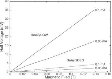
The room temperature electron mobility and the sheet carrier density of a InAlSb/InAsSb/InAlSb heterostructure with a 30 nm InAsSb layer were 36 500 cm2V−1s−1 and 2.5⫻1011 cm−2, respectively. Further, the Hall voltage was extremely linear for bias magnetic fields up to 0.14 T. Figure 1 is a comparison of the variation in the Hall voltage with magnetic field for AlGaAs/InGaAs 2DEG and the anti-monide heterostructures with identical geometry. The results showed excellent linearity.
The absolute sensitivity SA and the supply-current-related sensitivity 共SCRS兲 SI of a cross-shaped Hall sensor can be expressed as follows:
SA⬅ dVH dB共V T −1兲, 共1兲 SI⬅ 1 ID dVH dB = 1 nse 共V A−1T−1兲, 共2兲
where VHis the Hall voltage, B is the applied external mag-netic field, IDis the driving current, and nsis the sheet carrier concentration. From Eq. 共2兲 it can be seen that SCRS de-pends on the sheet carrier concentration. At moderate driving currents the SCRS for InAlSb/InAsSb/InAlSb was as high as 2750 V A−1T−1, whereas AlGaAs/InGaAs with a typical n
s of 2.0⫻1012 cm−2 had 310 V A−1T−1. Figure2 shows the supply-current-related sensitivity as a function of driving current ID. As implied by Eq.共2兲, the driving current versus the SCRS serves as a monitor of carrier fluctuations caused by thermal or electrical activation processes.6 Our results show negligible carrier fluctuations thus, SI was constant at moderate driving currents. The decrease in SCRS at ID ⬎1 mA indicates the excessive driving current causes ther-mal carrier activation.6
The noise spectra of InAlSb/InAsSb/InAlSb Hall sensors were measured using a FFT signal analyzer at sampling rate of 6.25 Hz for a range of drive current. The minimum de-tectable magnetic field using a Hall sensor can be expressed as
Bmin=Vnoise
SIID
. 共3兲
The noise spectra were measured at ID= 10, 50, and 100 A. Table I shows the minimum detectable magnetic field of InAlSb/InAsSb/InAlSb and AlGaAs/InGaAs at the afore-mentioned driving currents and frequencies of 1 and 100 kHz. The results show the magnetic field resolution of InAlSb/InAsSb/InAlSb devices to be about five to ten times better than that of AlGaAs/InGaAs heterostructure Hall sen-sors. The results can be explained by the high SCRS which results from the low sheet carrier concentration of the anti-monide heterostructures as implied from Eq. 共2兲 and low series resistance of InAlSb/InAsSb/InAlSb devices. The se-ries resistance of InAsSb QW and GaAs 2DEG were 1.6 and 3.0 k⍀, respectively. Assuming the Johnson noise Vn =
冑
4kBTR⌬f to be the main noise component in the Hallsensor, where kB, T, R, and⌬f are the Boltzmann’s constant, temperature, series resistance of the device, and the measure-ment bandwidth, respectively; Eq. 共3兲 yields the minimum detectable field of InAlSb/InAsSb/InAlSb at ID= 100 A to be 0.51 mG/
冑
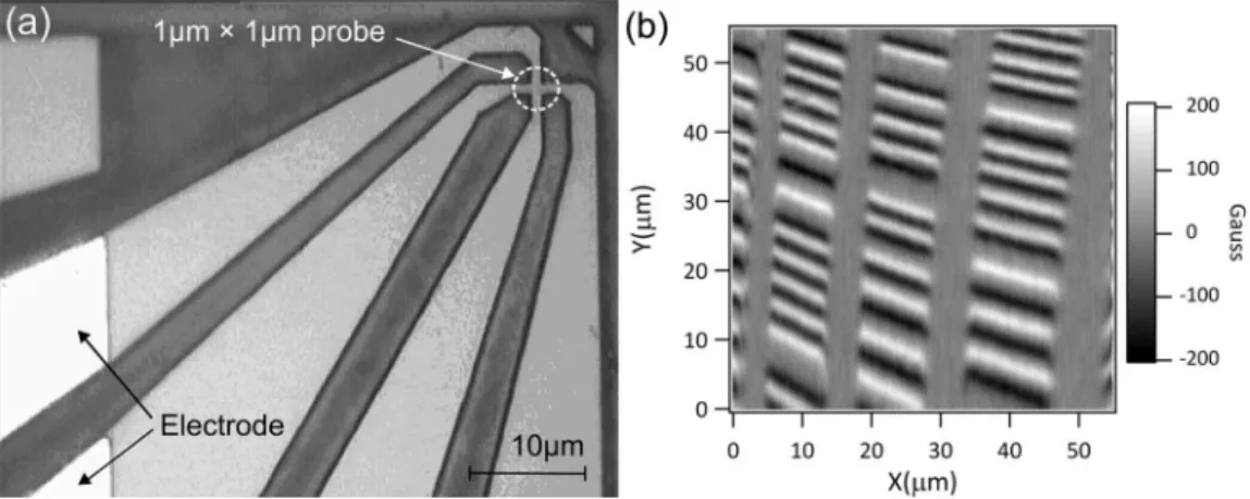
Hz which agrees with the measured magnetic field resolution.The InAlSb/InAsSb/InAlSb heterostructures were used to fabricate micro-Hall probes for use in a scanning Hall probe microscope.10 Figure 3共a兲 is a scanning electron mi-croscope image of a typical Hall probe, where the active cross is 1⫻1 m2.
Figure3共b兲 shows an SHPM image of the surface of a hard disk measured with ID= 500 A at room temperature. 0 5 10 15 20 25 30 35 40 0 0.02 0.04 0.06 0.08 0.1 0.12 0.14 0.16 Hall Voltage (mV) Magnetic Filed (T) 0.05 mA 0.1 mA 0.05 mA 0.1 mA InAsSb QW GaAs 2DEG
FIG. 1. 300 K Hall voltage of InAlSb/InAsSb/InAlSb and AlGaAs/InGaAs as a function of the applied magnetic field for several driving currents.
500 1000 1500 2000 2500 3000 0.001 0.01 0.1 1 10 SC R S( V /AT )
Driving Current (mA)
FIG. 2. The SCRS as a function of the driving current for InAlSb/InAsSb/ InAlsb at 300 K.
TABLE I. The magnetic field resolutions of InAlSb/InAsSb/InAlSb and AlGaAs/InGaAs at 1 and 100 kHz.
Magnetic field resolution共mG/冑Hz兲
1 kHz 100 kHz ID 共A兲 InAsSb QW GaAs 2DEG InAsSb QW GaAs 2DEG 10 6.5 56 0.54 2.5 50 1.1 7.91 0.072 0.49 100 0.58 4.83 0.052 0.30
The image is 50⫻50 m2 and the gray scale shows the magnetic field variations of ⫾200 G. The hard disk had striped magnetic domains in which the moment is oriented perpendicular to the surface and each magnetic bit was clearly resolved and detected.
IV. CONCLUSIONS
High mobility InAlSb/InAsSb/InAlSb heterostructures with 2DEG only about 60 nm from the material’s surface were used to fabricate micro-Hall sensors. The room tem-perature figures of merit of the devices were better than GaAs-based Hall sensors with a current sensitivity of 2750 V A−1T−1, which was an order magnitude greater than conventional GaAs 2DEG Hall sensors. The InAlSb/InAsSb/ InAlSb were used to fabricate micro-Hall probes and the surface of a hard disk was imaged by SHPM. Future experi-ments include fabrication of sub-100 nm Hall probes for SHPM imaging and fabrication of Hall biosensors for detec-tion of superparamagnetic particles in biorecognidetec-tion plat-forms.
ACKNOWLEDGMENTS
This research was partly supported by the Japanese Min-istry of Education, Culture, Sports, Science and Technology 共MEXT兲.
1A. Oral, S. J. Bending, and M. Henini,Appl. Phys. Lett.69, 1324共1996兲.
2Z. Primadani, H. Osawa, and A. Sandhu, J. Appl. Phys. 101, 09K105
共2007兲.
3T. Schweinböck, D. Weiss, M. Lipinski, and K. Eberl,J. Appl. Phys.87,
6496共2000兲.
4G. Mihajlović, P. Xiong, S. V. Monár, K. Ohtani, H. Ohno, M. Field, and
G. J. Sullivan,Appl. Phys. Lett.87, 112502共2005兲.
5Y. Kumagai, M. Abe, S. Sakamoto, H. Handa, and A. Sandhu,J. Appl.
Phys.103, 07A309共2008兲.
6V. P. Kunets, W. T. Black, Yu. I. Mazur, D. Guzun, G. J. Salamo, N. Goel,
T. D. Mishima, D. A. Deen, S. Q. Murphy, and M. B. Santos,J. Appl.
Phys.98, 014506共2005兲.
7A. Okamoto, H. Geka, I. Shibasaki, and K. Yoshida,J. Cryst. Growth278,
604共2005兲.
8A. Sandhu, A. Okamoto, I. Shibasaki, and A. Oral, Microelectron. Eng.
73–74, 524共2004兲.
9A. Oral, K. Kaval, M. Dede, H. Masuda, A. Okamoto, I. Shibasaki, and A.
Sandhu,IEEE Trans. Magn.38, 2438共2002兲.
10NanoMagnetics Instruments Ltd, http://www.nanomagnetics-inst.com.
FIG. 3.共a兲 A typical InAlSb/InAsSb/InAlSb Hall probe with an active area of about 1⫻1 m2Hall used for magnetic imaging with a scanning Hall probe
microscope.共b兲 SHPM 50⫻50 m2magnetic image of a hard disk measured using 1⫻1 m2InAlSb/InAsSb/InAlSb Hall probe. The magnetic field scale
from black to white is⫾200 G.