Passivation of type II InAs/GaSb superlattice photodetectors with
atomic layer deposited Al
2O
3Omer Salihoglu
a,*, Abdullah Muti
a, Kutlu Kutluer
b, Tunay Tansel
b, Rasit Turan
b, Coskun Kocabas
aand Atilla Aydinli
aa
Department of Physics, Bilkent University, 06800 Ankara, Turkey
b
Department of Physics, Middle East Technical University, 06531 Ankara, Turkey
ABSTRACT
We have achieved significant improvement in the electrical performance of the InAs/GaSb midwave infrared photodetector (MWIR) by using atomic layer deposited (ALD) aluminium oxide (Al2O3) as a passivation layer. Plasma
free and low operation temperature with uniform coating of ALD technique leads to a conformal and defect free coverage on the side walls. This conformal coverage of rough surfaces also satisfies dangling bonds more efficiently while eliminating metal oxides in a self cleaning process of the Al2O3 layer. Al2O3 passivated and unpassivated diodes
were compared for their electrical and optical performances. For passivated diodes the dark current density was improved by an order of magnitude at 77 K. The zero bias responsivity and detectivity was 1.33 A/W and 1.9 x 10¹³
Jones, respectively at 4 µm and 77 K. Quantum efficiency (QE) was determined as %41 for these detectors.
Keywords: Superlattice, Photodetector, InAs/GaSb, Al2O3, ALD, Passivation
1. INTRODUCTION
Type-II super lattice (T2SL) InAs/GaSb photodetectors have recently received great interest in the development of midwave and long wave infrared detectors due to advantages like band gap engineering [1], suppression of Auger recombination [2], and interband tunneling [3]. Type-II super lattice technology is a very promising alternative to MCT and QWIP in focal plane array (FPA) applications where, low dark current below 77 K is required. As the confinement of current requires the fabrication of a mesa structure, one of the challenges of T2SL system is the large number of surface states generated due to the abrupt termination of the crystal structure on the mesa side walls. Dangling bonds, inversion layer and interfacial traps are possible sources of surface leakage currents. Small pixel size photodetectors suffer from surface leakage more than large pixel photodetectors due to high perimeter to area ratio. Especially for the FPA applications and long wavelength operations, passivation becomes a vital issue. In order to overcome surface leakage currents of small sized photodetectors, various passivation methods such sulfide [4, 5], silicondioxide layers [6], polymeric layer [7] and even overgrowth with wide bandgap materials [8] were proposed. Passivation is expected to suppress oxidation of the side walls and saturate dangling bonds to prevent surface states. In sulfur passivation, oxygen is replaced with sulfur at the mesa side walls saturating dangling bonds [5, 9]. It is a very effective passivation method and relatively easy to apply nonetheless the effect of passivation is not permanent. Also some reports claim that sulfur passivation damages the surface of the photodetector [9]. Despite the fact that silicondioxide has been shown to be an effective technique, the high temperature or high RF power requirements carries potential for damage. Relatively high growth temperatures (400 0C), may damage SL surfaces and high density energetic ions in a plasma can cause damage
on SL surfaces.
In this work, we report on the study of Al2O3 as a passivation layer for InAs/GaSb SL photodetectors. We
choose to use atomic layer deposition (ALD) to apply the Al2O3. With sequential gas phase reactions, ALD is a self
limiting process. The growth of Al2O3 with ALD uses two gasses that are introduced to the chamber one at a time and
which react with the gas on the surface adsorbed during the previous sequence. ALD deposited Al2O3 has many
advantages as a passivation layer such as the control of thickness at the molecular level since in the ALD process, thickness depends on the number of reaction cycles. This leads to precise thickness control as well as perfect conformal coverage even at sharp edges, large area thickness uniformity, very low process temperatures and plasma free operation. Furthermore Al2O3 is a very good dielectric over a very large frequency range. Due to very thin multiple InAs/GaSb
pairs inT2SL photodetectors, mesa etching leads to uneven etching of the side walls where conformal coverage at the atomic level is very beneficial. Oxidation of the freshly etched surfaces is typically very rapid and a thin layer of oxides forms almost immediately prior to passivation. A successful passivation technique must be eliminate the native oxides formed between mesa etching and passivation steps. Thus a self cleaning procedure eliminating the already formed thin oxide layer would be most welcome. Studies on the surface and interface chemistry of III-V surfaces passivated with atomic layer deposited Al2O3 has shown that it is possible to reduce the native oxides during deposition. This is due to
the fact that formation of Al2O3 is energetically preferred due to lower Gibbs free energy of Al2O3 (-377.9 kcal/mol)
[10]. The Gibbs free energies of Ga2O, Ga2O3, In2O3, As2O3, As2O5 and Sb2O3 which are -75.3 kcal/mol, -238.6
kcal/mol, -198.6 kcal/mol, -137.7 kcal/mol, -187.0 kcal/mol and -151.5 kcal/mol, respectively [11, 12] which are all higher than Al2O3. X-ray photoelectron spectroscopy (XPS) by Hinkle et al. has shown that deposition of Al2O3 on
etched GaAs strongly reduces Ga and As oxides [13]. ALD Al2O3 on InAs has also shown strong reduction of In and As
oxides [14]. MOS capacitors fabricated on GaSb has demonstrated strong suppression of Sb2O3 due to Al2O3 deposition
[15]. These properties of ALD grown Al2O3 makes it a perfect candidate for passivation of InAs/GaSb super lattice FPA
photodetectors. No use of Al2O3 as a passivation layer has been made so far for InAs/GaSb super lattice system.
2. EXPERIMENTAL
The SL structure was designed for MWIR operation and was grown commercially (IQE Inc. USA) with molecular beam epitaxy on a GaSb substrate. The photodetector is designed as p-i-n photodetector with design cutoff wavelength of 5 µm. Figure 1a. shows periodic structure of the p-i-n design superlattice crystal with corresponding thicknesses and doping concentrations.
It starts with 100 nm thick GaSb buffer layer and 20 nm Al(x)GaAs(y)Sb as an insulator and etch stop layer, followed by
1000 nm GaSb:Be (p=1.0x1017 cm-3) p contact layer. Pin part of the design consist of 90 periods 8 monolayers InAs/8
MLs GaSb:Be (p=1.5x1017 cm-3), 60 periods 8 monolayers InAs / 8 MLs GaSb, 60 periods 8 monolayers InAs:Te (n:
5x1017 cm-3)/8 MLs GaSb:Be and structure terminated by 20 nm InAs:Te (n: 5x1017 cm-3) cap layer to assure good ohmic
contact. Appropriate shutter sequences were applied to compensate the tensile strain caused by lattice mismatch between InAs and GaSb layers.
Single pixel photodetectors were fabricated with mesa sizes between 200×200 and 600×600 µm by standard lithography and wet etch solution. For wet chemical etching, orthophosphoric acid (85%), citric acid (100.0%), hydrogen peroxide (30%) solutions and deionized water are used. Mesa-isolated photodiodes are defined at room temperature, using the chemical solution based on H3PO4/ C6H8O7/H2O2/H2O with 200 nm per minute etch rate. The etch process has
been stopped when etch depth reached the bottom contact layer. The etch depth was about 1.5 µm. Figure 1b shows device structure of the p-i-n photodiode. 200 cycles Al2O3 passivation layer deposition carried out in atomic layer
deposition system (Cambridge Nanotech Savannah 100) with 150 Co as the substrate holder temperature. Growth of
Al2O3 has been done by delivering 0.015 s water vapor (H2O) and 0.015 s trimethylaluminum (TMA) pulses into the
chamber in a sequential manner under constant 20 sccm N2 gas flow. A wait time of 20 s was added after each pulse to
ensure surface ractions to take place. Both trimethylaluminum and water were unheated. The thickness of the film grown in this manner was determined as 20 nm by subsequent etching and measurement of the Al2O3 film. For
comparison purpose, same etch procedure was used to fabricate photodetectors with SiOx passivation layer. SiOx
passivation layer deposition carried out in plasma enhanced chemical vapor deposition (PECVD) system at 160 0C and
the process was carried out under the pressure of 0.5 Torr and RF power of 9 W. Flow rates were 180 sccm for SiH4 (%2
in N2) and 225 sccm for N2O. Final thickness of the SiO2 film was about 300 nm. Exact same procedures were applied to
another sample without passivation layer to act as a reference detector. 5 nm Titanium (Ti) and 200 nm Gold (Au) on the bottom and top contact layers of the detectors were evaporated for ohmic contacts.
3. RESULTS AND DISCUSSIONS
The effect of Al2O3 passivation was studied on samples which were mounted on a liquid nitrogen cooled cold
finger. Dark current measurements were performed at 77 K by using a HP4142OA source-measure unit. Figure 2a shows the measured dark current density vs applied bias voltage characteristics of the unpassivated, SiOx and Al2O3 passivated
400x400 µm single pixel test diodes at 77 K. Al2O3 passivated detectors show reduction in dark current density by two
orders of magnitude compared with unpassivated detectors and an order of magnitude reduction when compared with SiOx passivated photodetectors. At -0.1 V bias voltage, dark current densities are measured as 6.5 x 10⁻⁵ A/cm2, 4.1 x 10 -6 A/cm2 and 6.6 x 10⁻⁷ A/cm2 for the unpassivated, SiO
x passivated and Al2O3 passivated diodes, respectively. These
measurements yielded R0A product values of 1.4 x 10³ Ω·cm2, 4.0 x 10⁴ Ω·cm2 and 3.7 x 10⁵ Ω·cm2 for the unpassivated,
SiOx passivated and Al2O3 passivated samples, respectively. SiOx passivation is an industry standard for FPA fabrication.
Our electrical measurements showed that Al2O3 is a better alternative for SiOx passivation. The significant reduction in
dark current and increase in dynamic resistance due to ALD deposited Al2O3 passivation is very encouraging for use in
FPA applications [9, 16, 17]. The inverse of the dynamic resistance area product at zero bias as a function of the perimeter to area ratio at 77K for passivated and unpassivated detectors are shown in Fig. 2b. The surface part of the resistance-area product can be calculated from the slope of the graph [9]. Calculated surface resistivity (rsurface) values at
zero bias are 6.9 x 10⁴ Ω·cm, 2.9 x 10⁵ Ω·cm and 1.3 x 10⁷ Ω·cm for unpassivated, SiO
x passivated and Al2O3 passivated
photodiodes, respectively. The results reveal that Al2O3 passivated diodes show improved surface resistance (rsurface) of a
factor of 200 and 50 when it is compared with unpassivated and SiOx passivated diodes, respectively at 77K. This clearly
shows that Al2O3 passivation suppresses the surface related current more efficiently than SiO2 passivation.
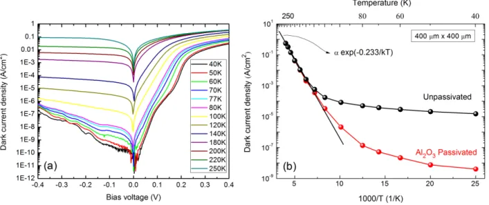
To understand nature of the dark current, temperature dependent measurements of the dark current has been done. Figure 3a shows dark current density vs applied bias voltage for temperatures between 40 K and 250 K. For temperatures lower than 60K, dark current becomes too small for our measurement system and leads to noise around zero bias point. This noise is amplified when dynamic resistance is calculated. We, therefore, prefer to use the dark current vs 1000/T graph to analyze surface leakage currents. Relationship between the dark current densities and inverse temperatures at -0.1V bias are shown in Figure 3b. The current voltage (I-V) curve is dominated by diffusion current at high temperatures and generation-recombination current at mid temperatures. For the lower temperatures surface currents become dominant.
Figure 2. (a) Dark current density vs. applied bias of unpassivated, SiOx passivated and Al2O3 passivated single pixel square diodes measured at 77K. (b) Dependence of dynamic resistance-area product at zero bias vs. perimeter to area ratio for unpassivated and passivated devices at 77K. Slope is directly proportional to the surface related leakage current of the diode.
The diodes with Al2O3 passivation show lower dark currents than unpassivated photodetectors at low temperatures. This
indicates that the Al2O3 passivation satisfies surface states and prevents current flow through the surface channel.
Al2O3 passivated photodetectors show Arrhenius type behavior above 100 K, characterizing the dominant bulk diffusion
current. The activation energy has been calculated as 0.233 eV which is close to the band gap of the device. For lower temperatures, current starts to divert from the Arrhenius type of behavior. Generation recombination (G-R) current becomes dominant for mid temperatures. At 40 K, dark current density shows tendency to decrease, indicating that surface leakage starts to become important in this range [18]. For the unpassivated detector, dark current density deviate from the Arrhenius type of behavior at the temperatures lower than 140 K indicating surface related currents start to become dominant at this range.
Figure 3. (a) Dark current density vs. applied bias of Al2O3 passivated 400 µm single pixel square diodes measured at different temperatures. (b) Temperature dependent dark current measurements of Al2O3 passivated and unpassivated photodetectors at -0.1 V bias.
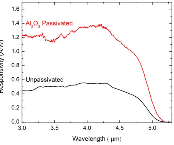
Fourier transform infrared spectroscopy (Bruker Equinox 55) and a liquid nitrogen cooled cold finger system was used to measure spectral response of the photodetectors. Figure 4 shows responsivity vs wavelength graphs of the unpassivated and Al2O3 passivated photodetectors measured under single pass and front side illumination conditions. For
both Al2O3 passivated and unpassivated photodetectors, the cut-off wavelength is determined to be 5.1 µm.
Figure 4. Spectral responsivity of the unpassivated and Al2O3 passivated photodetectors at 77K. The cut-off wavelength of the Al2O3 passivated and unpassivated photodetectors is ~5.1 µm.
A calibrated blackbody source at 800 0C (Newport, Oriel 67000), lock-in amplifier (SRS, SR830 DSP) and
mechanical chopper (SRS, SR540) system was used to measure the responsivity of the photodetectors at 77 K . The detectors were illuminated with a 300 K background with a 2π field-of-view. A 3-5 µm blackbody filter has been use to eliminate unwanted illumination. Quantum efficiency (QE) and Johnson-noise limited detectivity (D*) versus applied bias voltage for Al2O3 passivated photodetector is shown in Figure 3. The zero bias responsivity was equal to 1.33 A/W
at 4 µm and 77K for Al2O3 passivated photodetectors. The peak D*, was equal to 1.9 x 10¹³ Jones for the Al2O3
passivated single pixel photodetector at 4 µm and 77 K. Under single pass front illumination conditions quantum efficiency (QE) of the passivated photodetector was determined as % 41. A comparison of our results with recent data [9, 16-20], shows that ALD grown Al2O3 passivated T2SL photodetectors are very promising.
Figure 5. Quantum efficiency and detectivity of Al2O3 passivated, 400x400 µm single pixel test detectors at 77K and 4 µm. The zero bias QE and the peak value of detectivity, D* of Al2O3 passivated photodetector was equal to %41 and 1.9 x 10¹³ Jones, respectively.
Oxide layers of few nanometers thick native oxide layers form very quickly on freshly etched surface of the superlattice since they are very reactive [21]. Oxygen reacts with surface metals to form oxides like; Sb2O3, Ga2O3,
In2O3 and As2O3. Conductive surface channel can form and cause large surface dark current due to these native oxides.
Due to favorable Gibbs free energies, Al2O3 formation is energetically preferred to native oxide of InAs and GaSb.
Alternatively, As atoms that form As2O3 or In atoms in an In2O3 molecule are replaced by Al+3 atoms in the TMA
molecule [22]. Similar reaction pathways with oxides of other metal atoms are also possible. These are so called interfacial self cleaning reactions of surface oxides [10].
4. CONCLUSION
In conclusion, suppression of dark current and increase in optical response of the InAs/GaSb superlattice photodetectors with cutoff wavelength at 5.1 µm (MWIR) was demonstrated. ALD deposited Al2O3 passivation layer
was used on InAs/GaSb p-i-n design superlattice photodetectors. Conformal coating of atomic layer deposition creates perfect protective layer against environmental effects especially against oxidation. This conformal coverage of rough surfaces also satisfies dangling bonds more efficiently while eliminating metal oxides in a self cleaning process. Single pixel Al2O3 passivated detectors show two orders of magnitude reduction on dark current density compared with
unpassivated detectors and an order of magnitude reduction compared with SiOx passivated photodetectors. These
measurements yielded R0A product values of 1.4 x 10³ Ω·cm2, 4.0 x 10⁴ Ω·cm2 and 3.7 x 10⁵ Ω·cm2 for the unpassivated,
vs. perimeter to area ratio measurements revealed that Al2O3 passivated diodes improve surface resistance (rsurface) of a
factor of 200 and 50 when it is compared with unpassivated and SiOx passivated diodes, respectively at 77K.
Responsivity and detectivity (D*) are determined as 1.33 A/W and 1.9 x 10¹³ Jones, respectively for the Al
2O3 passivated
photodetector at 4 µm and 77K at zero bias. Quantum efficiency (QE) of the passivated photodetector has been determined as % 41 for single pass front illumination condition. Dark current measurements as a function of temperature revealed that passivated devices show Arrhenius type of behavior at higher temperatures. This is an indication that dominant current is bulk diffusion current. The calculated activation energy was found to be close to the design band gap as 0.233 eV. ALD coating of p-i-n InAs/GaSb superlattice photodetectors with Al2O3 is a efficient passivation
technique.
REFERENCES
[1] Wei Y. and Razeghi M., Phys. Rev. B 69, 085316 (2004).
[2] Grein C. H., Young P. M., and Ehrenreich H., Appl. Phys. Lett. 61, 2905 (1992). [3] Smith D. L. and Mailhiot C., J. Appl. Phys. 62, 2545 (1987).
[4] Plis E., Rodriguea J. B., Lee S. J., and Krishna S., Electron Lett. 42, 1248 (2006). [5] Bessolov V. N. and Lebedev M. V., Semiconductors 32, 1141 (1998).
[6] Gin A., Wei Y., Bae J., Hood A., Nah J., and Razeghi M., Thin Solid Films 447, 489 (2004).
[7] Hood A., Delaunay P. Y., Hoffman D., Razeghi M., and Nathan V., Appl. Phys. Lett. 90, 233513 (2007). [8] Rehm R., Walter M., Fuchs F., Schmitz J., and Fleissner J., Appl. Phys. Lett. 86, 173501 (2005).
[9] Kim H. S., Plis E., Khoshakhlagh A., Mayers S., Gautam N., Sharma Y. D., Dawson L. R., Krishna S., Lee S. J., and Noh S. K., Appl. Phys. Lett. 96, 033502 (2010).
[10] Pulver D., Wilmsen C. Niles W., D., and Kee R., J. Vac. Sci. Technol. B 19, 207 (2001). [11] Hollinger G., Kabbani R. S., and Gendry M., Phys. Rev. B 49, 11159 (1994).
[12] Bard A., Parsons J., R., and Jordan J., "Standard Potentials in Aqueous Solutions", Marcel Dekker Inc., New York, (1985).
[13] Hinkle C.L., Sonnet A. M., E. Vogel M., McDonnel S., Hughes G. J., Milojevic M., Lee B., Aguirre-Tostado F. S., Choi K. J., Kim H. C., Kim J., and Wallace R. M., Appl. Phys. Lett. 92, 071901 (2008).
[14] Timm R., Fian A., Hjort M., Thelander C., Lind E., Andersen J. N., Wernersson L. E., and Mikkelsen A., Appl. Phys. Lett. 97, 132904 (2010).
[15] Ali A., Medan H. S., Kirk A. P., Zhao D. A., Mourey D. A., Hudait M. K., Wallace R. M., Jackson T. N., Bennett B. R., Boos J. B., and Datta S., Appl. Phys. Lett. 97, 143502 (2010).
[16] Herrera M., Chi M., Bonds M., N. Browning D., Woolman J. N., Kvaas R. E., Harris S. F., Rhiger D. R., and Hill C. J., Appl. Phys. Lett. 93, 093106 (2008).
[17] Kim H. S., Plis E., Rodriguez J. B., Bishop G. D., Sharma Y. D., Dawson L. R., Krishna S., Bundas J., Cook R., Burrows D., Dennis R., Patnaude K., Reisinger A., and Sundaram M., Appl. Phys. Lett. 92, 183502 (2008).
[18] Nguyen B. M., Hoffman D., Huang E. K., Bogdanov S., Delaunay P. Y., Razeghi M., and Tidrow Z., Appl. Phys. Lett. 94, 223506 (2009).
[19] Kwei-wei E., Hoffman D., Nguyen B.M., Delaunay P.Y., and Razeghi M., Appl. Phys. Lett. 94, 053506 (2009). [20] Helm R., Walter M., Schmitz J., Rutz F., Fleibner J., Scheibner R., and Ziegler J., Infrared Phys. Technol. 52, 344
(2009).
[21] Cervera C., Rodriguez J. B., Chaghi R., Aït-Kaci H., and Christol P., J. Appl. Phys. 106, 024501 (2009).
[22] Chang C. H., Chiou Y. K., Chang Y. C., Lee K. Y., Lin T. D., Wu T. B., Hong M., and Kwo J., Appl. Phys. Lett. 89, 242911 (2006).