Broadband High-Gain 60 GHz Antenna Array
Md. A. Towfiq , A. Khalat and B. A. Cetiner Electrical and Computer Engineering
Utah State University Logan, Utah
¨
O. Ceylan and N. Biyikli
National Nanotechnology Research Center Bilkent University
Turkey
Abstract—The design, fabrication and characterization of a 2x8 patch antenna array operating in the IEEE 802.11ad frequency band (57-66 GHz) is presented. The design is based on two-layer structures, where the radiating patches placed on top substrate are fed by conductor backed coplanar waveguide (CPW)-fed loop slots, which are placed on the bottom substrate. The top layer is formed by using a low-cost pyrex (εr = 4.9, tanδ = 0.01)
substrate of 500µm thickness. The pyrex is then etched away to a thickness of 100µm, where 400µm of air volume is formed underneath. This approach does not only benefit from the low-cost feature of pyrex but also exploits the low-loss nature of air. The thin layer of pyrex is solely used for mechanical support for the radiating patches while the air provides good RF-environment for the array. The bottom substrate housing the CPW feed network is an RF-compatible and microfabrication friendly quartz (εr = 3.9, tanδ = 0.0002) of 525µm thickness.
The simulations indicate a good maximum realized gain of 19.3 dBi of which variation over ∼ 17% bandwidth is relatively constant changing from 17 - 19.3 dBi.
I. INTRODUCTION
Availability of unlicensed broad frequency band and possi-bility of high speed communication in short range have been attracting great interest for wireless communication systems operating at around 60 GHz commonly known as mm-wave or WiGig band [1]. However, the propagation losses associated with this band are severe, thus limiting the wireless commu-nication coverage to short distances. Therefore, antennas with high gain and broad bandwidth (BW) are needed. The losses associated with conductors, dielectrics and surface waves make designing an antenna with a high gain over a broad bandwidth in the 60 GHz range challenging. Recently, substrates such as SU-8 (εr = 3.1, tanδ = 0.021) which provides some
advan-tages in terms of microfabrication have been used. Although, SU-8 does not have good material properties (very high RF losses) for RF/antenna applications, it can be easily processed to form air cavities within, thereby taking advantage of good material properties of air. A microfabricated SU-8-based patch antenna structure exploiting air cavities was recently reported to achieve 57-66 GHz bandwidth and a maximum realized gain of 7dBi [2]. Also microfabrication techniques in creating closely spaced holes underneath a patch antenna on high dielectric substrate were used to synthesize a low dielectric environment [3].
This work attempts to develop a low-cost high performance (broad impedance BW with high realized gain) antenna array working at 60 GHz. To this end, two-layer antenna structure using the combination of RF-compatible quartz substrate and
low-cost pyrex substrate is adopted. The design strategy is to combine the advantages of multiple approaches of previous works [2]–[5]. The design makes use of CPW loop feeding mechanism on quartz substrate to provide broad BW. It uses low cost pyrex material where air cavities are easily formed by a single process step, which does not only reduce cost but also take advantage of good RF properties of air. It is worth noting that this approach is much simpler and lower cost in terms of microfabrication as compared to forming air cavities in SU-8, which requires multiple process steps [2].
Considering the link-budget requirement at 60 GHz gigabit link [6], a maximum antenna gain of at least 15 dBi is needed. Therefore, it becomes proper to use at least 16 elements array. In this work, 2x8 patch antenna array is presented. The inter element distance of the array is optimized providing low mutual coupling and air bridges used in the feed network helps reduce RF losses by enabling continuous electric field across the T-junctions used. This array achieves 19.3 dBi maximum realized gain and ∼ 17% impedance BW (55-65 GHz) over which the gain remains relatively flat changing from 17 - 19.3 dBi.
II. ANTENNAARRAYDESIGN
The antenna structure as depicted in Fig. 1 consists of two layers. The bottom layer uses quartz substrate which has good RF properties and is compatible with microfabrication processes.The feed metallization consisting of 50Ω conductor backed (CB) CPW and the CPW-loop is formed on this layer. A pyrex substrate with a thickness of 500µm was chemically etched to a thickness of 100µm, which is used as support layer for the radiating patch elements. This thin pyrex layer is aligned and placed on top of the bottom layer. The volume of the air layer with a thickness of 400µm formed under pyrex provides an environment with low dielectric constant along with low loss, which improves the impedance bandwidth and gain. The main role of thin pyrex layer is to provide mechani-cal support for radiating patches. The CB CPW-fed loop, patch size and element spacing are jointly optimized to get a broad BW and maximum realized gain, where the numerical values are given in Table I and Fig. 1. Corporate feeding network with power dividers has been utilized to excite each array element with equal power and phase. Necessary characteristic impedance transformations using quarter wave transformers have also been performed in the T-junction dividers as shown in Fig. 1.
899
Fig. 1. (a) Schematic of 3-D structure of the antenna array showing critical design parameters, (b) Enlarged A-A’, (c) Enlarged B-B’
TABLE I
DESIGN PARAMETERS(DIMENSIONS ARE INmm,λ0DENOTES WAVELENGTH IN AIR AT60 GHZ).
Px 1.5 Lx 1.24 Le 0.7λ0
Py 1.3 Ly 1.04
III. SIMULATIONRESULTS
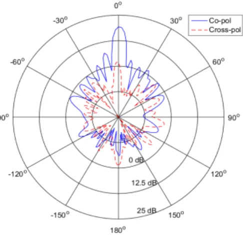
Fig. 2 shows simulated reflection coefficient of the array, where a bandwidth of 10 GHz from 55-65 GHz covering the frequency range of the IEEE 802.11ad is achieved. The simulated radiation pattern of the array in Y-Z plane at 59 GHz is shown in Fig. 3 The realized maximum gain of the array is relatively constant over the entire bandwidth which is in the range of 17-19.3 dB, which is shown in Fig. 4
Fig. 2. Simulated Reflection Coefficient of the antenna array.
IV. CONCLUDINGREMARKS
A CPW-fed patch antenna array compatible with IEEE 802.11ad standard has been designed and characterized. The
Fig. 3. Simulated radiation pattern of the array in Y-Z plane at 59 GHz.
Fig. 4. Simulated realized gain values over 57-65 GHz band.
simulation results indicate relatively constant gain values (17-19.3 dB) over 57-65 GHz band, which makes the designed array a strong candidate for multiGigabit applications. The microfabrication and measurements of the array are already underway.
REFERENCES
[1] C. Hansen, “Wigig: Multi-gigabit wireless communications in the 60 ghz band,” Wireless Communications, IEEE, vol. 18, no. 6, pp. 6–7, December 2011.
[2] H. Mopidevi, H. Hunerli, E. Cagatay, N. Biyikli, M. Imbert, J. Romeu, L. Jofre, and B. Cetiner, “Three-dimensional microfabricated broadband patch antenna for wigig applications,” Antennas and Wireless Propagation Letters, IEEE, vol. 13, pp. 828–831, 2014.
[3] G. Gauthier, A. Courtay, and G. Rebeiz, “Microstrip antennas on syn-thesized low dielectric-constant substrates,” Antennas and Propagation, IEEE Transactions on, vol. 45, no. 8, pp. 1310–1314, Aug 1997. [4] L. Wang, Y.-X. Guo, and W.-X. Sheng, “Wideband high-gain 60-ghz
ltcc l-probe patch antenna array with a soft surface,” Antennas and Propagation, IEEE Transactions on, vol. 61, no. 4, pp. 1802–1809, April 2013.
[5] S. B. Yeap, Z. N. Chen, and X. Qing, “Gain-enhanced 60-ghz ltcc antenna array with open air cavities,” Antennas and Propagation, IEEE Transactions on, vol. 59, no. 9, pp. 3470–3473, Sept 2011.
[6] P. Smulders, H. Yang, and I. Akkermans, “On the design of low-cost 60-ghz radios for multigigabit-per-second transmission over short distances [topics in radio communications],” Communications Magazine, IEEE, vol. 45, no. 12, pp. 44–51, December 2007.