Electronic transport characterization of AlGaN/GaN heterostructures using
quantitative mobility spectrum analysis
S. B. Lisesivdin, A. Yildiz, S. Acar, M. Kasap, S. Ozcelik et al.
Citation: Appl. Phys. Lett. 91, 102113 (2007); doi: 10.1063/1.2778453
View online: http://dx.doi.org/10.1063/1.2778453
View Table of Contents: http://apl.aip.org/resource/1/APPLAB/v91/i10
Published by the American Institute of Physics.
Additional information on Appl. Phys. Lett.
Journal Homepage: http://apl.aip.org/
Journal Information: http://apl.aip.org/about/about_the_journal
Top downloads: http://apl.aip.org/features/most_downloaded
Information for Authors: http://apl.aip.org/authors
Electronic transport characterization of AlGaN / GaN heterostructures
using quantitative mobility spectrum analysis
S. B. Lisesivdin, A. Yildiz, S. Acar,a兲M. Kasap, and S. Ozcelik
Department of Physics, Faculty of Science and Arts, University of Gazi, Teknikokullar, 06500 Ankara, Turkey
E. Ozbay
Nanotechnology Research Center, Department of Physics, and Department of Electrical and Electronics Engineering, Bilkent University, Ankara, Turkey
共Received 4 July 2007; accepted 9 August 2007; published online 6 September 2007兲
Resistivity and Hall effect measurements in nominally undoped Al0.25Ga0.75N / GaN heterostructures
grown on sapphire substrate by metal-organic chemical vapor deposition are carried out as a function of temperature 共20–350 K兲 and magnetic field 共0–1.5 T兲. The measurement results are analyzed using the quantitative mobility spectrum analysis techniques. It is found that there is strong two-dimensional electron gas localization below 100 K, while the thermally activated minority carriers with the activation energies of ⬃58 and ⬃218 meV contribute to the electron transport at high temperatures. © 2007 American Institute of Physics. 关DOI:10.1063/1.2778453兴
High electron mobility transistors 共HEMTs兲 are widely used and accepted as the promising components of the high-speed electronics. Especially, AlxGa1−xN / GaN HEMTs are
the most interesting candidate since their introduction1 and demonstration of high-power operability.2Due to their large band gap energy, large electron drift velocities, high conduc-tion band discontinuity, and high thermal stability, AlxGa1−xN / GaN HEMTs can operate at high power and high
temperature conditions with high two-dimensional electron gas共2DEG兲 sheet carrier density and high mobility values as compared even with GaAs based devices.3,4Even without an intentional doping AlxGa1−xN GaN interface,
AlxGa1−xN / GaN based heterostructures have a 2DEG with
high sheet carrier density values.5,6 The mobility and sheet carrier density of the 2DEG are the most important param-eters in describing the electronic properties of AlxGa1−xN / GaN heterostructures. On the other hand, in
practice, the charge carriers generated by the crystal defects in both bulk GaN and AlxGa1−xN layers, and the 2DEG
car-riers induced by the polarization at the interface can also contribute to the measured data and the electronic properties of AlxGa1−xN / GaN heterostructures. Therefore, even in
nominally undoped AlxGa1−xN / GaN heterostructures, the
mixed conduction can be presented.
However, in the presence of multiple carrier species, the mixed-conduction effects have a strong influence on elec-tronic properties of semiconductor materials, including bulk samples, thin films, quantum wells, and multilayer device structures.7Although single field Hall effect measurements extract only averaged mobility and carrier concentration, single field measurements are used to determine carrier con-centration, band gap, and impurity activation energies and to describe the scattering process involved in the case of single electron, hole conduction, or single band conduction in the semiconductor. In the presence of mixed conduction, there is often a lack of an appreciation of the systematic errors when making these measurements and pitfalls in their interpreta-tion and analysis since, in these measurements, it is assumed
that all carriers have the same drift velocity and the carrier mobility is identical to the minority carrier mobility.8 There-fore, in the mixed conduction case for extracting the correct transport parameters of the individual carriers, resistivity and Hall effect measurements are to be performed as a function of magnetic field. These measurements共variable field兲 allow us to simultaneously characterize densities and mobilities for each of the multiple electron and hole species. Several ap-proaches for analyzing magnetic field dependent resistivity and Hall data from the samples exhibiting mixed conduction have been discussed in several papers.7–10
In this work, the variable field resistivity and Hall effect data were analyzed using the quantitative mobility spectrum analysis共QMSA兲 technique that described and improved in previous studies.11–14Variable field resistivity and Hall coef-ficient measurements in conjunction with the QMSA tech-nique allow extraction of the individual carrier concentra-tions and mobilities in semiconductor materials. Thus, in this study, the individual carries 共2DEG and bulk carriers兲 and their effect on the electron transport are investigated using the QMSA technique in Al0.25Ga0.75N / GaN heterostructures
grown by metal-organic chemical vapor deposition 共MOCVD兲. In a number of papers, the QMSA technique has been used in determining individual carrier densities and mo-bilities in semiconductor materials, including bulk samples, thin films, quantum wells, and multilayer device structures.13–16
The samples investigated in this work were grown on
c-plane共0001兲 sapphire 共Al2O3兲 substrate in a low-pressure MOCVD reactor. The details of the samples are given elsewhere.17
For the resistivity and Hall effect measurements by the van der Pauw method, square shaped 共5⫻5 mm2兲 samples were prepared with four evaporated Ti/ Al/ Ni/ Au Ohmic contacts in the corners. The measurements were made at 24 temperature steps over a temperature range of 20– 350 K us-ing a Lake Shore Hall effect measurement system. At each temperature step, the Hall coefficient and resistivity were measured for both current directions, both magnetic field po-larization, and all possible contact configurations at 31 mag-netic field steps between 0 and 1.5 T. The magmag-netic field
a兲Author to whom correspondence should be addressed; FAX: 903122122279; electronic mail: [email protected]
APPLIED PHYSICS LETTERS 91, 102113共2007兲
0003-6951/2007/91共10兲/102113/3/$23.00 91, 102113-1 © 2007 American Institute of Physics
dependent data are analyzed using the QMSA technique. To confirm the activation energies obtained from the carrier den-sities, which extracted from QMSA, room temperature pho-toluminescence 共RT-PL兲 measurements are also carried out with a Horiba Jobin-Yvon PL system with Kimmon 325 nm He–Cd laser.
To extract individual carriers from the measured field dependent data over studied temperature range are analyzed using the QMSA. First, the longitudinal and transverse con-ductivity tensorsxx共B兲 andxy共B兲 at each temperature step
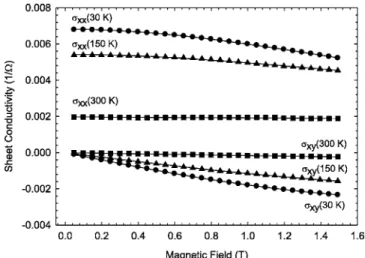
are obtained using the field dependent resistivity and Hall coefficient data as the input parameters in QMSA. For the demonstration, the derived conductivity tensors 共symbols兲 and the fitted results共solid lines兲 from QMSA are given in Fig. 1 for the only three temperatures. A near perfect fit 共solid lines兲 to the data is a good indication of the validity of the QMSA spectrum presented below. It can also be seen from Fig. 1 that both the values of conductivity tensors,
xx共B兲 andxy共B兲, increase with the decreasing temperature.
Second, we have performed the application of the QMSA technique to the measured field-dependent data to obtain the multicarrier mobility spectra at 24 temperature steps in the studied temperature range. For the demonstra-tion, only the QMSA spectra at 30 and 195 K are given in Fig.2. In the studied temperature range, some important dis-tinct features of the mobility spectra have been observed. At
whole temperature range, a main electron peak with a mo-bility close to the measured ones has been obtained from QMSA. At low temperatures共below 150 K兲, only one tron peak is observed, while at high temperatures two elec-tron peaks are presented. In addition to these, at every tem-perature steps, hole peaks with a higher mobility than that of the last electron peak are observed. These peaks nearly over-lap to the last electron peaks at the mobility spectrum, as can be seen from Fig.2.
The mobility of the hole peaks is too high for any known carrier in the AlxGa1−xN / GaN heterostructures. For
AlxGa1−xN / GaN material system, such an unexpected peak
is, therefore, assumed to be unphysical and named as “ghost hole.” Such ghost holes are an artifact of a type that is seen quite frequently in mobility spectrum analyses and even in multicarrier fits.18 Several research groups have reported ghost carriers in their mobility spectrum analysis of different material systems and heterostructures, which emphasizes how pervasive such ghost carriers are.18,19On the other hand, according to the layer structures,17 spontaneous and strain induced polarizations lead to a high positive polarization in the AlGaN, resulting only in 2DEG induced at the AlxGa1−xN / GaN interface. In addition, our structure is
un-doped and it is well known that the crystal defects, such as Ga and N vacancies, in both GaN and AlGaN layers produce shallow donor levels.20 Therefore, in nominally undoped AlxGa1−xN / GaN heterostructures, only the negative charge
carriers 共2DEG and bulk electrons兲 are to be expected. To our knowledge, no satisfying explicit explanation for the ac-tual mechanism of ghost carriers is reported yet. The possible origins of the ghost carriers may include nonideality of mea-surements and the assumptions made in the QMSA.
Figures3共a兲and3共b兲 summarize the QMSA results as a function of temperature for the integrated density and mobil-ity for each electron observed. In Figs. 3共a兲 and 3共b兲, the mobility and carrier density measured at 0.5 T are given with circles. From Fig.3共b兲, it can be clearly understood that the polarizations induced 2DEG carrier species 共n1兲 and
ther-mally activated carriers 共n2 and n3兲 are obtained from
QMSA. The mobility and electron density共triangles兲 for the 2DEG have the same temperature dependence with the mea-sured mobility and carrier density at a single field 共0.5 T兲, and their values are also closer to the measured ones. Both the measured共circles兲 and the 2DEG 共triangles兲 mobility and carrier density are nearly independent of temperature below 100 K, where ionized impurity scattering would be expected to dominate. This behavior is typical of 2DEG structure. Above 100 K, Hall mobilities 共measured and 2DEG兲 crease with increasing temperature with a temperature de-pendence of⬃T−3/2, which is the typical temperature
depen-dence for phonon scattering mobility. The measured and 2DEG carrier densities still tend to be constant, which is a further confirmation of the 2DEG even at high temperature. Therefore, the analyses and measurement suggest that there is strong 2DEG localization below 100 K.
At high temperatures, the existed electrons with high mobility freeze out below 150 K. The existed minority car-riers, which contribute much less to the total conductivity, have been assigned to bulk GaN. The remarkable point to note is that these carriers are quite distinctly evident at a density of only 1010– 1012cm−2, despite the presence of the
much more prominent 2DEG carrier species 共⬃1013cm−2兲. Such sensitivity to low-density electrons has been observed
FIG. 1. Conductivity tensors vs magnetic field at 30, 150, and 300 K. The symbols are the experimental data. The lines represent the fits obtained from QMSA.
FIG. 2. Electron共solid lines兲 and hole 共dashed lines兲 QMSA spectra for Al0.25Ga0.75N / GaN heterostructure at共a兲 30 and 共b兲 195 K.
102113-2 Lisesivdin et al. Appl. Phys. Lett. 91, 102113共2007兲
in the spectra for other semiconductor systems, and QMSA often yields more information about low-density minority carriers with high mobility than any of the other analysis techniques.12 The activation energies of thermally generated minority carriers whose density increases exponentially with temperature are found to be⬃58 and ⬃218 meV for n2and
n3, respectively. We believe that these energies are related
with the shallow defect共impurity and vacancy兲 levels of bulk GaN since the energies of shallow donor levels are reported ranging from 30 to 600 meV in GaN.21
To verify the activation energies obtained from the car-rier densities given in Fig. 3共b兲, RT-PL measurements are also carried out. The results are analyzed using the multiple Gaussian peak analysis technique. RT-PL measurement and analysis results are shown in Fig.4. Band gap energy共Eg兲 of
GaN is obtained as⬃3.41 eV. Three peaks are observed at 92.6, 56.1, and 223.4 meV below the conduction band edge. The energies of two peaks共56.1 and 223.4 meV兲 below EC
are close to the activation energies obtained from the ex-tracted carriers from QMSA. Therefore, these two peaks are attributed as shallow defect levels in GaN. The other peak with 96.2 meV is evaluated as an optical phonon peak since such optical phonon related peaks are usually reported in literature.22,23 It is noted that the transition with 56.1 meV has more strength than the Eg transition due to
overexcite-ment of the 3.81 eV laser, which is larger than the band gap energy.
1M. A. Khan, A. Bhattarai, J. N. Kuznia, and D. T. Olson, Appl. Phys. Lett. 63, 1214共1993兲.
2Y. F. Wu, B. P. Keller, S. Keller, D. Kapolnek, P. Kozodoy, S. P. Denbaars, and U. K. Mishra, IEEE Electron Device Lett. 17, 455共1996兲. 3Y. F. Wu, B. P. Keller, P. Parikh, D. Kapolnek, S. P. Denbaars, and U. K.
Mishra, IEEE Electron Device Lett. 18, 290共1997兲.
4R. Gaska, Q. Chen, J. Yang, A. Osinsky, M. A. Khan, and M. S. Shur, IEEE Electron Device Lett. 18, 492共1997兲.
5O. Ambacher, B. Foutz, J. Smart, J. R. Shealy, N. G. Weimann, K. Chu, M. Murphy, A. J. Sierakowski, W. J. Schaff, L. F. Eastman, R. Dimitrov, A. Mitchell, and M. Stutzman, J. Appl. Phys. 87, 334共2000兲.
6F. Bernardini, F. Fiorentini, and D. Vanderbilt, Phys. Rev. B 56, R10024 共1997兲.
7J. R. Meyer, C. A. Hoffman, F. J. Bartoli, D. J. Arnold, S. Sivananthan, and J. P. Faurie, Semicond. Sci. Technol. 8, 805共1993兲.
8A. Wolkenberg, T. Przeslawski, J. Kaniewski, and K. Reginski, J. Phys. Chem. Solids 64, 7共2003兲.
9B. J. Kelley, B. C. Dodrill, J. R. Lindemuth, G. Du, and J. R. Meyer, Solid State Technol. 12, 130共2000兲.
10J. S. Kim, D. G. Seiler, and W. F. Tseng, J. Appl. Phys. 73, 8324共1993兲. 11J. Antoszewski, D. J. Seymur, L. Farone, J. R. Meyer, and C. A. Hoffman,
J. Electron. Mater. 24, 1255共1995兲.
12J. R. Meyer, C. A. Hoffman, J. Antosewski, and L. Farone, J. Appl. Phys. 81, 709共1997兲.
13B. C. Dodrill, J. R. Lindemuth, B. J. Kelley, G. Du, and J. R. Meyer, Compound Semicond. 7, 58共2001兲.
14J. Antoszewski, L. Faraone, I. Vurgaftman, J. R. Meyer, and C. A. Hoffman, J. Electron. Mater. 33, 673共2004兲.
15M. Kasap and S. Acar, Phys. Status Solidi A 201, 3113共2004兲. 16S. Acar, M. Kasap, B. Y. Isik, S. Ozcelik, N. Tugluoglu, and S. Karadeniz,
Chin. Phys. Lett. 22, 2363共2005兲.
17S. B. Lisesivdin, S. Acar, M. Kasap, S. Ozcelik, S. Gokden, and E. Ozbay, Semicond. Sci. Technol. 22, 543共2007兲.
18N. Biyikli, J. Xie, Y. T. Moon, F. Yun, C. G. Stefanita, S. Bandyopadhyav, H. Morkoç, I. Vurgaftman, and J. R. Meyer, Appl. Phys. Lett. 88, 142106 共2006兲.
19N. N. Berchenko, V. V. Bogoboyashchiy, I. I. Izhin, M. Pociask, E. M. Sheregii, and V. A. Yudenkov, Phys. Status Solidi C 2, 1418共2005兲. 20Z. T. Zhou, L. W. Guo, Z. G. Xing, G. J. Ding, J. Zhang, M. Z. Peng, H.
Q. Jia, H. Chen, and J. M. Zhou, Chin. Phys. Lett. 24, 1641共2007兲. 21V. Bougrov, M. E. Levinshtein, S. L. Rumyantsev, and A. Zubrilov, in
Properties of Advanced Semiconductor Materials GaN, AlN, InN, BN, SiC, SiGe, edited by M. E. Levinshtein, S. L. Rumyantsev, and M. S. Shur 共Wiley, New York, 2001兲, pp. 1–30.
22H. S. Kwack, Y. H. Cho, G. H. Kim, M. R. Park, D. H. Youn, S. B. Bae, K. S. Lee, J. H. Lee, and J. H. Lee, Phys. Status Solidi C 6, 2109共2006兲. 23S. M. Kim, H. S. Kwack, S. W. Hwang, Y. H. Cho, H. I. Cho, J. H. Lee,
and K. L. Wang, Phys. Status Solidi C 6, 2113共2006兲. FIG. 3. 共a兲 Mobility and 共b兲 carrier concentration vs temperature. Circles
represent measured mobility and carrier concentration at 0.5 T. Triangles, stars, and squares represent the mobilities and carrier concentrations ex-tracted from QMSA. Solid lines shown are guides for the eye. Dash-dotted and dashed lines show the proposed trends of thermally activated minority carriers.
FIG. 4. Room temperature PL spectrum. Symbols represent PL measure-ments. Dashed and solid lines represent Gaussian peaks and total Gaussian peaks, respectively.
102113-3 Lisesivdin et al. Appl. Phys. Lett. 91, 102113共2007兲