Contents lists available atScienceDirect
Materials Science in Semiconductor Processing
journal homepage:www.elsevier.com/locate/msspTemperature dependent current-voltage characteristics of Al/TiO
2
/n-Si and
Al/Cu:TiO
2
/n-Si devices
Mehmet Okan Erdal
a, Adem Kocyigit
b, Murat Y
ıldırım
c,* aNecmettin Erbakan University, Meram Vocational School, 42090, Konya, TurkeybIgdir University, Engineering Faculty, Department of Electrical Electronic Engineering, 76000, Igdir, Turkey cSelcuk University, Faculty of Science, Department of Biotechnology, 42130, Konya, Turkey
A R T I C L E I N F O
Keywords:
Cu doped TiO2thinfilms
Al/TiO2/n-Si
Temperature-dependent I–V characteristics Spin coating
A B S T R A C T
We fabricated undoped and Cu doped TiO2thinfilms by spin coating technique and employed the films as
interfacial oxide layer between the Al and n-type Si to investigate the effect of temperature on the Al/TiO2/n-Si
and Al/Cu:TiO2/n-Si devices. For that aim, the I–V measurements were performed in the range of 50 K–400 K by
50 K interval. The devices exhibited good rectifying behavior and thermal response in a wide range temperature. Ideality factor, barrier height and series resistance were calculated from I–V measurements for various tem-peratures by thermionic emission theory, Norde and Cheung methods and discussed in the details. The obtained results revealed that the device parameters are a strong function of the temperature. The interface states (Nss)
were affected by the changing of the temperatures. The Al/TiO2/n-Si and Al/Cu:TiO2/n-Si devices can be
per-formed for wide range temperatures in various technological applications.
1. Introduction
The metal oxides have great interest due to their adjustable beha-viors such as band gap, mobility and conductivity [1–5]. These prop-erties provide good opportunity to employ them for various applica-tions such as solar cells, lasers, photodetectors and photodiodes [6–10]. Among the metal oxide family, TiO2has high dielectric constant, high refractive index and good optical transmittance in the visible range [11,12]. The high dielectric constant in the range of 35–100 makes it a good candidate to be an interlayer for metal-semiconductor devices (MS) both to prevent inter-diffusion and to passivate interface states and dislocations [13]. Thus, the performance of the MS devices can be improved by that way.
The MS devices have gained great attention because of their variety of applications such as inverters, rectifiers and photodiodes [14–16]. The device properties of the MS can be controlled by the interfacial layers via metal oxide or insulators [17–19]. Especially, the TiO2film layers were employed as the interfacial layer in the literature. For ex-ample, Asar et al. [13] investigated voltage and temperature dependent dielectric properties of the (AuZn)/TiO2/p-GaAs MIS device which had TiO2interlayer in the temperature range of 80 K–290 K. Tanrıkulu et al. [20] obtained Au/TiO2/n-4H–SiC MS device with TiO2interlayer and investigated its main electrical and dielectric properties via impedance spectroscopy. They concluded that the TiO2interlayer improved the
performance of the MS device. Bilgili et al. [21] fabricated Ag/TiO2 /n-InP MS device and performed the I–V measurements on the device for wide range temperatures from 120 K to 420 K. Tataroğlu et al. [22] studied NiO-doped TiO2film in between n-Si and Al metal as interfacial layer and concluded that the obtained device exhibited good photo-conductivity and photoresponsivity via changing NiO contents. Yıldırım [23] investigated both optical and electrical properties of the various Cu doped TiO2interfacial layer between the Al and n-Si at room tem-perature. The photoresponse behavior of TiO2is greatly influenced by its crystal structure, particle/grain size, crystallinity, surface area, and porosity. Furthermore, various techniques have been employed to en-hance its properties by doping with metal or non-metal elements in order to narrow its band gap [24]. The modification of Cu dopant can be improved the photoresponse and photocurrent density of TiO2. Moreover, Cu dopants have already shown to play an important role in the effective charge separation in TiO2electron harvesting processes [25]. Blondeau et al. claim that applications for solar energy conversion of doping TiO2with an element taken from metals, their results have shown that this alloying has created an extra level of absorption at energy within the bandgap of TiO2. They have also shown that the concentration of this foreign element was very important to obtain a practical result [26].
In this case, we studied the temperature dependent I–V character-istics of the Cu doped TiO2interfacial layer. It is therefore, we studied
https://doi.org/10.1016/j.mssp.2019.104620
Received 11 April 2019; Received in revised form 4 June 2019; Accepted 13 July 2019
*
Corresponding author.
E-mail address:[email protected](M. Yıldırım).
Available online 17 July 2019
1369-8001/ © 2019 Elsevier Ltd. All rights reserved.
mixed solution and stirred again 5 h. This mixture was employed to synthesize Cu doped TiO2thinfilm.
The n-type Si wafer was used as a substrate and semiconductor. The wafer had (100) preferred crystalline orientation and 7.5 × 1016cm−3 carrier concentration. The n-type Si wafer was cut to 2 cm2pieces, and then the pieces were cleaned by acetone and isopropanol alcohol in an ultrasonic bath and dried in nitrogen. The pieces were dumped into HF:H2O (1:1) mixed solution to remove the impurities and native SiO2 oxide layers from the surfaces. To obtain ohmic contact on the back surface of the Si pieces, highly pure Al (99.999%) was evaporated at 150 nm thicknesses at 5 × 10⁻⁶torr pressure. The Si wafer pieces were annealed in nitrogen medium at 500 °C for 3 min after Al evaporation. The obtained solutions for undoped and Cu doped TiO2thinfilms were deposited on the front surface of n-Si substrates by spin coating tech-nique at 1200 rpm spin speed in 60 s spinning time with Fytronix SC-500 spin coater. The another Al layer was evaporated thermally on the undoped and Cu doped TiO2thinfilms via hole array mask. The hole radius was determined as 7.85 × 10⁻³cm2. The schematic diagram of the obtained Al/TiO2/n-Si and Al/Cu:TiO2/n-Si devices has been dis-played inFig. 1. The undoped and Cu doped TiO2thinfilms are hole transport layer, and there are ohmic contact between the Si and TiO2 layers. However, the resistance between the TiO2and Si is high. Thus, undoped and Cu doped TiO2 interfacial layer can be considered for controlling of the current transport mechanism.
The thicknesses of the obtained undoped and Cu doped thinfilms were measured by stylus profilometre (Veeco Dektak). The thickness information of the layers of two devices and doped amount of Cu are given in detail in our previous study [23]. Fytronix FY-7000 Electronic Device characterization system was employed for the I–V measurements of the devices by using a cryostat and temperature controller system. The measurement temperatures were changed in the range of 50–400 K by 50 K steps.
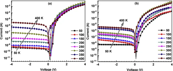
can be used as a thermal detector at reverse biases [30]. Moreover, the doping of the TiO2with Cu caused to increase the current at forward biases by increasing temperature (Fig. 2b).
To obtain device parameters such as barrier height and ideality factor, thermionic emission theory can be performed on the I–V mea-surements. According to this theory, the current (I) is given via the following formula: = ⎛ ⎝ ⎞ ⎠ ⎡ ⎣ ⎢ − ⎛⎝− ⎞⎠⎤⎦⎥ I I V n T V n T exp q k 1 exp q k 0 (1) whereI0is saturation current and determined the intercept value of the
linear portion of lnI-V plot at zero voltage. The q, n, k and T represent charge of the electron, ideality factor, Boltzman's constant and tem-perature, respectively. TheI0is given by following equations according
to thermionic emission theory:
= ⎛ ⎝− ⎞ ⎠ I AA T Φ T * exp q k b 0 2 (2) whereΦb shows the barrier height at zero bias, A and A*are contact area of the device and Richardson constant (A*= 112 Acm−2K−2for n-type Si), respectively. If equations(1) and (2)are rearranged, the n and
Φbare obtained by next formulas:
= ⎛ ⎝ ⎞ ⎠ n T dV dlnI q k (3) and ⎜ ⎟ = ⎛ ⎝ ⎞ ⎠ Φ Tln A AT I k q * b 2 0 (4)
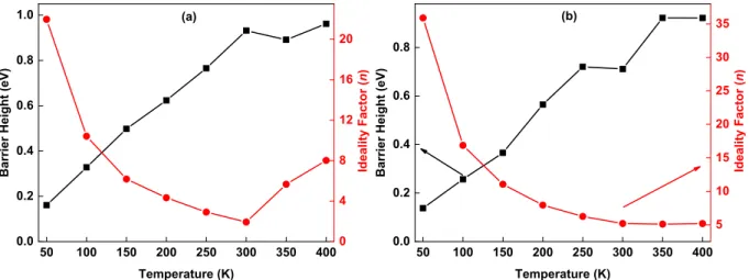
The n andΦbvalues were calculated for the Al/TiO2/n-Si and Al/ Cu:TiO2/n-Si devices by equations of (3) and (4), and tabulated in Tables 1 and 2. Furthermore, Fig. 3a and b shows the temperature dependent profile of the n andΦbvalues of the Al/TiO2/n-Si and Al/ Cu:TiO2/n-Si devices, respectively. While theΦbvalues of the Al/TiO2/ n-Si and Al/Cu:TiO2/n-Si devices almost linearly increased with in-creasing temperature, the n values decreased exponentially. On the other hand, the n values increased after room temperature for the Al/ TiO2/n-Si device. Normally, both n andΦbvalues are not affected by the change of the temperature for Schottky devices. The temperature de-pendence at the n andΦbvalues can be attributed to that the devices have not pure thermionic emission transport mechanism [31]. The deviation from the thermionic emission mechanism can be depended on the barrier inhomogeneities due to the non-uniform interfacial TiO2 layers, its thickness and non-uniform charge distribution between the Al and n-Si [31,32]. Although the devices have high barrier height, flowing of the charge carriers is provided by lower parts of barrier height [33]. This means that the barrier height is not homogeneous, and the device exhibits unstable barrier height and ideality factor values
depending on temperature [34–36]. The barrier inhomogenities can be controlled by uniform and wonderful interfacial layers [37].
All the ideality factor values of the Al/TiO2/n-Si and Al/Cu:TiO2 /n-Si devices at various temperatures are bigger than one. These higher ideality factor values also can be attributed to interface states and barrier inhomogeneity depending on the interfacial layer of undoped and Cu doped TiO2 thin film [38,39]. Furthermore, the saturation current values, which are shown inTables 1 and 2, of the Al/TiO2/n-Si and Al/Cu:TiO2/n-Si devices increased with increasing temperature, but Al/Cu:TiO2/n-Si device has higher saturation current value than the Al/TiO2/n-Si device.
Fig. 4a and b displays the nkT versus kT plot of the Al/TiO2/n-Si and Al/Cu:TiO2/n-Si devices, respectively. nkT-kT plots provide to better understand of the current mechanism for these kinds of devices. In the case of the ideal Schottky device, pure thermionic emission transport mechanism is an effective mechanism [36]. In the pure thermionic emission condition, the barrier height and ideality factor values are not
functions of the temperature, and nkT-kT graphs exhibit a linear plot with unity slope. In our study, the devices are not ideal Schottky device and showed thermionicfield emission behavior associated with ther-mionic emission current transport mechanism. This results confirmed also the barrier inhomogeneity of the devices [40].
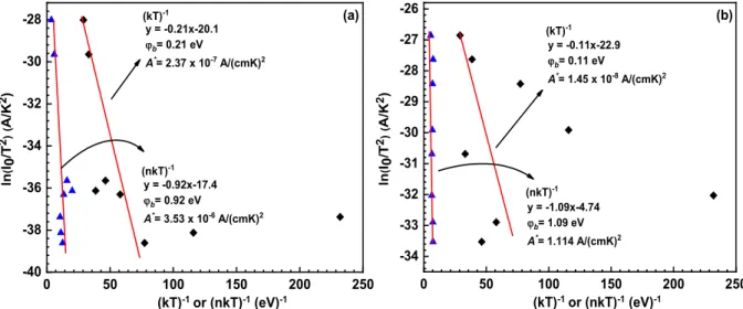
The Richardson or the ln(I0/T2) versus (kT)−1- (nkT)−1plots of the Al/TiO2/n-Si and Al/Cu:TiO2/n-Si devices have been indicated in Fig. 5a and b, respectively. Normally, the Richardson constant of the n-type Si is 112 A/(cmK)−1, but we obtained 3.53 × 10⁻⁶and 1.11 A/ (cmK)−1 for the Al/TiO2/n-Si and Al/Cu:TiO2/n-Si devices as lower Richardson constant than 112 A/(cmK)−1. This case confirms the bar-rier inhomogeneity at the interface of the devices [36]. The Richardson constant of the Al/Cu:TiO2/n-Si device is so higher than that of the Al/ TiO2/n-Si device. This difference may be attributed to increasing charge carriers via Cu doping of TiO2.
The Cheung method can be employed to determine the device parameters as well as series resistance (Rs) of the devices. When the Rs
Fig. 2. LnI-V plots of the a) Al/TiO2/n-Si and b) Al/Cu:TiO2/n-Si for various temperature.
Table 1
The obtained device parameters of the Al/TiO2/n-Si device for the various methods.
T(K) I0Saturation Current n (TE) n (Cheung) Φb(TE) Φb(Cheung) Φb(Norde) Rs(Cheung) (dv/dlnI-I)
(kΩ) Rs(Cheung) (H(I)–I) (kΩ) Rs(Norde) (F(V)–V) (kΩ) RR 50 1.47 × 10⁻¹³ 21.9 24.1 0.16 0.12 0.15 14.1 14.3 3.89 2.01 × 10⁶ 100 2.78 × 10⁻¹³ 10.4 11.4 0.33 0.25 0.31 12.4 11.3 2.52 2.56 × 10⁶ 150 3.83 × 10⁻¹³ 6.18 6.59 0.50 0.39 0.49 11.5 11.0 2.24 1.42 × 10⁶ 200 6.83 × 10⁻¹² 4.33 4.56 0.62 0.53 0.65 6.11 4.65 1.83 3.95 × 10⁵ 250 2.06 × 10⁻¹¹ 2.91 3.18 0.77 0.70 0.77 36.8 22.0 6.36 7.85 × 10⁴ 300 1.83 × 10⁻¹¹ 1.93 2.26 0.93 0.84 0.98 35.6 18.1 3.27 2.49 × 10⁴ 350 1.63 × 10⁻⁸ 5.66 5.44 0.89 0.83 0.88 25.4 21.3 8.21 1.52 × 10³ 400 1.09 × 10⁻⁷ 8.02 8.28 0.96 0.91 0.93 11.9 9.32 9.42 2.70 × 10²
Δn = 0.43 and ΔΦb= 0.0825 eV (average absolute errors).
Table 2
The determined device parameters of the Al/Cu:TiO2/n-Si for the various methods.
T(K) I0Saturation Current n (TE) n (Cheung) Φb(TE) Φb(Cheung) Φb(Norde) Rs(Cheung)
(dv/dlnI-I) (kΩ) Rs(Cheung) (H(I)–I) (kΩ) Rs(Norde) (F(V)–V (kΩ) RR 50 3.07 × 10⁻¹¹ 35.8 50.8 0.14 0.11 0.13 3.06 3.08 1.15 8.68 × 10⁴ 100 1.02 × 10⁻⁹ 16.8 19.6 0.26 0.22 0.24 5.64 5.87 4.43 2.45 × 10⁴ 150 1.02 × 10⁻⁸ 11.0 7.62 0.37 0.34 0.35 0.96 0.76 0.18 2.19 × 10⁵ 200 2.07 × 10⁻¹⁰ 7.94 8.81 0.57 0.48 0.55 2.13 2.15 1.25 1.09 × 10⁴ 250 1.72 × 10⁻¹⁰ 6.25 7.53 0.72 0.59 0.71 0.97 0.88 0.76 1.11 × 10⁴ 300 9.02 × 10⁻⁸ 5.19 5.56 0.71 0.64 0.69 0.42 0.41 0.38 3.10 × 10⁴ 350 5.77 × 10⁻⁹ 5.10 5.93 0.92 0.82 0.92 0.90 0.77 1.76 1.40 × 10³ 400 3.48 × 10⁻⁷ 5.18 4.82 0.92 0.86 0.91 0.58 0.51 0.34 2.76 × 10³
is considered, the current in Eq.(1)is changed by the next form [41]: = ⎛ ⎝ − ⎞ ⎠ I I V IR n T exp q( ) k s 0 (5) This IRscauses the voltage drop for the device. Thus, the Cheung functions are given by the following formula:
= + dV d lnI IR n T ( ) k q s (6) ⎜ ⎟ = − ⎛ ⎝ ⎞ ⎠ ⎛ ⎝ ⎞ ⎠ H I V n T ln I AA T ( ) k q * 2 (7) If Eq(7)are rearranged, the last version of the H(I) are obtained by below relation:
= +
H I( ) IRs nΦb (8)
If both the functions in Eqs.(6) and (8)are plotted against to cur-rent, the linear graphs are obtained in the ideal case. The slopes of these plots provide to determine the two Rsvalues of the device and show the consistency of Cheung method. While the intercept of the dV/d(lnI) versus I plots gives the n values, the intercept of the H(I)–I plots helps to find theΦbvalues of the devices.
The dV/d(lnI)-I and H(I)–I graphs of the Al/TiO2/n-Si and Al/ Cu:TiO2/n-Si devices have been displayed inFig. 6andFig. 7, respec-tively. The obtained n,Φband Rsvalues were listed inTables 1 and 2for the devices. Normally, dV/d(lnI)-I and H(I)–I plots exhibits straight lines, but in this case, the non-ideal device structure and interfacial layers caused to deviate from the linearity. The n values obtained from Cheung method are in good harmony with the n values determined thermionic emission theory for the Al/TiO2/n-Si device (averagely ab-solute errors for n is 0.43), but there are more differences between the n values for the Al/Cu:TiO2/n-Si device at the same temperature (aver-agely absolute errors for n is 3.73). The differences at n values for two devices can be attributed to the Cu doping effect of the TiO2film layer. There are some differences at theΦbvalues depending on the approx-imation differences between the two methods, but the differences are not big for both devices (averagely absolute errors for barrier heights have been shown underTables 1 and 2) [42]. The determined Rsvalues from the dV/d(lnI)-I and H(I)–I plots are close to each other and con-firm the consistency of Cheung method.
Norde method provides to determine theΦb and Rs values as an alternative to Cheung method. According to this method, the Norde function is given via the following formula [43]:
= − ⎛ ⎝ ⎞ ⎠ F V V γ T ln I V AA T ( ) k q ( ) * 2 (9)
whereγrepresents dimensionless integer and greater than n. The I(V) shows voltage dependent current value. The RsandΦb values are ex-tracted from the Norde function and given by the next equations:
= + ⎡ ⎣ ⎢ − ⎤⎦⎥ Φ F V V γ kT q ( ) b 0 0 (10) = − R γ n I T k q s (11) where F(V0) is the minimum point of F(V) and V0is the corresponding voltage.
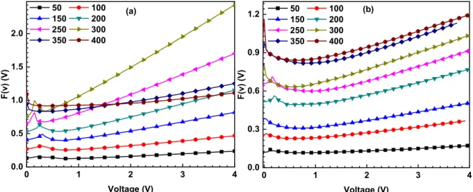
Fig. 8a and b indicate F(v)-V graphs of the Al/TiO2/n-Si and Al/ Cu:TiO2/n-Si devices in the range of 50 K–400 K, respectively. TheΦb and Rsvalues were calculated and listed inTables 1 and 2for the Al/ TiO2/n-Si and Al/Cu:TiO2/n-Si devices from the F(v)-V graphs. TheΦb
file of the n and Φb 2 2
Fig. 4. The nkT versus kT plots of a) Al/TiO2/n-Si and b) Al/Cu:TiO2/n-Si
values are in good agreement with the obtainedΦb values from the thermionic emission theory. The Rsvalues are lower than that of Rs values from the Cheung method for both devices. The reason for dif-ferent Rs values can be attributed to non-ideal device structure and approximation differences [44,45].
We studied temperature dependent profile of interface states density (Nss) for the Al/TiO2/n-Si and Al/Cu:TiO2/n-Si devices. The Nssvalues are obtained from the forward bias I–V measurements by considering efficient barrier height (Φe), ideality factor n(V) and Rs. TheΦeis given by the next formula [46]:
Fig. 5. The experimental Richardson plots a) Al/TiO2/n-Si and b) Al/Cu:TiO2/n-Si devices.
Fig. 6. dv/dln(I)–I plots of a) Al/TiO2/n-Si and b) Al/Cu:TiO2/n-Si devices for various temperatures.
= + − −
Φe Φb (1 1/ ( ))(n V V IRs) (12)
The voltage dependent ideality factor values are calculated by the next equation according to Card and Rhoderick [47]:
= + ⎡ ⎣ ⎢ + ⎤ ⎦ ⎥ n V δ ε ε W qN V ( ) 1 ( ) i s d ss (13) whereδ is the thickness of the layer at the interface (200 nm in this case), εiis permittivity of the interfacial layer, Wdis depletion layer width,εsis permittivity of the semiconductor and Nssexhibits interface state density. If equation (13) rearranged, the Nssis obtained as the following formation: = ⎡ ⎣ ⎢ − − ⎤ ⎦ ⎥ N V q ε δ n V ε W ( ) 1 ( ( ) 1) ss i s d (14)
If the Nssis plotted to conduction band edge of the semiconductor from the semiconductor surface, the energy difference between con-duction band edge and the surface should be calculated by the fol-lowing equation:
− = − −
EC Ess q Φ( e (V IRs)) (15)
The Nssversus Ec– Essplots of the Al/TiO2/n-Si and Al/Cu:TiO2/n-Si devices have been displayed for various temperatures inFig. 9a and b, respectively. The Nssvalues generally shifted to lower band edge with increasing temperature and reached higher values. Fig. 9 clearly
exhibited that the Nssvalues increased after Cu doping to the TiO2layer depending on the increasing defect in the interface. In addition, we can conclude that the Nssvalues are a function of the temperature.
4. Conclusion
We obtained undoped and Cu doped TiO2thinfilms by spin coating technique and employed as an interfacial layer between the Al and n-Si to obtain Al/TiO2/n-Si and Al/Cu:TiO2/n-Si devices. We characterized the Al/TiO2/n-Si and Al/Cu:TiO2/n-Si devices for the temperature range of 50 K–400 K by the I–V measurements. The lnI-V measurements revealed that the currents of the devices are a strong function of the temperature, and the devices can be performed as a thermal detector at reverse biases. Furthermore, the current values of the Al/Cu:TiO2/n-Si device are higher than the Al/TiO2/n-Si device depending on the in-creasing carriers. The device parameters such as ideality factor, barrier height and series resistance were calculated by thermionic emission theory, Cheung and Norde method. The ideality factor values decreased with increasing temperature, the barrier height values increased. The temperature dependence at the barrier height and ideality factor ex-hibited barrier inhomogeneity in the interface of the devices. The series resistance values decreased with increasing temperature. The Al/ Cu:TiO2/n-Si device are lower series resistance than the Al/TiO2/n-Si device. On the other hand, the current transport mechanism of the devices is not pure thermionic emission. The nkT versus kT plots
Fig. 8. F(v)-V graphs of a) Al/TiO2/n-Si and b) Al/Cu:TiO2/n-Si devices in the range of 50 K–400 K.
confirmed that the devices have thermionic field emission with the thermionic emission transport mechanism. The experimental Richardson plots approved that the devices have lower Richardson constant than the real value depending on barrier inhomogeneity. In addition, The Nss versus Ess - Ev plots of the Al/TiO2/n-Si and Al/ Cu:TiO2/n-Si devices showed that Nssvalues almost shifted to lower band edge values with increasing temperature. The results revealed that both the Al/TiO2/n-Si and Al/Cu:TiO2/n-Si devices can be employed in various applications in the wide range temperatures.
Acknowledgments
This work is supported by Selçuk University BAP office with Project Numbers 16401044. Authors would like to acknowledge the support of the Selçuk University for this research.
References
[1] P. Casey, G. Hughes, Photoemission study of the SiO2 conversion mechanism to magnesium silicate, J. Appl. Phys. 107 (2010) 074107, ,https://doi.org/10.1063/1. 3357392.
[2] S. Bhatia, N. Verma, R.K. Bedi, Varied sensing characteristics of in- doped ZnOfilms prepared by sol gel spin coating technique, Int. J. Pure Appl. Phys. 13 (2017) 973–1776http://www.ripublication.com/ijpapspl/ijpapv13n1spl_10.pdf. [3] J.S. Shaikh, N.S. Shaikh, S.S. Mali, J.V. Patil, K.K. Pawar, P. Kanjanaboos,
C.K. Hong, J.H. Kim, P.S. Patil, Nanoarchitectures in dye-sensitized solar cells: metal oxides, oxide perovskites and carbon-based materials, Nanoscale 10 (2018) 4987–5034,https://doi.org/10.1039/C7NR08350E.
[4] M. Yilmaz,Ş. Aydoğan, The effect of Mn incorporation on the structural, morpho-logical, optical, and electrical features of nanocrystalline ZnO thinfilms prepared by chemical spray pyrolysis technique, Metall. Mater. Trans. A 46 (2015) 2726–2735,https://doi.org/10.1007/s11661-015-2875-7.
[5] A. Kocyigit, D. Tatar, A. Battal, M. Ertugrul, B. Duzgun, M. Ertuğrul, A.B. Duzgun, Highly efficient optoelectronic properties of doubly doped SnO2 thin film deposited by spin coating technique, J. Ovonic Res. 8 (2012) 171–178.
[6] C.P. Liu, Y.Y. Hui, Z.H. Chen, J.G. Ren, Y. Zhou, L. Tang, Y.B. Tang, J.A. Zapien, S.P. Lau, Solution-processable graphene oxide as an insulator layer for meta-l–insulator–semiconductor silicon solar cells, RSC Adv. 3 (2013),https://doi.org/ 10.1039/c3ra42967a17918.
[7] C.Y. Liu, H.Y. Xu, Y. Sun, J.G. Ma, Y.C. Liu, ZnO ultraviolet random laser diode on metal copper substrate, Opt. Express 22 (2014) 16731,https://doi.org/10.1364/ OE.22.016731.
[8] M. Yıldırım, A. Kocyigit, Characterization of Al/In:ZnO/p-Si photodiodes for var-ious in doped level to ZnO interfacial layers, J. Alloy. Comp. (2018),https://doi. org/10.1016/j.jallcom.2018.07.295.
[9] I. Orak, M. Toprak, A. Turut, Illumination impact on the electrical characterizations of an Al/Azure A/p-Si heterojunction, Phys. Scr. 89 (2014),https://doi.org/10. 1088/0031-8949/89/11/115810115810.
[10] A. Kocyigit,İ. Karteri, I. Orak, S. Uruş, M. Çaylar, The structural and electrical characterization of Al/GO-SiO2/p-Si photodiode, Phys. E Low-Dimensional Syst. Nanostructures. 103 (2018) 452–458,https://doi.org/10.1016/j.physe.2018.06. 006.
[11] Y.Şafak-Asar, T.T. Asar, Ş. Altındal, S. Özçelik, Ş. Altindal, S. Özçelik, Investigation of dielectric relaxation and ac electrical conductivity using impedance spectroscopy method in (AuZn)/TiO2/p-GaAs(1 1 0) Schottky barrier diodes, J. Alloy. Comp. 628 (2015) 442–449,https://doi.org/10.1016/j.jallcom.2014.12.170.
[12] A. Kumar, S. Mondal, S.G. Kumar, K.S.R. Koteswara Rao, High performance sol–gel spin-coated titanium dioxide dielectric based MOS structures, Mater. Sci. Semicond. Process. 40 (2015) 77–83,https://doi.org/10.1016/j.mssp.2015.06.073. [13] Y.Şafak Asar, T. Asar, Ş. Altındal, S. Özçelik, Dielectric spectroscopy studies and ac
electrical conductivity on (AuZn)/TiO 2/p-GaAs(110) MIS structures, Philos. Mag. 95 (2015) 2885–2898,https://doi.org/10.1080/14786435.2015.1081301. [14] W. Jin, K. Zhang, Z. Gao, Y. Li, L. Yao, Y. Wang, L. Dai, CdSe nanowire-based
flexible devices: Schottky diodes, metal–semiconductor field-effect transistors, and inverters, ACS Appl. Mater. Interfaces 7 (2015) 13131–13136,https://doi.org/10. 1021/acsami.5b02929.
[15] A. Shetty, B. Roul, S. Mukundan, L. Mohan, G. Chandan, K.J. Vinoy,
S.B. Krupanidhi, Temperature dependent electrical characterisation of Pt/HfO2/n-GaN metal-insulator-semiconductor (MIS) Schottky diodes, AIP Adv. 5 (2015) 097103, ,https://doi.org/10.1063/1.4930199.
[16] A. Kocyigit, I. Orak,İ. Karteri, S. Uruş, The structural analysis of MWCNT-SiO2 and electrical properties on device application, Curr. Appl. Phys. 17 (2017) 1215–1222,
https://doi.org/10.1016/j.cap.2017.05.006.
[17] M. Gökçen, H. Altuntaş, Ş. Altındal, S. Özçelik, Frequency and voltage dependence of negative capacitance in Au/SiO2/n-GaAs structures, Mater. Sci. Semicond. Process. 15 (2012) 41–46,https://doi.org/10.1016/j.mssp.2011.08.001. [18] S. Kaya, E. Yilmaz, A comprehensive study on the frequency-dependent electrical
characteristics of Sm2O3 MOS capacitors, IEEE Trans. Electron Devices 62 (2015) 980–987,https://doi.org/10.1109/TED.2015.2389953.
[19] Y. Badali,Ş. Altındal, İ. Uslu, Dielectric properties, electrical modulus and current
transport mechanisms of Au/ZnO/n-Si structures, Prog. Nat. Sci. Mater. Int. 28 (2018) 325–331,https://doi.org/10.1016/J.PNSC.2018.05.003.
[20] E.E. Tanrıkulu, D.E. Yıldız, A. Günen, Ş. Altındal, Frequency and voltage depen-dence of electric and dielectric properties of Au/TiO 2/n-4H-SiC (metal-insulator-semiconductor) type Schottky barrier diodes, Phys. Scr. 90 (2015) 095801, ,
https://doi.org/10.1088/0031-8949/90/9/095801.
[21] A.K. Bilgili, T. Güzel, M. Özer, Current-voltage characteristics of Ag/TiO2/n-InP/Au Schottky barrier diodes, J. Appl. Phys. 125 (2019) 035704, ,https://doi.org/10. 1063/1.5064637.
[22] A. Tataroğlu, A.G. Al-Sehemi, M. Ilhan, A.A. Al-Ghamdi, F. Yakuphanoglu, Optical, electrical and photoresponse properties of Si-based diodes with NiO-doped TiO2 film prepared by sol-gel method, Siliconindia 10 (2018) 913–920,https://doi.org/ 10.1007/s12633-016-9548-z.
[23] M. Yıldırım, Characterization of the framework of Cu doped TiO2 layers: an insight into optical, electrical and photodiode parameters, J. Alloy. Comp. 773 (2019) 890–904,https://doi.org/10.1016/J.JALLCOM.2018.09.276.
[24] F. Bensouici, M. Bououdina, A.A. Dakhel, M. Tounane, A. Iratni, T. Souier, S. Liu, W. Cai, Optical, structural and photocatalysis properties of Cu-doped TiO2 thin films, Appl. Surf. Sci. 35 (2017) 110–116,https://doi.org/10.1016/j.apsusc.2016. 07.034.
[25] Q. Wang, J. Qiao, X. Xu, S. Gao, Controlled synthesis of Cu nanoparticles on TiO2 nanotube array photoelectrodes and their photoelectrochemical properties, Mater. Lett. 131 (2014) 135–137,https://doi.org/10.1016/j.matlet.2014.05.086. [26] G. Blondeau, M. Froelicher, M. Froment, A. Hugot-Le Goff, J. Zerbino, Influence of
copper addition on optical properties of TiO2, J. Electrochem. Soc. 126 (1979) 1592–1596,https://doi.org/10.1149/1.2129337.
[27] D. Dhruv, Z. Joshi, S. Kansara, D.D. Pandya, J.H. Markna, K. Asokan, P.S. Solanki, D.G. Kuberkar, N.A. Shah, Temperature-dependent I–V and C–V characteristics of chemically-grown Y0.95Ca0.05MnO3/Si thinfilms, Mater. Res. Express 3 (2016) 036402, ,https://doi.org/10.1088/2053-1591/3/3/036402.
[28] E. Marıl, A. Kaya, H.G. Çetinkaya, S. Koçyiğit, Ş. Altındal, On the temperature dependent forward bias current–voltage (I–V) characteristics in Au/2% graphe-ne–cobalt doped (Ca3Co4Ga0.001Ox)/n-Si structure, Mater. Sci. Semicond. Process. 39 (2015) 332–338,https://doi.org/10.1016/j.mssp.2015.05.029. [29] İ. Taşçıoğlu, S.O. Tan, F. Yakuphanoğlu, Ş. Altındal, Effectuality of barrier height
inhomogeneity on the current–voltage–temperature characteristics of metal semi-conductor structures with CdZnO interlayer, J. Electron. Mater. 47 (2018) 6059–6066,https://doi.org/10.1007/s11664-018-6495-z.
[30] G. Perez, G. Chicot, Y. Avenas, P. Lefranc, P.O. Jeannin, D. Eon, N. Rouger, Integrated temperature sensor with diamond Schottky diodes using a thermo-sensitive parameter, Diam. Relat. Mater. 78 (2017) 83–87,https://doi.org/10. 1016/j.diamond.2017.08.008.
[31] I. Jyothi, V. Janardhanam, H. Hong, C.-J. Choi, Current–voltage and capaci-tance–voltage characteristics of Al Schottky contacts to strained Si-on-insulator in the wide temperature range, Mater. Sci. Semicond. Process. 39 (2015) 390–399,
https://doi.org/10.1016/j.mssp.2015.05.043.
[32] M. Ali Yildirim, B. Güzeldir, A. Ate, M. Salam, Temperature dependent current-voltage characteristics of the Zn/ZnO/n-Si/Au-Sb structure with ZnO interface layer grown on n-Si substrate by SILAR method, Microelectron. Eng. 88 (2011) 3075–3079,https://doi.org/10.1016/j.mee.2011.05.025.
[33] D.S. Reddy, M.S.P. Reddy, V.R. Reddy, Analysis of current-voltage-temperature ( I-V-T ) and of Pt/Ti Schottky contacts, on n-type InP 5 (2011) 448–454. [34] S. Kumar, Y.S. Katharria, S. Kumar, D. Kanjilal, Temperature-dependent barrier
characteristics of swift heavy ion irradiated Au/n-Si Schottky structure, J. Appl. Phys. 100 (2006),https://doi.org/10.1063/1.2388855113723.
[35] F.E. Cimilli, H. Efeoğlu, M. Sağlam, A. Türüt, Temperature-dependent curren-t–voltage and capacitance–voltage characteristics of the Ag/n-InP/In Schottky diodes, J. Mater. Sci. Mater. Electron. 20 (2009) 105–112,https://doi.org/10. 1007/s10854-008-9635-z.
[36] A. Guzel, S. Duman, N. Yildirim, A. Turut, Electronic transport of an Ni/n-GaAs diode analysed over a wide temperature range, J. Electron. Mater. 45 (2016) 2808–2814,https://doi.org/10.1007/s11664-016-4342-7.
[37] K. Ejderha, N. Yıldırım, B. Abay, A. Turut, Examination by interfacial layer and inhomogeneous barrier height model of temperature-dependent I–V characteristics in Co/p-InP contacts, J. Alloy. Comp. 484 (2009) 870–876,https://doi.org/10. 1016/J.JALLCOM.2009.05.062.
[38] N. Shiwakoti, A. Bobby, K. Asokan, B. Antony, Temperature dependent dielectric studies of Ni/n-GaP Schottky diodes by capacitance and conductance measure-ments, Mater. Sci. Semicond. Process. 42 (2016) 378–382,https://doi.org/10. 1016/j.mssp.2015.11.010.
[39] M.A. Mayimele, J.P.J. Van Rensburg, F.D. Auret, M. Diale, Analysis of temperature-dependant current-voltage characteristics and extraction of series resistance in Pd/ ZnO Schottky barrier diodes, Phys. B Condens. Matter 480 (2016) 58–62,https:// doi.org/10.1016/j.physb.2015.07.034.
[40] M. Özer, D.E. Yıldız, Ş. Altındal, M.M. Bülbül, Temperature dependence of char-acteristic parameters of the Au/SnO2/n-Si (MIS) Schottky diodes, Solid State Electron. 51 (2007) 941–949,https://doi.org/10.1016/J.SSE.2007.04.013. [41] S.K. Cheung, N.W. Cheung, Extraction of Schottky diode parameters from forward
current-voltage characteristics, Appl. Phys. Lett. 49 (1986),https://doi.org/10. 1063/1.9735985.
[42] Ş. Karataş, Effect of series resistance on the electrical characteristics and interface state energy distributions of Sn/p-Si (MS) Schottky diodes, Microelectron. Eng. 87 (2010) 1935–1940,https://doi.org/10.1016/j.mee.2009.11.168.
[43] H. Norde, A modified forward I-V plot for Schottky diodes with high series re-sistance, J. Appl. Phys. 50 (1979) 5052–5053,https://doi.org/10.1063/1.325607. [44] Ş. Karataş, N. Yildirim, A. Türüt, Electrical properties and interface state energy