I
INVESTIGATION OF ELECTRICAL PROPERTIES OF SURFACE STRUCTURES BY X-RAY PHOTOELECTRON SPECTROSCOPIC TECHNIQUE UNDER EXTERNAL
VOLTAGE STIMULI
A THESIS
SUBMITTED TO THE DEPARTMENT OF CHEMISTRY AND THE INSTITUTE OF ENGINEERING AND SCIENCES
OF BİLKENT UNIVERSITY
IN PARTIAL FULFILLMENT OF THE REQUIREMENTS FOR THE DEGREE OF
MASTER OF SCIENCE
By
U. KORCAN DEMIROK February 2005
II
I certify that I have read this thesis and that in my opinion is it is fully adequate, in scope and quality, as a thesis of the degree of Master in Science
……….. Prof. Dr. Şefik Süzer (Principal Advisor)
I certify that I have read this thesis and that in my opinion is it is fully adequate, in scope and quality, as a thesis of the degree of Master in Science
……….. Prof. Dr. Abdullah Atalar
I certify that I have read this thesis and that in my opinion is it is fully adequate, in scope and quality, as a thesis of the degree of Master in Science
……….. Assoc. Prof. Dr. Ömer Dağ
III
I certify that I have read this thesis and that in my opinion is it is fully adequate, in scope and quality, as a thesis of the degree of Master in Science
……….. Assoc. Prof. Dr. Margarita Kantcheva
I certify that I have read this thesis and that in my opinion is it is fully adequate, in scope and quality, as a thesis of the degree of Master in Science
……….. Assoc. Prof. Dr. Ahmet Oral
Approved for the Institute of Engineering and Sciences
……….. Prof. Dr. Mehmet Baray
Director of Institute of Engineering and Science
IV ABSTRACT
INVESTIGATION OF ELECTRICAL PROPERTIES OF SURFACE STRUCTURES BY X-RAY PHOTOELECTRON SPECTROSCOPIC TECHNIQUE UNDER
EXTERNAL VOLTAGE STIMULI
U. KORCAN DEMİROK M.S. in Chemistry
Supervisor: Prof. Dr. Şefik Süzer February, 2005
Electrical properties of surface structures are analyzed using XPS (X-Ray Photoelectron Spectroscopy) by means of external stimuli together with a novel technique allowing the user to record 200 conventional spectra in a period of one second with a time resolution of 5ms.
Charging processes of surface structures such as SiO2 and C12-thiol-capped gold nanoclusters are monitored by time resolved XPS technique which gives an approximate charging constant of the system (RC), and electrical parameters like resistance and capacitance are estimated using external biasing and other relevant time resolved XPS data. Moreover, development and optimization of the technique are carried out by certain parameters and observing the changes in the time constants and binding energy shifts.
It is also shown that application of positive and negative external bias can be used to identify two different forms of gold that exist together in the same sample, as nanoparticles and bulk metal, by means of stimulating the charging-induced-separation of the Au 4f peaks which would otherwise appear as overlapped photoemission signals in the grounded spectrum.
Keywords: SiO2/Si, Charging, External Bias, Time Resolved XPS, Time Constant, Gold Nanoparticles
V ÖZET
DIŞARIDAN VERİLEN VOLTAJ YARDIMIYLA YÜZEY YAPILARININ ELEKTRİKSEL ÖZELLİKLERİNİN X-IŞINI FOTOELEKTRON
SPEKTROSKOPİSİ KULLANILARAK İNCELENMESİ
U. KORCAN DEMİROK Kimya Yüksek Lisans Tezi Danışman: Prof. Dr. Şefik Süzer
February 2005
Çeşitli yüzey yapılarının elektriksel özellikleri XPS (X-Işını fotoelektron spektrumu) tekniği ile ve dışarıdan verilen voltaj yardımıyla, bir saniye içinde 5 milisaniye aralıklarla 200 spektrum alınmasına olanak sağlayan ilk kez tarafımızdan geliştirilmiş yeni bir teknikle incelendi.
SiO2 ve C12-thiol kaplı altın nano-parçacıklarının elektriksel yüklenme süreçleri incelenen sistemin RC sabitinin ölçülmesine olanak tanıyan bu yeni zaman çözünümlü XPS tekniği ile incelendi ve yardımcı başka yöntemler de kullanılarak bu malzemelerin resistans ve kapasitans değerleri tayin edildi.
Bunlarla birlikte bu yeni tekniğin geliştirilmesi ve verimliliğinin arttırılması amacıyla çeşitli parametrelerin değiştirilmesi ve zaman sabitlerine ve bağlanma enerjilerinin kaymalarına etkilerinin gözlenmesi suretiyle çalışmalar yapıldı.
Bunun yanında dışarıdan uygulanan voltajın aynı numune üzerinde bulunan ve topraklanmış XPS spektrumunda üst üste görünen altın metali ve altın nano-parçacıklarından gelen altın 4f sinyallerinin ayrılmasını sağlayabileceği ve neticede bu iki altın şeklinin XPS spektrumunda ayrı ayrı görülebileceği gösterildi.
Anahtar Kelimeler: SiO2/Si, Yüklenme, Dışarıdan Voltaj Uygulanması, Zaman Çözünümlü XPS, Zaman Sabiti, RC Sabiti, Altın Nano-parçacıkları
VI ACKNOWLEDGEMENTS
It is more than a pleasure and an honor to overstate my deepest gratitude here to my dear supervisor Prof. Dr. Şefik Süzer. He has not only been a supervisor to me with his vast knowledge and experience throughout my studies, but also a perfect model both as a person and an outstanding academician in the field. I am very lucky that I have been able to learn such virtues from him that I would thank him for years. I deeply appreciate and would like to thank him endlessly for being an instructor, professor, supervisor and an elder of mine. I would like to extend my kindest gratitude to; Dr. Gülay Ertaş for her company, help and valuable discussions throughout my studies and my very dear friend Burak Ülgüt for his years-long friendship and joyful undergraduate frames that I would not forget. I wish the best for him during all his dear life.
I also would like to thank to former and current Süzer-Lab members; Özgür Birer, Ferdi Karadaş, H. Nezih Türkçü, Ercan Avcı, Ilknur Kaya-Tunç, Bora İnci and Eda Özkaraoğlu for their help and pleasant presence in the lab.
I appreciate the moral support by dear friends; Selim Alayoğlu, Rukiye Karadeniz, Gökhan Arıkan, Ümit Akbal, Anıl Ağıral, A. Faik Demirörs, Nesibe Çındır, Mehtap Küyükoğlu, Oğuzhan Çelebi, Mehmet Göllü, Ethem Anber, Serdar Durdağı, Cenk Tura, Yaşar Akdoğan and Olga Samarskaya.
I am deeply indebted to Bilkent University and the Chemistry Department for providing us such a solid and high-quality education.
Finally, I can not express even a bit of my love and gratitude with strongest words on earth for my very dear mother, father and my dear brother.
VII
TABLE OF CONTENTS
1. INTRODUCTION...1
1.1. X-ray Photoelectron Spectroscopy (XPS) ...1
1.1.1. Principles ...1
1.1.2. Applications ...3
1.1.3. Charging in XPS...7
1.2. External Bias Induced Sample Probing with XPS ...10
1.2.1. Effects on Charging...11
1.3. Time-Dependent XPS measurements ...13
1.4. Oxide-Semiconductor Systems ...15
1.5. Gold Nanoclusters...16
1.5.1. Capped Gold Nanoparticles...16
2. AIM ...18
3. EXPERIMENTAL...19
3.1. Sample Preparation...19
3.1.1. SiO2/Si System...19
3.1.2. Au(foil)/SiO2/Si System...19
3.1.3. Au (TOAB)/SiO2/Si System...20
3.1.4. Au (thiol)/Au(foil)/SiO2/Si System ...20
3.2. Instruments and Techniques...21
3.2.1. XPS ...21
3.2.2. Hardware ...21
3.2.3. Software ...22
3.3. Application of Time Resolved XPS (TRXPS)...25
3.4. External Biasing...25
3.4.1. External Resistance...26
3.4.2. External Capacitance...26
3.4.3. RC Measurements ...26
3.5. Electron Flood Gun ...26
4. RESULTS AND DISCUSSION ...28
4.1. External Biasing Measurements with Si/SiO2 System ...28
4.1.1. The Effect of Low Energy Electron Bombardment ...32
4.2. External Bias Induced Separation of Au-4f Peaks in Si/SiO2/Au(Cluster)/Au (foil) System...34
4.3. TRXPS Results of Various Systems...36
4.3.1. Si/SiO2 System...38
4.3.2. Si/SiO2/Au(nanocluster) System...39
4.4. Effect of Low Energy Electron Gun on Binding Energy Shifts and Time Constants ...45
4.5. Dependence of Time Constant on Photoemission Current ...46
4.6. Variation of Delay Period...47
4.7. Effect of Sample Thickness on Time Constants...51
4.8. Voltage Dependence of Time Resolved Spectra...53
4.8.1. The Effects of Reversing the Polarity of Pulses ...53
VIII
4.9. Elucidation of Electrical Parameters of Surface Structures with External
Biasing...56
4.9.1. Electrical Modeling of Surface Structures ...56
4.9.2. The Use of External Resistance...58
4.9.3. External RC...60
5. CONCLUSIONS ...68
6. References ...71
LIST OF TABLES Table 1. Amount of charging in oxide overlayer together with positive and negative charging with respect to ground. ...12
Table 2. Tabulated values of binding energies of silicon and gold upon application of +6V and -6V ...30
Table 3. Results of different filament currents on the binding energy values and FWHM of silicon oxide grown at 8000C for 7h and bulk gold. ...33
LIST OF FIGURES Figure 1. Formation of Photoelectrons ...1
Figure 2. Two different oxidation states of Si in a 4 nm-thick-SiO2/SiSystem...4
Figure 3. Core level XPS spectra of 1.4nm-thick SiO2 overlayers on Si (100) and Si (111)....5
Figure 4. The relative binding energies of the corresponding oxidation states of silicon with respect to silicon in its neutral state ...7
Figure 5. Charging in a non-conducting sample ...8
Figure 6. The effect of resistance on the binding energy values of gold. ...9
Figure 7. Externally D.C. biased Si/SiO2/Au(foil) System...11
Figure 8. Time-resolved XPS spectra of In 3d5/2 of a) n-InP(110) and b) p-InP(110) after cleaved in UHV27...14
Figure 9. Au(foil)/SiO2/Si System...20
Figure 10. Au (thiol)/Au(foil)/SiO2/Si System...21
Figure 11. A screenshot of the GUI of the program coded in Visual Basic for time resolved XPS measurements. ...23
Figure 12. The setup used in TRXPS measurements...25
Figure 13. Equivalent circuit of the system used for application of low energy electrons inside the vacuum chamber. ...27
Figure 14. Relative differences in energy changes of Gold, which was used as a reference, and SiO2, under +6V and -6V. ...29
Figure 15. The change in binding energy of Silicon with respect to Gold as a function of external bias...31
IX
Figure 16. External bias induced separation of Au 4f peaks in a substrate containing gold both as nanoclusters capped by TOAB and in its bulk state. ...35 Figure 17. An electrical model of the system described above...36 Figure 18. An illustration of the time resolved XPS data acquisition process ...37 Figure 19. TRXPS spectrum of a Si/SiO2 system showing the silicon region. The changes in
Si0 (right) and Si4+ (left) peaks in time are shown together. ...38 Figure 20. The peak maxima of oxide Si2p photoemission versus time. ...40 Figure 21. XPS spectra showing Si2p and Au4f regions taken under +10V and -10V. ...41 Figure 22. Time-resolved XPS spectra of the Si2p-Au4f region of (a) a Si/SiO2 sample
containing a ca. 400-nm oxide layer and a gold metal strip connected to it and (b) the same sample onto which C12-thiol-capped gold nanoclusters are deposited. Charging curves of the two components that are obtained by curve fitting of the individual time resolved XPS data are shown in (c). ...42 Figure 23. Exponential fits of the charging curves for Si2p and Au4f. The shifts are
transformed into decay curves for better fit analysis. ...43 Figure 24.. XPS spectra demonstrating the effect of low energy electron emission on the
binding energies and the time dependent behavior. Rows show spectra taken at different electron emission levels whereas two different pulses are illustrated in two columns. In each of the six graphs, spectra taken under +10V, -10V bias and grounded cases with time resolved spectra at 15ms, 500ms, and 1000ms after the application of the external bias are shown. ...45 Figure 25. The effect of increasing the emission current on the time constants. The step
voltage is -10V to +10V. A first order exponential decay fit is shown in red. ...47 Figure 26. Si2p(oxide)-Si2p(Si substrate) differences are plotted versus time for
measurements performed on the same sample which was approximately 8 nm thick. The pulse was from -6V to +6V and the electron emission (ee) was turned on during the experiments. Delay period is varied between 3s and 9s with 3s increments. ...48 Figure 27. Decay of silicon oxide Si2p peak with time in measurements having different
delay periods. The starting points of the curves are superimposed on each other for a better view of the delay-dependent changes...49 Figure 28. TRXPS results of silicon region of a sample with varied delay periods (a) 1s and
(b) 6 s. The sample was approximately 40 nm thick and the step was -10V to +10V. ...50 Figure 29. FWHM and the Si2p peak position of silicon oxide which is approximately 30 nm
...51 Figure 30. Shift of Si4+ peak maxima and the accompanying changes in FWHM. The sample
...52 Figure 31. Charging and discharging curves for a 20-nm thick SiO2 overlayer under 3.4A low energy electron emission. Voltage steps are indicated in the figure...54 Figure 32. Si2p regions of a thick (ca.400 nm) SiO2 layer showing the charging (b) and
discharging (a) curves in the negative bias region...55 Figure 33. Reversal of the voltage step and the associated changes induced in the charging
process of a thick silicon oxide layer. The current passing through the filament of the electron gun is 3.4A with no floating voltage applied...56 Figure 34. Electrical equivalent of Si/SiO2 system ...57 Figure 35. Connections showing the introduction of a series external resistance to the Si/SiO2
system. ...58
X
Figure 36. The measured binding energy difference between the Si2p peaks of the oxide layer (approximately 4 nm thick) and the silicon substrate plotted against the external voltage bias. The measured binding energy difference between the Au4f peaks with and without 10 MΩ external resistance is also shown in green. The binding energy
difference between the Si2p of the substrate and Au4f does not change. ...59 Figure 37. 200 time-dependent XPS spectra of the Si2p region for the SiO2(4 nm)/Si system
(a’), and the Au4f region of a gold metal strip connected to an external 10 Mohm series resistor and a 56 nF parallel capacitor (b’). The schematics of the two systems are also shown above in a and b. First order exponential fits give time constants of 2 and 0.5 s for the Si/SiO2 and the Au(m) with the external RC circuit respectively. ...61 Figure 38. A simulation of a Si2p peak composed of 10 different smaller peaks. For practical purposes, the small peaks are assumed to be Gaussians of FWHM=1. The data points of the exponential decay curve specify the intensity ratios of the peaks but not necessarily the peak positions...63 Figure 39. Si2p-Au4f differences belonging to outermost 6 layers at two different potentials
are shown. Low energy electron emission (3.4A-4V) was turned on during the
measurements...64 Figure 40. A model illustrating the potential profile of the top 10 nm of a sample upon
application of a positive bias. ...65 Figure 41. A Si2p peak and peak fitting results are shown in a). Relative Si2p peak positions
in three different voltages with respect to gold in b). The photoemission coming from the first three layers under +8V external bias are marked as 1, 2, and 3...66 Figure 42. The binding energy shifts observed in each layer versus external voltage ...67
1
1. INTRODUCTION
1.1. X-ray Photoelectron Spectroscopy (XPS)
XPS (X-ray Photoelectron Spectroscopy) has been one of the leading surface analysis techniques for monitoring surface structures and modifications in the nanometer scale. Based on the photoelectric effect1,2 XPS was developed in mid-1960’s by Kai Siegbahn and his research group at the University of Uppsala, Sweden.3
In general use of XPS, binding energies of the electrons that are emitted from different atomic levels of various elements are measured via which all chemical information is derived.4 Thus, composition of the surfaces, chemical states of the components and charging behavior of the surfaces are obtained through XPS analysis.
1.1.1. Principles
Figure 1. Formation of Photoelectrons
By means of an incident X-ray irradiation which is directed towards the sample, photoelectrons are emitted and kinetic energies of the photoelectrons emitted from the sample are measured in the electron energy analyzer, which, in turn, gives the binding energy
photo-electrons
X-rays
Sample
2
of the corresponding electron. This analysis yields the elemental composition of the outermost layers that are in question.
The X-ray photoemission process is governed by the equation,
BE=hν-KE-Φ (1)
where hν is the energy of the incident photon, BE is the binding energy, KE is the kinetic energy of the electrons emitted and Φ is the work function of the sample and the instrument.
To a great extent, the electrons detected by the analyzer during a photoemission process are from the outermost layers (<10 nm). Although X-rays can penetrate deeper (~1μm) into the material to create photoelectrons, these electrons can not survive since they lose most of their energies during inelastic collisions throughout the way to the surface of the material. Inelastic mean free path (), which is a measure of the distance traveled by a photoelectron inside the sample, is an important indication of the possibility that a given photoelectron can end its trajectory up with the detector5 and is defined as I/I0=e-1. The reason why XPS is such a surface sensitive technique is that the electrons, which have enough energy to travel more than 3, can reach the analyzer and constitute a signal where is in the range between 0.4 nm and 4 nm. Therefore the signals are obtained from the outermost 10-12 nm of the sample in question. However, it is possible to further increase the surface sensitivity by means of Angle Resolved XPS.6-7
3
1.1.2. Applications
XPS can be used for a wide variety of applications; chemical analysis being the most frequently used one.
1.1.2.1. Chemical Analysis
Although the X-ray photoemission process is not as strong as the photoemission process in Ultraviolet Photoelectron Spectroscopy, it is powerful enough for precise analysis at molecular levels regarding chemical compositions of surface structures.
Besides qualitative information obtained by XPS on elemental compositions of substrates analyzed, the relative atomic ratios of the components can also be found by appropriate analysis of the resulting XPS spectrum such that,
(6)
where X/Y is the atomic ratio of species X to species Y in the sample, A is the area of the corresponding peak in the spectrum, is the photoionization cross-section and EK is the kinetic energy of the corresponding peak.
Besides its use in elemental differentiation, XPS also gives information on the chemical state of a particular atom. Since the chemical state of an atom creates a unique potential around the photoelectron ejected, the kinetic energy of the photoelectron in question is affected by the surrounding potential. This increase or decrease in the kinetic energy of the
2 / 3
)
(
)
(
X K Y K X Y Y XE
E
A
A
Y
X
4
photoelectron, which is termed as chemical shift, relative to the neutral atom gives information on the chemical state of the atom in question.
1 0 8 1 0 6 1 0 4 1 0 2 1 0 0 9 8 B i n d i n g E n e r g y ( e V ) S i0 S i4 + 4 n m S i O 2/ S i
Figure 2. Two different oxidation states of Si in a 4 nm-thick-SiO2/SiSystem
In Figure 2, Si in its neutral and 4+ oxidation states are represented by two separated peaks in the spectrum.8 Due to positive environment around the electron to be ejected by an X-ray in Si4+, photoelectrons from Si4+ are shifted towards higher binding energies in the energy scale. Likewise, photoelectrons ejected from a negative environment would produce a shift towards lower binding energy values.
5
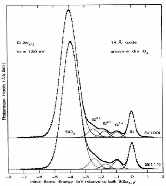
Figure 3. Core level XPS spectra of 1.4nm-thick SiO2 overlayers on Si (100) and Si (111)
In the work of Himpsel et.al.9, four different oxidation states of silicon and its neutral form, namely, Si0, Si1+, Si2+, Si3+, and Si4+, in Si (100) and Si (111) substrates are displayed together in high resolution XPS spectra. The spectrum was recorded at 130eV photon energy which belongs to a 0.5 nm oxide overlayer that was grown in 2x10⁻⁵ Torr at 7500C to show that interfacial states with different oxidation states exist between the bulk silicon and the
6
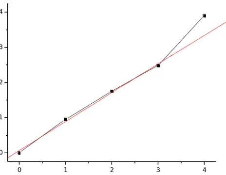
oxide. The relative intensities of these states are shown to be different in Si (100) and Si (111) and are explained by differences in interfacial structures in these two forms. However, the effect of oxygen pressure on the growth of interfacial states and the intensities observed in XPS spectra are shown to be more or less the same for different pressure values between 2x10⁻⁵ Torr to 0.1 Torr. Moreover, the thickness of the oxide film, as in the case of the pressure of oxygen, also does not influence much the relative ratios of energies of +1, +2, +3 states of silicon to Si0. This was demonstrated by growing a 1.4nm thick oxide layer on both Si (100) and Si (111) substrates at 0.1 Torr O2. It is also noticed that the energies of the Si2p photoemission coming from +1, +2 and +3 states are closer to Si0 rather than being evenly distributed between the S4+ and Si0. This shows that although the oxidation states are increased one by one going up from Si0 to Si4+, the overall potential around these structures is not just determined barely by the oxidation state itself but also by the local environment. The fact that an oxidation state of an atom does not directly refer to its charge transfer properties is in parallel with the above statement. Therefore also adding the enhancement of photoionization cross section of higher-oxidation states into account9, it can be inferred from the spectra that +1, +2 and +3 states are in a more partially negatively charged medium than the +4 state. The relative binding energies of the interfacial states versus the charge of silicon is plotted in Figure 4. It is seen that up to Si4+, the values show almost a prefect linear dependence with an R2 value of 0.996 within experimental limits with +4 state slightly being deviated from the derived linear dependence.
7 0 1 2 3 4 0 1 2 3 4 P o s it io n w .r .t . S i 0 ( e V ) Charge of Six+
Figure 4. The relative binding energies of the corresponding oxidation states of silicon with respect to silicon in its neutral state
1.1.3. Charging in XPS
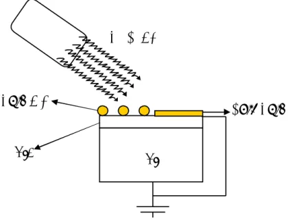
In XPS, charging is the phenomena during which a positive charge develops in the substrate under X-ray irradiation due to lag of replenishment of the ejected electrons. In non-conducting samples, as shown in Figure 5, since photoelectrons are emitted faster than the rate of replenishment from the ground, a positively charged environment is created, which in turn affects the binding energy of the ejected photoelectrons. The kinetic energies of the photoelectrons that reach the detector are lowered due to the extra electrostatic attraction that takes place between the electron and its environment during photoemission process. Possible charging behavior is prevented in conducting samples via grounding the sample. In this case,
8
the emission of a photoelectron is quickly followed by insertion of another electron coming from the ground inside a hole almost immediately (t<10-9s).
Figure 5. Charging in a non-conducting sample
The charging process can be simulated artificially in a conductor which normally would not charge. Suzer’s group has induced positive and negative charging in a gold sample by addition of an external resistor. The sample is then put under a series of positive and negative external voltages to follow the corresponding changes in the Au4f peak maxima. The binding energy differences between the original gold peak and the peak that belongs to gold plus the external resistance are then plotted. As it is also shown below, the binding energy values of Au4f coming from Au+20MΩ system was found to be higher than the original Au4f in the negative bias region (including ground) due to the resistive element in the circuit restricting the movement of electrons and causing the gold to feel and extra positive potential. Likewise the Au+20MΩ system is found at lower binding energies than the original gold in positive bias region which means that the electrons that move from the
Radiation
Photo-electrons
+
+ +
9
sample to the source are now slowed down with the resistor causing an extra negative potential around gold.
-40 -20 0 20 40 -2.0 -1.5 -1.0 -0.5 0.0 0.5 1.0 1.5 B .E . D if fe re n c e ( e V ) Bias Voltage (V) (Au4f+20M) - Au4f
Figure 6. The effect of resistance on the binding energy values of gold.
Although charging has generally been considered as a problem preventing accurate determination of binding energies of various components in non-conducting samples10,11,12, ,13
, it has also been used as a useful tool for various applications in the case of samples containing heterogeneous surface structures.14,15,16,17 Differential charging18,19, which results due to differences in charging behavior of layers/components inside the same medium under same conditions, is also another parameter which has been under extensive investigation. Relative charging differences that exist inside a sample having a varying composition of
10
different atoms or even among the identical elements in a medium which vary only in their morphology allow the investigator to benefit from this differential charging information.20,21
In a recent study by Suzer21, silicon peaks that belong to a PDMS overlayer deposited on top of a SiO2 layer are separated, which otherwise would appear as overlapped features, by making use of differential charging. Upon biasing the system at -5V, first spectral features of Six+ coming from PDMS layer are seen by fitting the peaks in the corresponding region of the XPS spectrum. Si2p photoemission coming from PDMS is further separated from the one coming from SiO2 in the case of -10V negative biasing.
Charging is often handled with referencing and neutralization by low energy electrons. A specific photoelectron peak of known value can be used to calibrate the spectrum. Generally, C1s peak coming from the contamination of a surface or the Au 4f peaks placed in contact with the sample serve as references. The second solution, i.e. neutralizing by electron flood gun, have been extensively used to employ low energy electrons to replenish the ejected photoelectrons.22,4
When combined with information derived from differential charging, external basing8,23, is another important technique in the analysis of surface structures by XPS.
1.2. External Bias Induced Sample Probing with XPS
As mentioned earlier above, external biasing has proven to be a simple yet informative tool8 in XPS analysis of various surface structures. In general, the sample is biased with a positive or negative D.C. voltage to induce voltage dependent shifts in XPS spectra.
11
Figure 7. Externally D.C. biased Si/SiO2/Au(foil) System
In Figure 7, a semiconductor/oxide/metal system, i.e. Si/SiO2/Au(foil), is shown, which was put under -10V and +10V external bias, together with a grounded spectrum. Gold 4f peaks were selected as references and Au4f photoemission in all three spectra were superimposed in the same graph. Si2p coming from the bulk Si is not visible since oxide is thick, ca~200 nm.
1.2.1. Effects on Charging
External bias can be useful in understanding the mechanisms involved during the process of surface charging. It is visible from Figure 7 that without exact energy determination, the absolute amounts of positive and negative charging of Si with respect to Au are different from each other meaning that the differential charging of SiO2 under positive and negative biasing are different in each case, although the absolute value of the voltage
1 1 0 1 0 5 1 0 0 9 5 9 0 8 5 8 0 5 0 0 1 0 0 0 1 5 0 0 2 0 0 0 2 5 0 0 3 0 0 0 3 5 0 0 C o u n ts B .E . ( e V ) + 1 0 V - 1 0 V G ro u n d A u 4 f S i 2 p
12
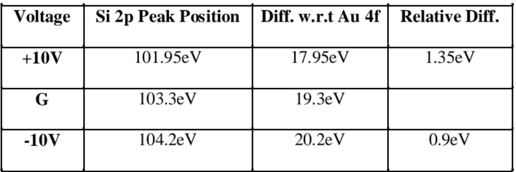
applied is the same for both. Peak positions and corresponding differences are illustrated in Table 1.
Voltage Si 2p Peak Position Diff. w.r.t Au 4f Relative Diff.
+10V 101.95eV 17.95eV 1.35eV
G 103.3eV 19.3eV
-10V 104.2eV 20.2eV 0.9eV
Table 1. Amount of charging in oxide overlayer together with positive and negative charging with respect to ground.
As it is seen from Table 1 that the Si2p photoemission exhibits a shift of 1.35eV with respect to ground under positive D.C. bias where the shift reduces to 0.9eV displaying a 0.45eV decrease in shifts due to charging when the system is under the negative D.C. biasing. This change in the differences between ground and the corresponding peak positions of positive and negative D.C. bias is attributed to differences in neutralization efficiency of stray electrons in these two cases in one of the detailed studies of Karadas et. al.23 on differential charging. In the case of negative bias, the stray electrons are repelled by the surface causing the Si2p shift to be greater than in the case of positive bias. However, upon application of positive bias, the stray electrons are attracted to a greater extent to the sample causing an over-neutralization and resulting in a decrease in the shift of Si2p photoemission to relatively a lower binding energy value than the ideal expected shift of +10V.
13
In addition to the information obtained by external biasing on the nature of charging in various systems, one can use external biasing to deduce other useful chemical or structural information. In one previous application of external bias Havercroft et al. reported that they have been able to use negative external bias to identify chemical differences in oxide films on an aluminum alloy.24 In another study25, we applied positive and negative external bias to separate the photoemission peaks of two different forms of gold, i.e. bulk and capped nanoparticles, which would otherwise be seen as overlapped features in the case of conventionally grounded sample probing. The details of this work will be discussed later in this text.
1.3. Time-Dependent XPS measurements
XPS is generally used to extract chemical information from the sample on its composition or other parameters which does not vary in time. The main reason for this type of ‘restricted’ use is due to the complexity and difficulty of probing dynamic systems which are far from equilibrium. Moreover, the average period that one can obtain decent spectrum is of the order of minutes. Therefore XPS is seldom used to probe fast processes on surfaces.
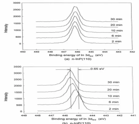
What is generally meant up to this thesis work by time-dependent or time-resolved XPS is merely the acquisition of consecutive several-minute-long XPS spectra one after another, taking minutes, hours, or days to complete, for monitoring the changes that take place on the surface.26 One example to these ‘time-resolved’ measurements is the work by Deng et. al.27, in which GaAs(100) and InP(100) samples were cleaved in UHV to have (110) surfaces. Upon this cleavage the energy band changes in these samples were studied in a timely manner by high resolution XPS.
14
Figure 8. Time-resolved XPS spectra of In 3d5/2 of a) n-InP(110) and b) p-InP(110) after cleaved in UHV27
Consecutive XPS spectra of In 3d5/2 photoemission from n- and p-InP(110) is displayed above to show the changes that occur in the peak position of In 3d5/2 in time. A minimum period of four minutes exists between each spectrum which is the time-resolution in this experiment. Details can be found in the article.27
By changing the conventional way of controlling the instrument, acquisition of time-resolved XPS spectra with 5ms of time resolution is the main emphasis of this thesis which will be discussed later in detail in the text.
15
1.4. Oxide-Semiconductor Systems
Metal-Oxide-Semiconductor systems have been of particular interest to various scientific and industrial communities due to their applications in chip technology.28,29,30,31,32
The first uses of MOS systems date back to 1960’s while 1980’s and 1990’s being the years during which extensive studies on characterization design and development of metal-oxide-semiconductor systems took place.34 Ge instead of Si was used in the preliminary stages of MOS circuits. However, due to its enhanced material properties and wider applicability, Si replaced Ge almost completely later on.
Most of the MOS systems are designed to be used in computers.33 Various MOS systems have been employed in chip industry to achieve the desired electronic properties and the smallest size possible.34 Besides the use of silicon as semiconductor in a MOS system, other attempts to use SiGe mixtures have also been employed.
The importance of Metal/SiO2/Si System in MOS systems lies in its stability, ease of production and promising electronic properties.35 Unlike in the case of compound semiconductors such as GaAs or InP, Si does not decompose under certain processes during production steps. Although the mobility in Si is lower than the mobility in Ge, Si can be operated at higher temperatures without degradation and has a higher band gap than Ge. Moreover by simple thermal processes SiO2, which is a high quality insulator, can be grown readily for many purposes including protection of underlying circuitry and patterning.
It is projected in 1999 edition of International Technology Roadmap for Semiconductors that the CMOS devices must be scaled below 100 nm in the very near future.36 However, with today’s technology it is very difficult to manufacture CMOS devices with sizes below 100 nm. The main problem is the unavailability of current top-down
16
lithographic techniques to produce defect-free sub-100 nm chips. Therefore the future of smaller MOS circuits and the chip industry are seen behind the realms of bottom-up approaches like self-assembly.37
1.5. Gold Nanoclusters
Various forms of gold nanoparticles most of which have been deposited over SiO2 are used throughout our studies. Among these, citrate capped, TOAB (Tetraoctylammoniumbromide) capped and thiol capped ones will be ones to be described. Electrical properties, charging behavior and other structural parameters of the corresponding gold nanoclusters were studied during external biasing and TRXPS (Time resolved x-ray photoelectron spectroscopy) measurements.
1.5.1. Capped Gold Nanoparticles
Formation and preparation of capped Au nanoclusters mostly rely on the electrostatic forces that exist between the clusters and the capping agent. One of the earliest attempts to synthesize capped gold nanoparticles belongs to Turkevich et al.38 which employed trisodiumcitrate to surround the aqueous AuCl4- anions with citrate groups.
1.5.1.1. Citrate-Capped Gold Nanoparticles
Upon heating these two ingredients at moderate temperatures (600C-800C), capped gold particles having a mean radius of 8 - 10 nm were prepared in Turkevich’s studies.38 These particles are characterized by UV-Vis, TEM and electrophoresis measurements. It is
17
shown that typically the particles exhibit a UV-vis peak at 523 nm. Upon increasing the size of the gold clusters, this peak is shown to be shifted to higher wavelengths.39,40,41
1.5.1.2. TOAB-Capped Gold Nanoparticles
TOAB was reported to be used as a PTA (Phase Transfer Agent) in a study by Cheng et. al.42 recently. The transfer of Au nanoparticles from water to toluene was employed. The particles were prepared totally on the principle of electrostatic attractions between TOA+ (Tetraoctylammonium cation) and negatively charged tannic or citrate stabilized gold nanoparticles. These charged structures were of particular importance in determination of effects of positive and negative charging as well as time constant measurements with TRXPS.
1.5.1.3. Thiol-Capped Gold Nanoparticles
Thiol capped particles were also prepared with similar procedures with other capped particles which are deposited from aqueous solution except the steps involving the incorporation of sulphur atoms to gold-bonded ends of C12-alkyl chains upon addition of small amounts 1-dodecenethiol to the solution as described in the work of Brust et. al.43 The potential changes in conductance behavior and electrical properties as well as charging of the new capped gold nanoclusters also fall in the scope of this work.
18
2. AIM
Previous studies8,44 in Suzer’s group have displayed the characteristics of charging under external bias in systems like Si/SiO2, Al/ Al2O3 and W/WO3 and contributed much to understanding the nature and mechanisms of charging in these systems which are of significant importance to many applications in electronic circuitry and computer industry as well as in scientific community.
However, investigation of these systems and observations of binding energy shifts and charging parameters before and after the application of external biasing could have been understood better with the possibility of monitoring the dynamics of the processes mentioned. Starting from this point, the primary objective of our studies was to find a way to disclose how the charging of a system under external bias proceeded in time. For this purpose, we have developed a novel technique and investigated the charging of a Si/SiO2/Au(m) system by XPS with 5ms time resolution between two consecutive XPS spectra.
Application of the technique to other systems like gold nanoclusters deposited on SiO2 and investigation of electrical and material properties of these systems were also of particular interest.
19
3. EXPERIMENTAL
3.1. Sample Preparation
3.1.1. SiO
2/Si System
Mostly, p-doped silicon having (100) orientation is used throughout the studies as the starting material in samples containing Si. Appropriate size of a Si substrate was cut from bigger silicon wafers and put in concentrated HF solutions for 1-2 minutes to be cleaned from already-existing oxides and other surface contaminations. Washing with distilled water and ethanol and/or acetone before drying was performed after ejection from HF solution. SiO2 on Si substrates were grown thermally in furnace under desired temperature for variable amount of time. Thinner oxides were grown at 500-6000C for 3-5 hours where thicker ones were prepared under elevated temperatures, ~8000C, and left in the furnace for several hours, i.e. ~6-12. Thicknesses of the oxide layers are determined from XPS data if the sample contains an oxide layer less than 10nm. Thicker samples are identified via Dektak measurements by etching a part of the oxide and taking the difference between the oxide layer and the Si substrate.
3.1.2. Au(foil)/SiO
2/Si System
In addition to the SiO2/Si system mentioned above, a gold foil is attached to the rod as well. An overall scheme of the resulting setup is illustrated below in Figure 9.
20
Figure 9. Au(foil)/SiO2/Si System
3.1.3. Au (TOAB)/SiO
2/Si System
TOAB capped gold nanoparticles were prepared by the following procedure. 0.4 mL of 0.13 M TOAB (toluene) solution was mixed with 0.4 mL of the 10-4 g/mL aqueous gold nanoparticle solution and stirred.42 It is observed that gold nanoparticles moved from the water layer to the toluene layer.
A few drops of TOAB solution was dripped onto the SiO2/Si substrate and evaporated to form TOAB capped Au nanoparticles on SiO2/Si. TOAB capped gold nanolcusters are analyzed both with and without a gold foil attached onto the Si substrate.
3.1.4. Au (thiol)/Au(foil)/SiO
2/Si System
Using the procedure described in reference 43, gold nanoclusters surrounded with C12-thiol groups are prepared.43 In addition to the nanoclusters deposited on SiO2 by evaporation decribed above, Au foil is also attached to the rod for mainly referencing purposes. The resulting setup is depicted in Figure 10.
Gold
SiO
2Si
x-rays
21
Figure 10. Au (thiol)/Au(foil)/SiO2/Si System
3.2. Instruments and Techniques
3.2.1. XPS
All of the XPS spectra were taken with a KRATOS ES300 X-ray Photoelectron Spectrometer with a non-monochromatized MgK source (1253.6 eV). Pressure of the analysis chamber was kept around 10-9-10-8 Torr. For peak fitting in still and time-resolved measurements, XPSPeak95 v2.0 is employed.
3.2.2. Hardware
Two AD/DA cards (ADA2110 of Real Time Devices Inc. and Super 16-Bit AD/DA of Industrial I/O Cards) are used in data acquisition along with an integrated timer card. One of the AD (28 µs) / DA (2 µs)’s was a 16-bit DAQ card with eight analog inputs and 2 analog outputs. The other AD (20 µs) / DA (10 µs) used had 12-bit analog output resolution with a
Bulk Gold
SiO
2Si
x-rays
Gold N.C.
22
16-bit timer card having an 8MHz internal oscillator. A Pentium-II is used to administer the data acquisition.
3.2.3. Software
Time resolved XPS measurements were recorded with home-made software which was coded in Visual Basic in our labs. Other XPS spectra were taken by a program designed for conventional XPS analysis.
3.2.3.1. Visual Basic
Except for the module which governs ‘read/write’ operations directly by taking advantage of a dynamic link library code, no special modules/sub-modules/macros or predefined codes were used. The entire program was coded in Visual Basic 5.0.
3.2.3.2. The Program
The program uses two analog output channels, one analog input, built-in analog-to-digital analog-to-digital-to-analog converters and three programmable timer-counters simultaneously to control the spectrometer during data acquisition and has a simple yet friendly graphical user interface (GUI). The GUI of the program is shown below in Figure 11.
23
Figure 11. A screenshot of the GUI of the program coded in Visual Basic for time resolved XPS measurements.
As it is also seen in the screenshot of the program above, the program accepts several parameters from the user. In the upper row, under ‘accumulations’ tag, the number of cycles that the program will perform the monitoring process is entered. Next to ‘accumulations’ tag, the desired time resolution between two consequent spectra is requested from the user. The data field on the right in the upper row is the total time during which the charging process is being monitored. The first two fields in the second row are the start and end points which specify the energy frame for the measurement where the field on the right is the energy resolution.
3.2.3.2.1. The Logic
The logic simply lies behind the following idea. Instead of imposing a bias on the sample and shifting the whole energy frame to see the desired peak in its new position
24
afterwards, individual binding energy values that belong to the desired energy frame in which the peak will appear after the application of the bias is monitored immediately after the application of the bias. The process is repeated until all the energy steps that fall into the frame to be monitored are completed.
3.2.3.2.2. The Code
The incorporation of the above logic to a computer code is relatively simple for an intermediate programmer. One of the analog outputs governs the sample voltage while the other is responsible for the energy axis. The code orders the spectrometer to ‘sit’ at a specified binding energy value and tracks the changes in the intensity while the sample voltage is repeatedly altered between two selected bias voltages. Each of the intensity changes are recorded in the meantime with appropriate energy information and stored in a data array to speed up the functioning of the program. The array is then written to a file at the end of the data acquisition.
3.2.3.2.3. Pulse Counting
Electron pulses are counted with integrated programmable timer-counter card. One of the 16-bit timer-counters was referenced to the internal 8MHz oscillator and employed to keep the real time in milliseconds. The second one was used particularly for time keeping in a stopwatch manner to govern the individual pulse counting periods. The last one, working in sync with the second one, was used in the detection of the pulses.
25
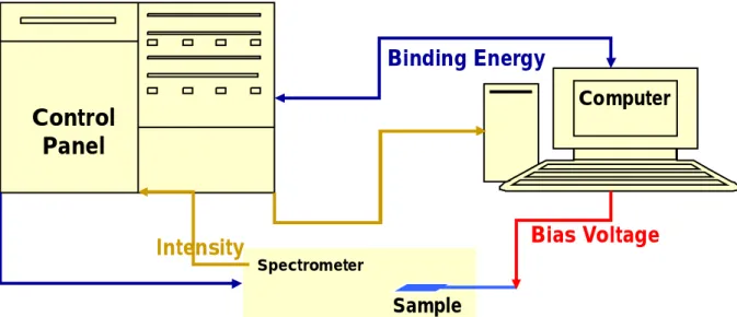
3.3. Application of Time Resolved XPS (TRXPS)
Figure 12. The setup used in TRXPS measurements
As displayed above in Figure 12, application of the computer controlled bias voltage required one more connection from the computer to the sample in addition to conventional connections that are required to obtain a normal XPS spectrum.
3.4. External Biasing
All bias voltages were simply applied to the sample rod which carried the sample by corresponding power supplies. Si was directly in touch with the voltage supply through the rod during still measurements. In the cases when a gold foil is used, the foil was also contacted with the rod as in the case of Si. Analog output of the AD/DA card was connected to the sample rod in the case of TRXPS measurements.
Computer
Control
Panel
Spectrometer Sample Binding EnergyIntensity Bias Voltage
26
3.4.1. External Resistance
Various ohmic resistances ranging from a few ohms to a few hundredths of mega-ohms were used throughout the studies all of which were connected in series to the sample rod.
3.4.2. External Capacitance
Since connecting a capacitor in series without another element to the sample means nothing but an open circuit, the capacitors were connected in parallel with other circuit elements, particularly resistors. Capacitance values of the capacitors were changing from pico farads to micro farads depending on the desired RC values.
3.4.3. RC Measurements
Resistances and capacitors which are connected in parallel with each other but in series with the sample are used for RC measurements.
3.5. Electron Flood Gun
The gun is composed of a tungsten filament which emits electrons inside the vacuum upon passing a current through its ends. The current was controlled with a variable current-voltage power supply. The filament current was varied between 3-3.6A throughout the measurements. When needed, the filament was floated with a few (-) volts ranging from 0 to -6Volts with another D.C. power supply. The overall picture illustrating the setup for supplying extra low energy electrons to the system is shown in Figure 13.
27
Figure 13. Equivalent circuit of the system used for application of low energy electrons inside the vacuum chamber.
I
Filament
Current
Source
V
file
-V
extSample
28
4. RESULTS AND DISCUSSION
4.1. External Biasing Measurements with Si/SiO
2System
As explained earlier in the introduction part, upon application of a fixed magnitude of positive and negative bias to Si/SiO2 system, corresponding shifts induced in oxide Si2p photoemission towards higher and lower binding energies are not the same in magnitude. Thus, one observes a lesser shift to a higher binding energy under negative charging, i.e. positive biasing, where again a lesser shift to lower binding energies in the case of positive charging, i.e. negative biasing, is observed. This asymmetric behavior is attributed to the differences in the mechanisms of positive and negative charging.8
The value of this differential shift was found to be dependent on the magnitude of the bias and it was shown that it saturates after 10V.8 Therefore, to cover the range that responds most to the applied biasing in terms of observed shifts in binding energies, the experiments were mostly carried out within ±10V.
As also displayed in Figure 9, gold was connected on top of Si/SiO2 layer for referencing purposes. Being a perfect conductor, gold, as in many other previous XPS studies, was introduced to determine the amount of charging in SiO2 layer under external bias accurately. It is observed that gold indeed displays exactly the same amount of shifts as the applied external bias within the detection limit of our instrument which is ±0.1eV.
29 120 110 100 90 80 70 0 1000 2000 3000 4000 5000 6000 7000 8000 9000 In te n s it y ( C o u n ts ) B.E. (eV) +6V -6V 11.7eV 12.04eV
Figure 14. Relative differences in energy changes of Gold, which was used as a reference, and SiO2, under +6V and -6V.
Figure 14 implies that Au 4f peaks exhibit a shift of 12.04eV which is almost exactly the total amplitude of the biasing. However, the difference between two Si2p peaks is about 11.7eV. This 0.34eV difference is significant and well above the detection limit providing the driving force for carrying out external bias and differential charging measurements.
Instead of taking the difference between two Si2p peaks in two different cases of external biasing, the difference of Si2p with respect to reference, i.e. gold, is taken throughout our studies to track the changes in charging of SiO2.
30
Voltage Si 2p B.E. (eV) Si 2p FWHM (eV) Au 4f B.E. (eV) Si2p-Au4f
+6V 109.88eV 1.69eV 89.84eV 20.04eV
-6V 98.18eV 1.64eV 77.8eV 20.38eV
Table 2. Tabulated values of binding energies of silicon and gold upon application of +6V and -6V
The binding energies of gold and silicon at -6V and +6V and FWHM values of silicon at these two voltages are shown in Table 2. The full width of Si2p peak at its half maximum (FWHM) does not change much in this case.
31 - 2 0 - 1 0 0 1 0 2 0 1 9 .8 1 9 .9 2 0 .0 2 0 .1 2 0 .2 2 0 .3 2 0 .4 2 0 .5 S i2 p -A u 4 f B .E . D if f ( e V ) B i a s V o l ta g e ( V )
Figure 15. The change in binding energy of Silicon with respect to Gold as a function of external bias.
Si2p-Au4f binding energy difference is plotted versus external bias in Figure 15. The oxide in this sample was grown at 6000C for 3-4 hours and the thickness of the oxide is estimated to be around 10 nanometers. Voltage dependence of the observed shifts is clearly seen in the above figure that as the magnitude of the voltage increases, the binding energy difference between Si2p and Au4f deviates either above or below from its reference value, i.e. the value found upon grounding the system. The positive voltage simply alters the amount of electrons attracted to the sample and thereby controls the negative charging process on the surface. Conversely, a negative voltage again alters the amount of electrons that help surface neutralize, but in the opposite way.
32
One can easily recognize the immediate saturation around -2 Volts while going towards increased negative bias. This behavior is attributed to the easiness of repelling low energy stray electrons even at low negative voltages such as -2-3V. In the case of positive biasing however, the difference saturates at a considerably higher voltage value, around 15V meaning that nearly all of the stray electrons that could help the sample charge negatively are attracted to the surface and the sample can not be neutralized further more by means of an increased positive potential.
4.1.1. The Effect of Low Energy Electron Bombardment
In the case of negative charging, it was also shown in Table 2 that the difference between Si2p and Au 4f decreases. As also mentioned in the work of Ülgüt and Süzer8, stray electrons that are attracted towards the sample surface are shown to be the primary cause of this neutralization. The filament acts as an additional low energy electron gun. The current passing through the filament of the electron gun and the energies of the emitted electrons determined by floating the filament are varied to study the effects on the corresponding shifts.
33
Voltage Si 2p B.E. (eV) Si 2p FWHM (eV) Au 4f B.E. (eV) Si2p-Au4f
+6V-As is 109.88eV 1.69eV 89.84eV 20.04eV
+6V-3.4A 108.89eV 1.91eV 89.82eV 19.07eV
+6V-3.6A 108.59eV 2.05eV 89.81eV 18.78eV
-6V-As is 98.18eV 1.64eV 77.8eV 20.38eV
-6V-3.4A 98.2eV 1.73eV 77.81eV 20.39eV
-6V-3.6A 98.18eV 1.78eV 77.8eV 20.38eV
Table 3. Results of different filament currents on the binding energy values and FWHM of silicon oxide grown at 8000C for 7h and bulk gold.
In Table 3, the changes induced in the system upon introduction of low energy electron emission are tabulated. The first thing to note here is the decrease in the binding energy of the silicon 2p photoemission with increasing filament current such that a downward shift of approximately 1.2eV is created as the filament current increases to 3.6 Amperes. Gold on the other side does not exhibit any significant changes. Therefore, the difference in the binding energies of silicon and gold decreases from 20.04eV to 18.78eV, pointing out an increase in the amount of negative charging. The FWHM values of Si2p also change accordingly from 1.69eV to 2.05eV indicating that the medium from which the Si2p photoemission signals are collected has become more inhomogeneous in terms of local potentials. On the other hand, filament emission does not seem to change much of the charging picture in terms of peak positions in the case of positive charging, i.e. under
34
negative bias. Going from no filament emission to 3.6A emission current, the FWHM of Si2p photoemission decreases to 1.64eV from 1.78eV.
These findings on positive and negative charging have led our studies to use external biasing together with low energy electron emission for extraction of useful information from the sample.
4.2. External
Bias
Induced
Separation
of
Au-4f
Peaks
in
Si/SiO
2/Au(Cluster)/Au (foil) System
External bias measurements can be used in harvesting valuable chemical information. For this purpose, TOAB capped gold nanoclusters were prepared using Brust’s method43. A few drops of this solution containing the clusters were dripped onto a Si/SiO2 substrate and the solution was evaporated for the gold nanoparticles to be deposited over the oxide layer, which was approximately 20 nm thick. Low energy electron emission was also turned on for additional neutralization and enhanced peak separation. As described earlier in the introduction part, a gold foil is also attached to the Si/SiO2 substrate. The scheme was illustrated in Figure 10 on page 20.
As depicted in Figure 16 b), gold 4f peaks that belong to nanoclusters and the bulk gold are overlapped when the sample is grounded. This is in the case of zero or negligible charging. However, upon application of positive and negative biases, two different Au 4f peaks coming from two different environments are separated by a well defined energy. Figure 16 a) and c) show this separation clearly. One also notes that the absolute amounts of separation observed in positively and negatively charged cases are not identical.
35
Figure 16. External bias induced separation of Au 4f peaks in a substrate containing gold both as nanoclusters capped by TOAB and in its bulk state.
The difference in the behavior of gold nanoclusters is mostly due to the fact that nanoclusters follow closely the potential created in the oxide layer. In the case of negative bias, oxide peak lags behind and does not exhibit a-full-10V-shift towards lower binding energies since the repellence of stray electrons from the surface causes the oxide layer to be less negative. Being deposited on top of the oxide layer and following the same charging route, gold nanoclusters, display a similar if not identical charging behavior. Similarly, the change in the peak position of Si2p photoemission in the case of +10V with respect to its grounded value is approximately the same as the difference between two Au 4f signals under +10V indicating that upon attraction of a greater number of low energy electrons to the
1 0 5 1 0 0 9 5 9 0 8 5 8 0 (a ) - 1 0 V ( b ) G R N D (c ) + 1 0 V A u (T O A B ) A u (m ) A u 4 f S i2 p B in d in g E n e rg y ( e V )
36
sample, the neutralization takes place more efficiently causing the silicon oxide peak, together with the 4f peak of the nanoclusters to shift less towards higher binding energies.
Figure 17. An electrical model of the system described above.
The electrical connections and a model of the system showing the different forms of gold and the oxide layer are given in Figure 17.
4.3. TRXPS Results of Various Systems
The time-resolved technique has first been applied to Si/SiO2 system since the behavior of this system under external bias was extensively studied by our group before. Together with characterization of time dependent behavior of Si/SiO2, other systems like
I
filament
SiO
2Si
R
ox
I
photoelectrons
I
stray
V
ex
V
ex
Au (n.c.)
Au(m)
37
Si/SiO2/Au (foil) and Si/SiO2/Au (TOAB nanoclusters) are also studied with time resolved X-ray photoelectron spectroscopy.
A u 4 f K .E . (e V ) 1 9 . 4 e V (2 ) A p p ly P u ls e a n d M e a s u re T i m e ( 4 ) S t e p K .E . - 1 0 V + 1 0 V ( 1 ) W a i t ( 2 . 5 s ) ( 3 ) R e c o r d 2 0 0 D a t a a t 5 m s i n te r v a l s . . . . S i 2 p 2 1 .1 e V
Figure 18. An illustration of the time resolved XPS data acquisition process
A typical data acquisition process is shown above. The voltage pulse is +10V to -10V in this case with a delay period of 2.5s. First, the sample is kept at +10V for 2.5s and the response of the system immediately after switching the bias voltage to -10V is then recorded with 5 ms intervals. The same procedure is repeated for each energy points to collect a full spectrum. The data acquisition procedure is also reversible such that the sample can be hold at -10V for a desired amount of time and the time dependent data can be collected upon switching the voltage to +10V yielding the reverse of charging/discharging process.
38
4.3.1. Si/SiO
2System
As it has been described before, a gold foil is attached to serve as a reference on top of a SiO2 layer throughout the TRXPS measurements when the oxide layer is thick enough to mask the photoemission of bulk silicon substrate. In cases where Si0 peak of the substrate is also observable, Si0 photoemission is monitored together with Si4+ in the spectra.
An example of such a spectrum where both of the silicon peaks coming from the substrate and the oxide overlayer are shown in Figure 19.
Figure 19. TRXPS spectrum of a Si/SiO2 system showing the silicon region. The changes in Si0 (right) and Si4+ (left) peaks in time are shown together.
The oxide here is 6 nm thick. The spectra is recorded at -10V immediately after changing the external bias voltage from +10V to -10V. Two hundred XPS spectra of silicon region with a time resolution of 5ms are collected in 1 second after the application of -10V. The figure above is a top-view of the collection of the resulting spectra displaying the time
T im e ( m s ) 2000 1000 0
106 Binding Energy (eV) 97
39
evolution of peaks. By tracking the changes in peak maxima, investigation of the response of the system to the change in external bias is obtained.
It is shown that despite the changes in the position of the silicon peak of the oxide in time, no signs of time dependent changes are observed in the position of the signal coming from the underlying silicon substrate.
4.3.2. Si/SiO
2/Au(nanocluster) System
This system was different than the thin Si/SiO2 system from two aspects; first, the oxide was considerably thicker compared to the previous situation of ~6 nm, which was estimated to be 400 nm thick preventing observation of the Si0 peak. Secondly, gold in its metallic form as foil was introduced to the system. The energy range was selected such that the gold and the oxide silicon are displayed together in the spectra for comparison and referencing purposes. The TRXPS results of this system showed the clear-cut time dependent charging behavior of the thick silicon oxide layer.45
One of the first results immediately noted is that gold does not exhibit a time dependent charging shift whereas silicon completely undergoes a time dependent exponential charging shift in the same period. The binding energy difference measured between Si2p and gold under +10V was 19.4eV. In the negative biasing case, this difference rises to 19.4eV+ΔV.
Assuming that the oxide layer has a finite resistance and capacitance, this exponential shift that is displayed by the oxide layer is analyzed, and by fitting the peak maxima, an approximate time constant for charging of the oxide layer is obtained as shown in Figure 20.
40 1 0 1 .5 1 0 2 .0 1 0 2 .5 1 0 3 .0 1 0 3 .5 1 0 4 .0 5 0 0 S i2 p B .E . (e V ) T im e (m s ) 0 1 0 0 0
Figure 20. The peak maxima of oxide Si2p photoemission versus time.
A total breadth about 2eV in the charging amplitude is observed with an error range of ±0.1eV. A first order exponential fit of the derived binding energy values gave an RC value of ~300ms which is consistent with previous values derived from time dependent leakage currents and other techniques such as scanning capacitance microscopy.46,47,48,49 Since the photoemission and related processes are happening at much smaller time-scales (picoseconds), this charging curve is attributed to the trapping/detrapping of the holes in the valence band of the oxide layer.45,28 Since this time constant is a measure of the product of the resistance and the capacitance of the oxide layer, one needs to determine either an approximate value of the resistance or the capacitance of the oxide from another reliable technique.
41
In addition to the oxide layer grown on the silicon substrate, thiol-capped gold nanoclusters were also deposited on top of the oxide overlayer to investigate the electrical properties and responses of the resulting surface nanostructures.
120 115 110 105 100 95 90 10000 20000 30000 40000 50000 Si2p Au 4f In te n s it y ( c o u n ts )
Binding Energy (eV)
Si and Au nanocluster+10V 100 95 90 85 80 75 70 10000 20000 30000 40000 50000 Si and Au nanocluster -10V Si2p Au 4f
Figure 21. XPS spectra showing Si2p and Au4f regions taken under +10V and -10V.
The response of the system under positive (+10V) and negative (-10V) bias is shown in Figure 21. The positions of the peak maxima are shown just above the corresponding peaks. Upon taking the differences of the line positions indicated as reds and blues in both spectra, it is found that the separation of gold and silicon oxide peaks increases upon application of positive external bias when compared to the decrease observed in the case of negative biasing.
42
c)
a)
0 2 5 0 5 0 0 7 5 0 0 .0 0 .5 1 .0 1 .5 S i 2 p A u 4 f C h a rg in g ( e V ) T im e (m s ) 80 110 B.E. (eV) T im e ( m s ) 500 1000 0 A u4f S i2p 0 500 1000 0 500 1000 M e a s u re d B .E . D if f. ( e V )b)
Figure 22. Time-resolved XPS spectra of the Si2p-Au4f region of (a) a Si/SiO2 sample containing a ca. 400-nm oxide layer and a gold metal strip connected to it and (b) the same sample onto which C12-thiol-capped gold nanoclusters are deposited. Charging curves of the
two components that are obtained by curve fitting of the individual time resolved XPS data are shown in (c).
Figure 22 a) shows the response of the system to the pulsing sequence. The system was waited at +10V and then pulsed to -10V for the time resolved spectra to be recorded with a time resolution of 5ms. The results showed that gold nanoclusters deposited on silicon
43
displayed a very similar charging behavior under external bias as the oxide layer. Unlike the situation in its bulk form as shown in Figure 22 a), Au 4f photoemission coming from gold nanoparticles displays an exponential shift over time which is clearly seen in Figure 22 b). The shifts in peak maxima of Si2p of the oxide and Au4f of gold nanoclusters are also plotted on top of each other in Figure 22 c). Despite the similarities mentioned above, a slight but not-to-be-underestimated difference exists in the course of charging curves of gold and the oxide. 0 2 0 0 4 0 0 6 0 0 8 0 0 1 0 0 0 0 . 0 0 . 5 1 . 0 1 . 5 2 . 0 2 . 5 0 2 0 0 4 0 0 6 0 0 8 0 0 1 0 0 0 0 . 0 0 . 5 1 . 0 1 . 5 2 . 0 0 2 0 0 4 0 0 6 0 0 8 0 0 1 0 0 0 0 . 0 0 . 5 1 . 0 1 . 5 2 . 0 2 . 5 B .E . D if f. (e V ) t i m e ( m s ) S i2 p A u 4 f B .E . s h if t (e V ) A c t u a l D a t a F ir s t O r d e r E x p o n e n t i a l f i t S iO 2 + 1 0 V t o - 1 0 V R C ~ 3 0 0 m s R C ~ 4 0 0 m s B .E . s h if t (e V ) A c tu a l D a t a F i r s t O r d e r E x p o n e n t i a l f i t A u - C l u s t e r s + 1 0 V t o - 1 0 V
Figure 23. Exponential fits of the charging curves for Si2p and Au4f. The shifts are transformed into decay curves for better fit analysis.
Figure 23 shows more in detail the slight but detectable differences in the time dependent shifts of gold and silicon under external bias. The two curves for Si2p and Au4f