COMMUNICATION
Cite this:Nanoscale, 2018, 10, 9466
Received 4th March 2018, Accepted 22nd April 2018 DOI: 10.1039/c8nr01838c rsc.li/nanoscale
Low-threshold lasing from colloidal CdSe/CdSeTe
core/alloyed-crown type-II heteronanoplatelets
†
Yuan Gao,
‡
aMingjie Li,
‡
bSavas Delikanli,
aHaiyang Zheng,
aBaiquan Liu,
aCuong Dang,
aTze Chien Sum
*
band Hilmi Volkan Demir*
a,b,cColloidal type-II heterostructures are believed to be a promising solution-processed gain medium given their spatially separated electrons and holes for the suppression of Auger recombination and their wider emission tuning range from the visible to near-infrared region. Amplified spontaneous emission (ASE) was achieved from colloidal type-II core/shell nanocrystals several years ago. However, due to the limited charge-transfer (CT) inter-facial states and minimal overlap of electron and hole wave func-tions, the ASE threshold has still been very high. Herein, we achieved ASE through type-II recombination at a lower threshold using CdSe/CdSeTe core/alloyed-crown nanoplatelets. Random lasing was also demonstrated in thefilm of these nanoplatelets under sub-ns laser-pumping. Through a detailed carrier dynamics investigation using femtosecond transient absorption, steady state, and time-resolved photoluminescence (PL) spectroscopies, we confirmed the type-II band alignment, and found that compared with normal CdSe/CdTe core/crown nanoplatelets (where no ASE/ lasing was observed), CdSe/CdSeTe core/alloyed-crown nanopla-telets had a much higher PL quantum yield (75%vs. 31%), a ∼5-fold larger density of type-II charge-transfer states, a faster carrier transfer to interfaces (0.32 ps vs. 0.61 ps) and a slower Auger recombination lifetime (360 psvs. 160 ps). Compared with CdSe/ CdTe nanoplatelets, their counterparts with an alloyed crown boast a promoted charge transfer process, higher luminescence quantum yield, and smaller Auger rate, which results in their
excellent application potential in solution-processed lasers and light-emitting devices.
Colloidal semiconductor quasi-two-dimensional (2D) quantum wells, also known as nanoplatelets (NPLs), have attracted much attention as a new class of solution-processable efficient light-emitting media.1 These quasi-2D NPLs have been employed in various photonic devices such as light-emitting diodes,2 lasers,3–5 and transistors.6,7 Specifically, compared with normal colloidal semiconductor nanocrystals, NPLs are very promising in optical gain applications owing to their high oscillator strengths,1,8,9 large absorption cross-sections, narrower emission linewidth, and suppressed Auger recombi-nation rate.10In recognition of all the above merits of NPLs, low-threshold optically pumped lasing has been reported from various quasi-2D NPLs.10–12However, the emission wavelength of semiconductor NPLs lacks tunability, and only several dis-crete wavelengths of the NPLs are available as they are critically determined by the discrete number (2–5) of atomic layers (i.e., quantum confinement energy). To address this problem, an alternative way to tune the emission colour of NPLs is to rely on band-alignment engineering. Nanoheterostructures with type-II band alignment (where electrons and holes are spatially separated) are able to provide various colour emissions from the visible to the near-infrared region through manipulating the band-offset of core and shell/crown materials.13,14 For
instance, when an alloyed CdSeTe crown is grown on CdSe core NPLs, its emission can be continuously tuned from green to red via changing the composition ratio between Se and Te.15,16
Importantly, type-II heterostructures with further sup-pressed Auger recombination are promising for the develop-ment of continuous-wave pumping solution-processed gain media with a wider colour tuning range.17,18 However, the reduced overlap between electrons and holes decreases the oscillator strength of the type-II transitions. Moreover, because the emission only takes place at the material interface, the number of available states for optical gain is limited.
†Electronic supplementary information (ESI) available. See DOI: 10.1039/ c8nr01838c
‡Equally contributing authors.
aLUMINOUS! Center of Excellence for Semiconductor Lighting and Displays,
School of Electrical and Electronic Engineering, and The Photonics Institute, Nanyang Technological University, 50 Nanyang Avenue, 639785, Singapore. E-mail: [email protected]
bDivision of Physics and Applied Physics, School of Physical and Mathematical
Sciences, Nanyang Technological University, 21 Nanyang Link, 637371, Singapore. E-mail: [email protected]
cDepartment of Electrical and Electronics Engineering and Department of Physics,
UNAM– Institute of Materials Science and Nanotechnology, Bilkent University,
Bilkent, Ankara, Turkey
Published on 23 April 2018. Downloaded by Bilkent University on 2/25/2019 8:56:05 AM.
View Article Online
Amplified spontaneous emission (ASE) from colloidal type-II semiconductor nanostructures was firstly achieved in CdS/ ZnSe type-II nanocrystals by Klimov et al. but with relatively high pump thresholds (∼2–6 mJ cm−2).19Hence, it is desirable to investigate and develop new types of colloidal type-II semi-conductor heterostructures to obtain the low-threshold optical gain for applications.
Herein, we demonstrated the optically-pumped lasing from colloidal type-II CdSe/CdSeTe core/alloyed crown NPLs. A detailed investigation using transient absorption (TA) con-firmed the type-II band alignment. Compared to normal type-II CdSe/CdTe NPLs (where no ASE/lasing was observed), the alloyed CdSe/CdSeTe interfaces have a higher quantum yield, a higher density of charge transfer (CT) states, a much faster carrier transfer at the interfaces and a reduced Auger recombi-nation rate. These features allow the achievement of ASE with up to ∼60-fold lower threshold (∼100 µJ cm−2) than the threshold of ASE from CT states in type-II core/shell nanocrys-tals. Furthermore, random lasing was also demonstrated in these NPL films under sub-ns laser pumping. Our findings demonstrate that type-II NPLs with alloyed interfaces have
great potential to open up new pathways to solution-processed light emission applications, including lasers and LEDs.
Results and discussion
Sample characterization
CdSe/CdTe and CdSe/CdSeTe core/crown NPLs were syn-thesized using our previously developed method with minor modifications (see detailed protocols of the synthesis in the ESI†).15 Both CdSe/CdTe core/crown and CdSe/CdSeTe core/ alloyed-crown NPLs were synthesized from the same core material– four monolayer (ML) CdSe NPLs (consisting of four Se atomic layers and five Cd atomic layers).20The representa-tive high-angle annular dark-field scanning transmission elec-tron microscopy (HAADF-STEM) images of CdSe/CdTe and CdSe/CdSeTe core/crown NPLs are shown in Fig. 1a and b. Both core/crown NPLs exhibit rectangular shapes with dimen-sions of around 25.9 nm × 18.2 nm and 31.7 nm × 15.5 nm for CdSe/CdTe and CdSe/CdSeTe core/crown NPLs, respectively.
Fig. 1 High-angle annular dark-field scanning transmission electron microscopy (HAADF-STEM) images of (a) CdSe/CdTe and (b) CdSe/CdSeTe core/crown NPLs. (c) Absorption (solid curves) and PL (dashed curves) spectra of CdSe/CdTe core/crown NPLs (upper panel) and CdSe/CdSeTe core/crown NPLs (lower panel). (d) Fluorescence decay of CdSe/CdTe and CdSe/CdSeTe core/crown NPLs.
The stacking of NPLs as shown in the STEM images indicates a good lateral size uniformity of these quasi-2D nanoparticles.
The absorption and PL spectra of CdSe/CdTe and CdSe/ CdSeTe core/crown NPLs are plotted in Fig. 1c. The clearly resolved absorption peaks located around 511 and 481 nm correspond to the heavy hole (hh) and light hole (lh) excitonic states of the CdSe cores of the NPLs.1,20The absorption peak of CdSe/CdTe core/crown NPLs at 557 nm is the electron–heavy hole transition of the CdTe crown, which has the same number of MLs as that of the CdSe core.13,21For CdSe/CdSeTe core/crown NPLs, the introduced Se during the growth of crowns leads to the formation of alloyed crowns.22The photo-luminescence (PL) peaks blue-shifted from 656 nm for CdSe/ CdTe NPLs to 600 nm (Fig. 1c). Meanwhile, the full width at half maximum (FWHM) of the emission peak (39 nm) of the NPLs with CdSeTe alloyed crowns is much narrower than that of the CdSe/CdTe core/crown NPLs (57 nm). Moreover, the PL quantum yield (PLQY) of NPLs is increased from 31% for those of intrinsic CdTe crowns to 75% for those with CdSeTe alloyed crowns.
Time-resolved PL (TRPL) measurements on NPLs with alloyed interfaces in solution as depicted in Fig. 1d revealed a weighted-average fluorescence lifetime of ∼22 ns, whereas NPLs with sharp interfaces showed a dramatically prolonged weighted-average lifetime of ∼145 ns. The long lifetime of emission from CdSe/CdTe core/crown NPLs is consistent with the previous report and due to the large spatial separation of the electron and hole wavefunctions on different sides of the heterostructure with fully type-II band alignment.13The type-II interface plays a key role in the wavefunction engineer-ing.14,23,24When the wave function overlap increases, the prob-ability of radiative decay will also increase. The shorter fluo-rescence lifetime combined with the higher PLQY for CdSe/ CdSeTe alloyed-crown NPLs would be due to the enhanced electron–hole wavefunction overlap with the “smoothed” con-finement potential at the alloyed interfaces.25 However, it is still necessary to identify if it is type-II (with spatially separated carriers, i.e. the wavefunctions of the electrons and holes are located on opposite sides of the heterostructure) or quasi-type-II (where one carrier is confined to the core or shell while the other is delocalized over the whole heteronanocrystal).26 Type-II band alignment determination
Herein, TA measurements were performed to determine the nature of band alignment, charge carrier relaxation and separ-ation processes in these two kinds of NPLs dispersed in toluene. We started out with 400 nm excitation. Under such excitation, both the CdSe core and CdTe or CdSeTe crown were excited. Fig. 2a shows the TA spectra probed at a delay of 1.5 ps following a 100 fs excitation pulse under increasing pump fluences. Several photobleaching (PB) bands (i.e.,ΔA < 0) originating from state-filling of excited carriers were observed. These PB peak positions originating from the CdSe core and CdTe or CdSeTe crown match perfectly with those seen in the UV-Vis spectra in Fig. 1c. For both kinds of NPLs, the TA signal from the CdSe core is almost identical at similar
energy positions, and with relative amplitudes for heavy hole (at∼510 nm) and light hole (at ∼480 nm) transitions. The PB peaks from CdTe and CdSeTe crowns were located at∼550 nm and∼530 nm, respectively. At the longer wavelength, wider PB bands originating from the transition of the CT states are observed. There is a more noticeable difference in TA spectra of the CT band for two kinds of NPLs. Under a pump fluence of ∼48 µJ cm−2, for CdSe/CdTe NPLs, a weaker and broader band (FWHM ∼ 45 nm) is located at ∼625 nm. For CdSe/ CdSeTe with the alloyed interface, the PB of the CT band is blue shifted to ∼580 nm with a narrower width (FWHM ∼ 30 nm), and its intensity becomes much stronger than that of CdSe/CdTe NPLs. Such strong transition is also reflected obviously in the UV-Vis linear absorption spectra (see Fig. 1c). The ratio of CT state density in CdSe/CdSeTe to that in CdSe/ CdTe NPLs is around 5 : 1, which is estimated from the ratio of integrated intensities of the CT PB band normalized by their respective CdSe PB band intensities in TA spectra in Fig. 2a.
It is also observed that the initial PB band of the CT states of CdSe/CdSeTe NPLs blue-shifted (25 meV) with increasing pump fluence (see Fig. 2a). The shifted energy linearly increases with the cube root of pump fluence (Fig. 2b), which is another typical characteristic of type-II band alignment, indicating that the band bending is caused by an electric field generated by the separation of opposite charges across the interface. We also noticed other processes, such as Burstein– Moss effect, which can also usher in such spectral blue shifts when raising the excitation power. However, for the Burstein– Moss effect, which is a result of band filling, the peak energies are proportional to the excitation intensity to the power of two thirds,27,28 which is inconsistent with our fitting. Similar phenomena are also observed in CdSe/CdTe NPLs (see Fig. 2a upper panel). The larger energy blue-shift (65 meV) of the CT PB band for CdSe/CdTe NPLs as shown in Fig. 2b is due to the more enhanced band bending in the type-II band alignment with sharp interfaces.
Furthermore, as shown in Fig. 2c, the peak energy of the CT band in CdSe/CdSeTe NPLs gradually red-shifts by ∼50 meV with increasing delay time of NPLs with alloyed crowns. Similar phenomenon is also observed in CdSe/CdTe NPLs (see Fig. S1 in the ESI†). In type-II heterostructures, the accumu-lation of opposite charges across the interface will generate an electric field due to the coulombic interactions, and therefore a bending band can be induced to screen the field, which is an evidence of type-II band alignment.29–32Initially, after the laser pulse photoexcitation, as the photocarriers’ density reaches its maximum, so does the band-bending, which in turn results in a larger effective bandgap. Thus, with increas-ing delay time, the emission energy red-shifted owincreas-ing to the reduced number of separated electrons and holes caused by carrier recombination. In addition, the CT emission becomes faster with decreasing emission wavelengths as shown in Fig. 2d and Fig. S2 in the ESI.† The decreased lifetime at shorter wavelengths, i.e., higher photon energies, is because of a larger overlap of the electron–hole wavefunction, which also confirms the type-II band alignment at the interface.33 In
summary, these observations from TA and TRPL collectively support the notion that CT states at the core/crown interfaces in CdSe/CdSeTe NPLs possess a type-II alignment.
Formation dynamics and amplitudes of the CT states
According to the type-II band alignment, under selective exci-tation of the CT states, the electrons in the CdSe core conduc-tion band (CB) edges and holes in the CdTe or CdSeTe crown
valence band (VB) hh level could be directly generated. Next, using lower photon energies than the band-gap of the core and crowns, only the CT transition bands were selectively excited under 590 and 560 nm excitation for CdTe/CdSe and CdSe/CdSeTe NPLs, respectively. Similar to the TA spectra under 400 nm excitation, the TA spectra showed PBs of the core, crown, and CTs (see Fig. 3a), which agree with the recent observations in the CdSe/CdTe NPLs.34 All PB bands appear
Fig. 2 (a) Pumpfluence dependent TA spectra of CdSe/CdTe (upper panel) and CdSe/CdSeTe (lower panel) NPLs in solution at a decay of 1.5 ps under 400 nm photoexcitation. The inset of the upper panel is the zoom-in of charge-transfer states to show the blue-shift of the PB peak with increasing pumpfluence. (b) Energy positions of CT PB peaks as a function of the cubic root of pump fluence from CdSe/CdSeTe NPLs (orange dots) and CdSe/CdTe NPLs (red dots), respectively. (c) Time evolution of transient absorption spectra (upper panel) and the pseudocolour plot of TA spectra of CdSe/CdSeTe NPLs solution under 48 µJ cm−2excitation. (d) Wavelength-dependent TRPL curves of CdSe/CdSeTe NPLs. Laser excitation wavelength is 400 nm for all experiments in thisfigure.
instantaneously with an increased time of∼100 fs (the same with the pulse width of the fs pumping laser), indicating direct carrier generation in these transitions. Therefore, these obser-vations confirm the type-II band alignment and also indicate that the PB bands are originating from state filling of either the hole or electron states, not only the electrons as argued previously.34
Fig. 3b shows the normalized bleach decay and formation kinetics monitored at the peak of different PB bands under 400 nm excitation for investigation of charge transfer dynamics from the core/crown to the interfaces. The fitted parameters are shown in Tables S1 and S2 in the ESI.† The rapid rise (0.29 ± 0.02 ps) for both core and crown PB bands in CdSe/CdTe NPLs indicates direct carrier generations. The longer time constant than pulse width may be due to the hot-carrier cooling for hot-carriers with large excess energy under 400 nm excitation. However, there is a slow PB band formation process for CT (0.61 ± 0.05 ps), which is close to the fast decay of CdTe PB, implying electron transfer from the CdTe crown to the interface. The residual PB with long lifetime in CdTe is due to the state filling of holes. In addition, a fast decay (0.67 ± 0.05 ps) with a relatively small amplitude of the PB band from CdSe indicates a negligible hole transfer process from the CdSe core to the interface. In contrast, for CdTe/CdSeTe NPLs, CT and CdSeTe PB bands, there are two building-up pro-cesses. The sharp rise of PB with a lifetime of 0.21 ± 0.02 ps is due to the direct electron generation process. The slow rise of
the CT PB band with a lifetime of 0.32 ± 0.02 ps is close to the fast decay process of the CdSe PB band (0.35 ± 0.02 ps), which can thus be assigned to the hole transfer process from CdSe to CT as schematically shown in Fig. 3c. Compared to CdSe/CdTe NPLs with sharp interfaces, the CdSe/CdSeTe NPLs with an alloyed crown not only have a higher density of CT states but also induce a faster and more efficient charge transfer process to the interfaces. The reason may be because the CdSeTe alloyed interfaces can reduce the possible interfacial charge transfer barriers and/or interface traps induced by the lattice mismatch between the CdSe core and CdTe crown.35
In order to verify the higher density of CT states in NPLs with alloyed interfaces, two kinds of NPLs in solution were optically pumped by a high power Nd:YAG sub-nanosecond pulsed laser. The longer pulse width makes the states easier to be saturated than the femtosecond laser. As shown in Fig. 4, when the pump fluence (at 355 nm) was increased (from 0.9 to 9.0 mJ cm−2), an emission peak at 571 nm emerges in addition to the main peak type-II emission (at around 652 nm) for CdSe/CdTe core/crown NPLs. This emerged emission position corresponds to the emission from four ML CdTe NPLs.21We can thus speculate that after the excitons saturate the CdSe/ CdTe interface states at a higher pump fluence, the excess elec-trons will be“pushed” to the CdTe crown parts. However, no additional peak (around 515 nm) originating from the CdSe core is observed until at the highest pump fluence. We attri-bute this phenomenon to the fact that at high excitation
Fig. 3 (a) TA spectra of the CdSe/CdTe (upper panel) NPLs excited with a 590 nm pulse laser and CdSe/CdSeTe (lower panel) NPLs excited with a 560 nm pulse laser at a probe delay of 1.5 ps under a pumpfluence of 32 μJ cm−2. Insets show the normalized PB transients probed at the peaks of the different PB bands (where the positions are indicated with arrows). (b) Normalized PB transients probed at the peaks of the different PB bands for CdSe/CdTe (upper panel) and CdSe/CdSeTe (lower panel) core/crown NPLs under 400 nm excitation at a pumpfluence of 16 μJ cm−2. The solid lines are exponentialfittings, and the fitted parameters are shown in Tables S1 and S2 in the ESI.† (c) A schematic energy level diagram and charge transfer process in CdSe/CdTe (upper panel) and CdSe/CdSeTe (lower panel) core/crown NPLs.
fluence, the majority of holes are localized in the CdTe crown but electrons are delocalized throughout the entire hetero-structure.36In contrast, for CdSe NPLs with CdSeTe alloyed-crowns, negligible spectral variation can be observed regard-less of the large range of pump fluences performed (Fig. 4b). The high spectral stability at high pump fluence indicates a much higher density of states at the alloyed CdSeTe interface as compared to the sharp CdSe/CdTe boundary. These obser-vations together indicate that the interface alloying would be a highly efficient approach for increasing the limited CT-states in type-II heterostructures, which in turn would make the type-II CdSe/CdSeTe core/alloyed-crown NPLs more suitable for lasing applications.
ASE and Auger-recombination dynamics
To demonstrate the light amplification/lasing properties, the NPL-films were prepared by dropcasting the NPL solution onto glass slides. For the CdSe/CdSeTe core/alloyed-crown NPL film, as shown in Fig. 5a, a narrow peak (at∼614 nm) occurred on the red side of the spontaneous emission (SE) peak with increasing pump fluence. A clear threshold of 350 ± 10 µJ cm−2
is observed in the plot of the emission intensity as a function of the pumping fluence in the inset of Fig. 5a. Meanwhile, above the threshold, a fast decay process with a fitted lifetime of 7 ± 1 ps appears at the position of the sharp peak (Fig. 5b). The narrowed peaks, fast emission decay, and clear threshold indicate the achievement of ASE.37 This fast decay component is characteristic of the stimulated emission resulting from an avalanche of biexcitonic recombination, where its lifetime measurements are limited by the system temporal response of the streak camera. In addition, the long decay tail in the ASE peak and at the position of SE with a fitted lifetime of 360 ± 10 ps is attributed to the Auger-limited biexciton recombination. Although a very recent study observed the optical gain signal in CdSe/CdTe core/crown NPLs in solution from transient absorption measurement,38 we were unable to observe the ASE from the simply dropcast film at the highest pump fluence before the sample damage. The reasons should be because of the smaller optical gain gen-erated by limited CT states as compared with the propagation losses and the non-radiative Auger recombinations at high pump fluence. A previously reported blue-shifted ASE peak with respect to the single-exciton emission band was observed in the CdS/ZnSe type-II nanocrystals, which was attributed to the negative biexciton binding energy due to the repulsive Coulomb interaction among the same-sign charges (e.g., holes or electrons localized in cores or shells).19However, the red-shifted ASE is observed in our CdSe/CdSeTe core/alloyed-crown NPL film (Fig. 5a). It could be due to the smaller repulsive component rather than the attractive component of Coulomb interaction between electrons and holes, which thus induce a positive biexciton binding energy.
We also compared the Auger recombination rates in two kinds of NPLs in solution by using TA measurements. As shown in Fig. 5c and Fig. S3 in the ESI,† a fast decay com-ponent of PB probed at the position of CT transition emerges together with the increased amplitude (see Table S3 for fitted parameters in the ESI†) with increasing pump fluence. Using a procedure previously reported by Klimov et al.,39 the Auger recombination lifetimes were calculated by subtracting the single exciton decay and are shown in the inset of Fig. 5c. The Auger lifetime is 360 ± 20 ps for CT from NPLs with alloyed interfaces, which matches well with the above value measured using time-resolved PL, and slower than many reported biexci-ton Auger lifetimes in various colloidal nanostructures (see Table S5 in the ESI†). While for NPLs with sharp interfaces, a much shorter Auger lifetime of 160 ± 20 ps is observed (see PB dynamics in Fig. S4 and fitting details in Table S4 in the ESI†), which is similar to the recently reported value of∼200 ps in the same kind of NPLs.38 The strong suppression of Auger recombination in the type-II heterostructure with an alloyed interface feature should be due to the grading (smoothing) of the confinement potential.40,41The much slower Auger-recom-bination would be useful for the implementation of continu-ous-wave (c.w.) pumped ASE/lasing.
Moreover, when the CdSe/CdSeTe NPL thin film was opti-cally pumped using a 530 nm laser, the ASE threshold is
Fig. 4 Variation of normalized emission spectra of (a) CdSe/CdTe and (b) CdSe/CdSeTe core/crown NPLs in toluene on increasing the exci-tation level ( pumped by a 60 Hz sub-nanosecond pulsed Nd:YAG laser at 355 nm) with a pumpfluence from 0.9 to 9.0 mJ cm−2.
reduced to 100 ± 10 µJ cm−2. Meanwhile, the ASE peak is blue-shifted from 614 nm (when the sample was pumped at 400 nm) to 611 nm (Fig. 5d). The lower threshold and blue-shifted ASE peak can be explained by a reduced multiexciton interaction.42–44 When the sample was pumped to a high initial excitonic level, such as 3.1 eV (400 nm), the hot exciton relaxation process is prone to induce higher order multiexci-tonic interactions, which lead to a red-shifting emission and an enhanced Auger process.39 Moreover, the likely complex many-body interactions result in increased self-absorption at the emission wavelength, which ushers in an increase in the ASE threshold and spectral red shift.42,45Therefore, the optical gain is blocked when the sample is pumped to a high initial excitonic level.42–44 Furthermore, it is important to note that our ASE threshold under 530 nm excitation is ∼20-fold and ∼60-fold lower than the reported values for single exciton (∼2 mJ cm−2) and bi-exciton (∼6 mJ cm−2) ASE from CT states
in type-II CdS/ZnSe core/shell quantum dots under femtose-cond pulse laser excitation.19 This indicates that the larger absorption cross section and higher density of CT states in alloyed interfaces result in a lower optical gain threshold in type-II NPL heterostructures.
Demonstration of random lasing
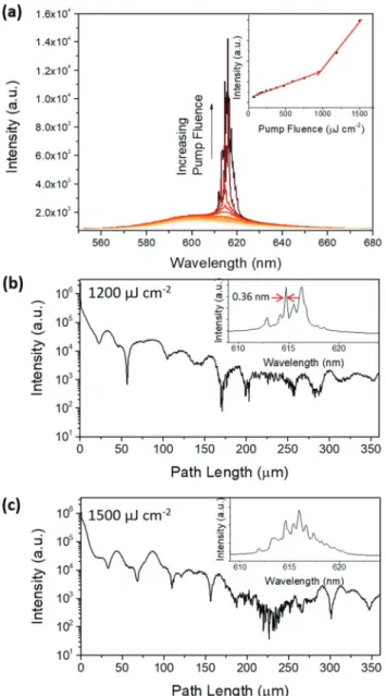
Lastly, we demonstrated the lasing from our CdSe/CdSeTe core/alloyed-crown NPLs. A scratched glass slide was used as a substrate for the dropcast NPL film with higher roughness (see AFM images in Fig. S5†). The random lasing results from the marriage of multiple scattering and optical amplification. The multiple scattering given by the micron-scale surface rough-ness provides optical feedbacks and modes, which facilitate the onset of lasing action. For practical application in lasers using colloidal NCs as gain media, the c.w. lasing is desired.46 However, it is usually difficult to achieve because the short gain lifetime resulting from the carrier losses is mainly due to fast Auger recombination. The long Auger recombination life-time in our NPLs would benefit the achievement of c.w. lasing. Notably, here we used a nanosecond Nd:YAG laser with a pulse width of 0.5 ns to optically pump the sample at 532 nm. The longer pulse duration than the Auger recombination lifetime would ensure a regime of the quasi-steady state optical gain.47,48As shown in Fig. 6a, the random lasing with multiple narrow peaks49,50was observed above a pump threshold of 950 ± 20 µJ cm−2. The lasing spectra consist of a series of spiky
Fig. 5 Characterization of ASE and Auger recombination. (a) PL emission spectra of the CdSe/CdSeTe NPLfilm under 400 nm fs laser excitation. The inset shows the integrated emission intensities as a function of the pumpfluence. (b) The emission dynamics of the ASE (black) and SE (red) above the threshold. (c) Normalized PB decay dynamics probed at CT states of CdSe/CdSeTe NPLs in solution under 400 nm excitation at different pumpfluences. The inset shows the extracted Auger-recombination dynamics. The gray lines are fittings using a bi-exponential decay function; the fitted parameters are shown in Table S3 in the ESI.† (d) PL emission spectra of the CdSe/CdSeTe film under 530 nm fs laser excitation. The inset shows the integrated emission intensities as a function of the pumpfluence.
peaks of a width of down to∼0.36 nm. In order to analyse the optical feedbacks for the random lasing, Fourier transform was performed over the random lasing spectra collected at different pump fluence levels, as shown in Fig. 6b. The path length d is the conjugate variable to the wave vector k = 2π/λ.51
The transform harmonic peak at the positions of path lengths d equals to the multiples of nL/π, where L is the cavity length and n is the effective refractive index of the optical gain medium.52As can be seen in the lasing spectra and the corres-ponding Fourier transform, the positions of lasing peaks and the resonant cavity lengths vary with pump fluence, which are
characteristics of random lasing, owing to the varied gain/loss in different optical modes or feedback paths.53,54
Conclusions
In this study, we achieved low-threshold room-temperature ASE/lasing from interfacial CT states in the colloidal type-II CdSe/CdSeTe core/alloyed crown NPLs. The type-II band align-ment is confirmed by femtosecond transient absorption and TRPL spectroscopy investigations. Our optical measurement results also revealed that the alloyed CdSe/CdSeTe interfaces have a higher PLQY and recombination rate, a higher density of CT states, a much faster carrier transfer to the interfaces and a longer Auger recombination lifetime than the type-II CdSe/CdTe NPL sharp interfaces. These merits enable the achievement of ASE with low thresholds of up to ∼60-fold lower than the threshold of ASE from CT states in type-II core/ shell quantum dots. Furthermore, the random lasing was also demonstrated in such NPL films under sub-ns laser pumping. Our findings suggest that the type-II nanoplatelets with alloyed interfaces have great potential to provide new prospects for solution-processed light emission applications such as lasers and LEDs.
Con
flicts of interest
There are no conflicts to declare.
Acknowledgements
The authors are thankful for financial support from the Singapore National Research Foundation under NRF-NRFI2016-08. The electron microscopy imaging was per-formed at the Facility for Analysis, Characterization, Testing, and Simulation (FACTS) at Nanyang Technological University, Singapore. T. C. S. also acknowledges financial support from the Ministry of Education Academic Research Fund Tier 1 grants RG101/15 and RG173/16, and Tier 2 grants MOE2015-T2-2-015 and MOE2016-T2-1-034; and from the Singapore National Research Foundation through the Competitive Research Program NRF-CRP14-2014-03. In addition, C. D. acknowledges the NTU start-up grant (M40810482).
References
1 S. Ithurria, M. D. Tessier, B. Mahler, R. P. S. M. Lobo, B. Dubertret and A. L. Efros, Nat. Mater., 2011, 10, 936–941. 2 Z. Chen, B. Nadal, B. Mahler, H. Aubin and B. Dubertret,
Adv. Funct. Mater., 2014, 24, 295–302.
3 C. She, I. Fedin, D. S. Dolzhnikov, P. D. Dahlberg, G. S. Engel, R. D. Schaller and D. V. Talapin, ACS Nano, 2015, 9, 9475–9485.
Fig. 6 (a) Random lasing from the CdSe/CdSeTe core/crown NPLfilm on a scratched glass slide excited with a sub-nanosecond Nd:YAG laser with a pulse width of 0.5 ns and 60 kHz repetition rate at 532 nm. Inset: The power transfer function of the random lasing action. (b) Fourier transform of the random lasing spectrum at afluence of 1200 μJ cm−2 (upper panel) and 1500μJ cm−2(lower panel). The corresponding lasing spectrum is given in the inset.
4 B. Guzelturk, Y. Kelestemur, M. Olutas, S. Delikanli and H. V. Demir, ACS Nano, 2014, 8, 6599–6605.
5 C. She, I. Fedin, D. S. Dolzhnikov, A. Demortière, R. D. Schaller, M. Pelton and D. V. Talapin, Nano Lett., 2014, 14, 2772–2777.
6 E. Lhuillier, A. Robin, S. Ithurria, H. Aubin and B. Dubertret, Nano Lett., 2014, 14, 2715–2719.
7 E. Lhuillier, S. Pedetti, S. Ithurria, H. Heuclin, B. Nadal, A. Robin, G. Patriarche, N. Lequeux and B. Dubertret, ACS Nano, 2014, 8, 3813–3820.
8 A. Naeem, F. Masia, S. Christodoulou, I. Moreels, P. Borri and W. Langbein, Phys. Rev. B: Condens. Matter Mater. Phys., 2015, 91, 121302.
9 L. C. Flatten, S. Christodoulou, R. K. Patel, A. Buccheri, D. M. Coles, B. P. Reid, R. A. Taylor, I. Moreels and J. M. Smith, Nano Lett., 2016, 16, 7137–7141.
10 J. Q. Grim, S. Christodoulou, F. Di Stasio, R. Krahne, R. Cingolani, L. Manna and I. Moreels, Nat. Nanotechnol., 2014, 9, 891–895.
11 Z. Yang, M. Pelton, I. Fedin, D. V. Talapin and E. Waks, Nat. Commun., 2017, 8, 143.
12 M. Li, M. Zhi, H. Zhu, W.-Y. Wu, Q.-H. Xu, M. H. Jhon and Y. Chan, Nat. Commun., 2015, 6, 8513.
13 S. Pedetti, S. Ithurria, H. Heuclin, G. Patriarche and B. Dubertret, J. Am. Chem. Soc., 2014, 136, 16430–16438. 14 S. Kim, B. Fisher, H.-J. Eisler and M. Bawendi, J. Am. Chem.
Soc., 2003, 125, 11466–11467.
15 Y. Kelestemur, B. Guzelturk, O. Erdem, M. Olutas, T. Erdem, C. F. Usanmaz, K. Gungor and H. V. Demir, J. Phys. Chem. C, 2017, 121, 4650–4658.
16 F. Fan, P. Kanjanaboos, M. Saravanapavanantham, E. Beauregard, G. Ingram, E. Yassitepe, M. M. Adachi, O. Voznyy, A. K. Johnston, G. Walters, G.-H. Kim, Z.-H. Lu and E. H. Sargent, Nano Lett., 2015, 15, 4611–4615.
17 S. A. Ivanov, A. Piryatinski, J. Nanda, S. Tretiak, K. R. Zavadil, W. O. Wallace, D. Werder and V. I. Klimov, J. Am. Chem. Soc., 2007, 129, 11708–11719.
18 A. M. Dennis, B. D. Mangum, A. Piryatinski, Y.-S. Park, D. C. Hannah, J. L. Casson, D. J. Williams, R. D. Schaller, H. Htoon and J. A. Hollingsworth, Nano Lett., 2012, 12, 5545–5551.
19 V. I. Klimov, S. A. Ivanov, J. Nanda, M. Achermann, I. Bezel, J. A. McGuire and A. Piryatinski, Nature, 2007, 447, 441– 446.
20 M. D. Tessier, P. Spinicelli, D. Dupont, G. Patriarche, S. Ithurria and B. Dubertret, Nano Lett., 2014, 14, 207–213. 21 S. Pedetti, B. Nadal, E. Lhuillier, B. Mahler, C. Bouet,
B. Abécassis, X. Xu and B. Dubertret, Chem. Mater., 2013, 25, 2455–2462.
22 B. Guzelturk, Y. Kelestemur, M. Olutas, Q. Li, T. Lian and H. V. Demir, J. Phys. Chem. Lett., 2017, 8, 5317–5324. 23 D. Gachet, A. Avidan, I. Pinkas and D. Oron, Nano Lett.,
2010, 10, 164–170.
24 Q. Zeng, X. Kong, Y. Sun, Y. Zhang, L. Tu, J. Zhao and H. Zhang, J. Phys. Chem. C, 2008, 112, 8587–8593.
25 F. García-Santamaría, S. Brovelli, R. Viswanatha, J. A. Hollingsworth, H. Htoon, S. A. Crooker and V. I. Klimov, Nano Lett., 2011, 11, 687–693.
26 C. de Mello Donegá, Phys. Rev. B: Condens. Matter Mater. Phys., 2010, 81, 165303.
27 P. V. Kamat, N. M. Dimitrijevic and A. J. Nozik, J. Phys. Chem., 1989, 93, 2873–2875.
28 X. Liu, Q. Zhang, J. N. Yip, Q. Xiong and T. C. Sum, Nano Lett., 2013, 13, 5336–5343.
29 W.-Y. Wu, M. Li, J. Lian, X. Wu, E. K. L. Yeow, M. H. Jhon and Y. Chan, ACS Nano, 2014, 8, 9349–9357.
30 C. H. Wang, T. T. Chen, K. W. Tan, Y. F. Chen, C. T. Cheng and P. T. Chou, J. Appl. Phys., 2006, 99, 123521.
31 G. Morello, A. Fiore, R. Mastria, A. Falqui, A. Genovese, A. Cretì, M. Lomascolo, I. R. Franchini, L. Manna, F. Della Sala, R. Cingolani and M. De Giorgi, J. Phys. Chem. C, 2011, 115, 18094–18104.
32 N. N. Ledentsov, J. Böhrer, M. Beer, F. Heinrichsdorff, M. Grundmann, D. Bimberg, S. V. Ivanov, B. Y. Meltser, S. V. Shaposhnikov, I. N. Yassievich, N. N. Faleev, P. S. Kop’ev and Z. I. Alferov, Phys. Rev. B: Condens. Matter Mater. Phys., 1995, 52, 14058–14066.
33 J. He, C. J. Reyner, B. L. Liang, K. Nunna, D. L. Huffaker, N. Pavarelli, K. Gradkowski, T. J. Ochalski, G. Huyet, V. G. Dorogan, Y. I. Mazur and G. J. Salamo, Nano Lett., 2010, 10, 3052–3056.
34 K. Wu, Q. Li, Y. Jia, J. R. McBride, Z.-X. Xie and T. Lian, ACS Nano, 2015, 9, 961–968.
35 S. Kaniyankandy, S. Rawalekar and H. N. Ghosh, J. Mater. Chem. C, 2013, 1, 2755–2763.
36 E. Cassette, S. Pedetti, B. Mahler, S. Ithurria, B. Dubertret and G. D. Scholes, Phys. Chem. Chem. Phys., 2017, 19, 8373– 8379.
37 I. D. W. Samuel, E. B. Namdas and G. A. Turnbull, Nat. Photonics, 2009, 3, 546–549.
38 Q. Li, Z. Xu, J. R. McBride and T. Lian, ACS Nano, 2017, 11, 2545–2553.
39 V. I. Klimov, A. A. Mikhailovsky, D. W. McBranch, C. A. Leatherdale and M. G. Bawendi, Science, 2000, 287, 1011–1013.
40 W. K. Bae, L. A. Padilha, Y.-S. Park, H. McDaniel, I. Robel, J. M. Pietryga and V. I. Klimov, ACS Nano, 2013, 7, 3411– 3419.
41 W. K. Bae, Y.-S. Park, J. Lim, D. Lee, L. A. Padilha, H. McDaniel, I. Robel, C. Lee, J. M. Pietryga and V. I. Klimov, Nat. Commun., 2013, 4, 2661.
42 R. R. Cooney, S. L. Sewall, D. M. Sagar and P. Kambhampati, Phys. Rev. Lett., 2009, 102, 127404. 43 S. L. Sewall, R. R. Cooney, E. A. Dias, P. Tyagi and
P. Kambhampati, Phys. Rev. B: Condens. Matter Mater. Phys., 2011, 84, 235304.
44 R. R. Cooney, S. L. Sewall, D. M. Sagar and P. Kambhampati, J. Chem. Phys., 2009, 131, 164706. 45 Y. Gao, G. Yu, Y. Wang, C. Dang, T. C. Sum, H. Sun and
H. V. Demir, J. Phys. Chem. Lett., 2016, 7, 2772–2778.
46 F. Fan, O. Voznyy, R. P. Sabatini, K. T. Bicanic, M. M. Adachi, J. R. McBride, K. R. Reid, Y.-S. Park, X. Li, A. Jain, R. Quintero-Bermudez, M. Saravanapavanantham, M. Liu, M. Korkusinski, P. Hawrylak, V. I. Klimov, S. J. Rosenthal, S. Hoogland and E. H. Sargent, Nature, 2017, 544, 75–79.
47 M. M. Adachi, F. Fan, D. P. Sellan, S. Hoogland, O. Voznyy, A. J. Houtepen, K. D. Parrish, P. Kanjanaboos, J. A. Malen and E. H. Sargent, Nat. Commun., 2015, 6, 8694.
48 C. Dang, J. Lee, C. Breen, J. S. Steckel, S. Coe-Sullivan and A. Nurmikko, Nat. Nanotechnol., 2012, 7, 335–339.
49 N. M. Lawandy, Nat. Phys., 2010, 6, 246–248.
50 A. Tulek, R. C. Polson and Z. V. Vardeny, Nat. Phys., 2010, 6, 303–310.
51 R. C. Polson, G. Levina and Z. V. Vardeny, Appl. Phys. Lett., 2000, 76, 3858–3860.
52 D. Hofstetter and R. L. Thornton, Appl. Phys. Lett., 1998, 72, 404–406.
53 Y.-S. Park, W. K. Bae, T. Baker, J. Lim and V. I. Klimov, Nano Lett., 2015, 15, 7319–7328.
54 H. Cao, Y. G. Zhao, S. T. Ho, E. W. Seelig, Q. H. Wang and R. P. H. Chang, Phys. Rev. Lett., 1999, 82, 2278–2281.