Modulation in InAs Quantum Dot Waveguides
B. Imran Akca1, Aykutlu Dana2, Atilla Aydinli2,Marco Rossetti3, Lianhe Li3, Andrea Fiore3, N. Dagli4Material Science and Nanotechnology Program, Bilkent University, Ankara, Turkey1 Physics Department, Bilkent University, Ankara, Turkey2
Institute of Quantum Electronics and Photonics, Ecole Polytechnique Fédérale de Lausanne EPFL, CH-1015 Lausanne, Switzerland3
ECE Department, University of California at Santa Barbara, California, USA4 1[email protected]
Abstract: Modulation in molecular beam epitaxy grown self-assembled InAs quantum dot waveguides have been studied at 1500 nm as a function of wavelength and voltage. Enhanced electro-optic coefficients compared to bulk GaAs were observed.
©2007 Optical Society of America
OCIS codes: (230.4110) Modulators; (250.7360) Waveguide modulators
Nonlinear optical and linear electro-optic materials find use as switching and modulation devices in photonic integrated circuits. Quantum dots and quantum wells have recently attracted much attention due to their enhanced electro-optic effects. Low dimensional quantum confined structures are expected to significantly enhance the performance of various optoelectronic components. [1] In this regard, we study optical transmission through multilayer InAs quantum dot lasers to investigate the degree of enhancement in electro-optic coefficient. We worked on two different types of quantum dot structures, with three (3QDs) and five layers (5QDs) of quantum dots. The waveguides with 3QDs are in the lengths of 1, 1.3, 1.6 mm and the 5QDs waveguides are 1 and 2.3 mm. The samples are grown by molecular beam epitaxy. The active region is formed by three or five layers of self-assembled InAs QDs, which are covered by a 5-nm In0.15 Ga0.85As QW and separated from each other by a
40-nm GaAs spacer layer. The areal dot density of our lens-shaped QDs is 3x1010cm-2. The active region is clad by 1.5 µm of Al0.7Ga0.3 As, which is n-doped on the substrate side and p-doped on the top side. Our devices also work as
ridge-waveguide lasers with 8 and 15 µm widths. Both facets are as cleaved. For each sample lasing is peaked at nearly 1285nm [2].
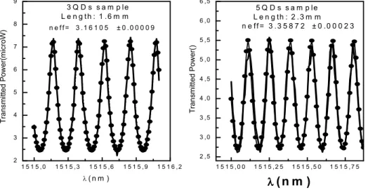
Measurement of the electro-optic coefficientsaway from EL emission peak was carried out by coupling 1.5 µm light from a tunable laser (Santec Tunable LD Light Source TSL-520)onto one end of the waveguide with a lens shaped fiber. A controlled DC voltage source was used to apply 0 to 6 Volts reverse bias to the samples. At each voltage level, the transmission through the device is recorded as a function of wavelength. The index of refraction can then be inferred from the Fabry-Perot cavity response. The experimental results and their optimum curve fits are given in Fig. 1 and 2.
1 5 1 5 , 0 1 5 1 5 , 3 1 5 1 5 ,6 1 5 1 5 , 9 1 5 1 6 , 2 2 3 4 5 6 7 8 9 1 5 1 5 , 0 0 1 5 1 5 , 2 5 1 5 1 5 , 5 0 1 5 1 5 , 7 5 2 ,5 3 ,0 3 ,5 4 ,0 4 ,5 5 ,0 5 ,5 6 ,0 6 ,5 T ra n s m it te d P o w e r( m ic ro W ) λ( n m ) n e f f = 3 . 1 6 1 0 5 ± 0 . 0 0 0 0 9 3 Q D s s a m p l e L e n g t h : 1 . 6 m m T ra n s m it te d P o w e r( ) λ λ λ λ
( n m )
5 Q D s s a m p l e L e n g th : 2 . 3 m m n e f f = 3 . 3 5 8 7 2 ± 0 . 0 0 0 2 3Figure 1. (a) The transmission power versus wavelength of the 5QDs sample. The circular dots show the optimum curve fit and the other curve is the representation of the experimental data at zero volt. (b) Same graphs for 3QDs sample.
a201_1.pdf
IWE4.pdf
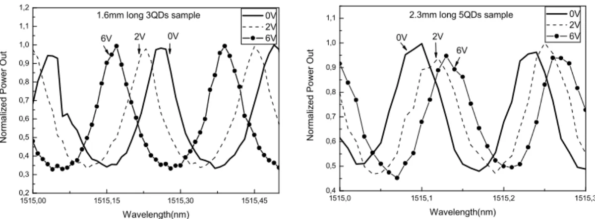
Figure 2. Transmission of the Fabry-Perot modulator as a function of the wavelength for 3QDs and 5QDs structures. Significant tuning is observed with relatively low voltages.
The linear electro-optic coefficients are obtained by fitting the measured data to the equation of transmission through a Fabry Perot modulator [3] and calculating the refractive index difference between two specific voltages. The change in refractive index due to applied voltage is ∆n V
( )
is given as [3]( )
3 41 1 2 e V n V n r t ∆ = Γwhere r is the electro-optic coefficient , 41 t is the thickness of the epilayer (t=135nm for 3QDs sample and t=225nm for 5QDs sample), neis the effective index, V is the voltage difference between two curves and confinement factor
Γ is the overlap of the vertical electric field component with the optical mode. To obtain r41, Γ needs to be known
precisely. It is clear that the confinement factor is a combination of the individual confinement factors of each material in the active region of the waveguide. Each layer contributes a different amount to the mode confinement, roughly proportional to their thickness, and quantum dot layers have the lowest confinement factor compared to GaAs and InGaAs layers due to their small fill factor in the active region. For mode shape calculations, the effect of the quantum dots on confinement due to bulk refractive index difference is neglected; we only considered the contributions of the other layers. This approximation ensures that a conservative estimate of the electro-optic coefficient is made. We, therefore present r41 normalized to Γ. The results of the measurements are given in Table 1.
Table1. Measurement results for 3QDs and 5QDs samples. Type of sample Refractive index (Voltage dependent) r41/Γ (x10-13 m/V ) 0V 2V 6V 3QDs -1.6mm 3.16123 3.16119 3.16105 7.7 3QDs -1.3mm 3.16829 3.16866 (for 3V) 3.16858 6,8 3QDs -1mm 3.16661 3.16762 (for 3V) 3.16687 5 5QDs -2.3mm 3.35862 3.35872 3.35904 17 5QDs -1mm 3.39115 3.39728 3.39813 13
These values are considerably higher than that of the materials surrounding the QDs. As a matter of fact examination of Figure 2 reveals that full on/off modulation is possible for 1.6 mm long 3 QD sample using 6 V. This corresponds to less than 1 V-cm modulation efficiency. In other words using this modulator as the arms of a push pull driven Mach-Zehnder modulator, less than 1 V drive voltage would result for 1 cm long arms. This should be possible since the propagation loss based on the fringe visibility is less than 5 dB/cm. This is far more efficient than what can be obtained using bulk materials without the QDs.
1515,0 1515,1 1515,2 1515,3 0,4 0,5 0,6 0,7 0,8 0,9 1,0 1,1 N o rm a liz e d P o w e r O u t Wavelength(nm) 0V 2V 6V 2.3mm long 5QDs sample 2V 0V 6V 1515,00 1515,15 1515,30 1515,45 0,2 0,3 0,4 0,5 0,6 0,7 0,8 0,9 1,0 1,1 1,2 N o rm a liz e d P o w e r O u t Wavelength(nm) 0V 2V 6V 1.6mm long 3QDs sample 6V 2V 0V a201_1.pdf
IWE4.pdf
© 2007 OSA/IPNRA 2007In conclusion, we have observed the low voltage modulation in InAs quantum dot waveguıdes. We have obtained the electro-optic coefficients for several waveguides with different lengths and layers of InAs quantum dots. Electro-optic coefficients as large as 7.7x10⁻¹³/Γ (m/V) for 3QDs samples and 17.0x10⁻¹³/Γ (m/V) for the 5QDs samples were obtained. This is an enhancement in both cases compared to the bulk GaAs [1].
Acknowledgement: This project is supported by TUBITAK; Grant No: 103T115. References:
[1]. L. Davis, K. Ko, W. Li, H.Sun, Y. Lam, T. Brock, S. Pang, and P. Bhattacharya, "Photoluminescence and electro-optic properties (25-35 nm diameter) quantum boxes", Appl. Phys. Lett., vol. 62, No.22, May 1993
[2]. A. Markus, J. X. Chen, C. Paranthoen, and A. Fiore," Simultaneous two-state lasing in quantum-dot lasers," Applied Physics Letter, vol. 82, No. 12, March 2003.
[3]. S. Nishimura, H. Inoue, H. Sano, and K. Ishida "Electrooptic Effects in an InGaAs/InAlAs Multiquantum Well Structure," IEEE Photonics Technology Letters, vol. 4, No. 10, October 1992.
[4]. Yariv and P. Yeh, "OpticaI Waves in Crystals", (Wiley, New York, 1984).
a201_1.pdf