CHALCOGENIDE
MICRO AND NANOSTRUCTURES
AND
APPLICATIONS
A DISSERTATION
SUBMITTED TO THE DEPARTMENT OF PHYSICS
AND THE GRADUATE SCHOOL OF ENGINEERING AND SCIENCE OF BILKENT UNIVERSITY
IN PARTIAL FULFILLMENT OF THE REQUIREMENTS FOR THE DEGREE OF
DOCTOR OF PHILOSOPHY
By
Ozan Aktaş
August, 2014
I certify that I have read this thesis and that in my opinion it is fully adequate, in scope and in quality, as a thesis of the degree of Doctor of Philosophy.
………. Prof. Dr. Mehmet Bayındır (Advisor)
I certify that I have read this thesis and that in my opinion it is fully adequate, in scope and in quality, as a thesis of the degree of Doctor of Philosophy.
………. Assoc. Prof. Dr. Ceyhun Bulutay
I certify that I have read this thesis and that in my opinion it is fully adequate, in scope and in quality, as a thesis of the degree of Doctor of Philosophy.
………. Assoc. Prof. Dr. Selçuk Aktürk
I certify that I have read this thesis and that in my opinion it is fully adequate, in scope and in quality, as a thesis of the degree of Doctor of Philosophy.
………. Assist. Prof. Dr. Ali Kemal Okyay
I certify that I have read this thesis and that in my opinion it is fully adequate, in scope and in quality, as a thesis of the degree of Doctor of Philosophy.
………. Assist. Prof. Dr. Aykutlu Dana
Approved for the Graduate School of Engineering and Science:
………. Prof. Dr. Levent Onural Director of the Graduate School
ABSTRACT
CHALCOGENIDE MICRO AND NANOSTRUCTURES
AND APPLICATIONS
Ozan Aktaş Ph.D. in Physics
Supervisor: Prof. Dr. Mehmet Bayındır August, 2014
Chalcogenides, which are glasses consist of S, Se and Te elements, are promising materials for photonics as silicon for modern electronics, due to their extraordinary material properties such as high nonlinearity and wide mid-IR transparency. However, the biggest barrier before their full extend technological exploitation is the difficulty in utilization of these unique material properties within photonic devices with various forms of desired geometries including nanowires, microspheres, and microdisks as necessitated by unique optical functionalities for specific applications, some of which are optical microresonators, modulators, and photodetection devices.
In this study, the author explore new routes for the fabrication of on-chip photonic elements with chalcogenides and consider a low cost high-yield production method with a compatible and extendable integration phase. The study illustrates production of chalcogenide optical cavities embedded in a polymer fiber, on-chip integration of the cavities having spherical, spheroidal, and ellipsoidal boundaries, and results of their optical characterizations. Besides the fabrication of active photonic devices with electro-optical capabilities, tapered chalcogenide fibers are also considered as evanescent couplers for the resonators of high index materials.
In addition, a large area chalcogenide nanowire based photodetection device is demonstrated including fabrication of photoconductive pixels, design of an electronic readout circuit, development of a custom software for a pattern detection application.
Keywords: Chalcogenides glasses, nanowires, optical microresonators, asymmetric
resonant cavities, electro-optical Kerr effect, modulators, whispering gallery mode resonators, photonics, fiber drawing.
ÖZET
KALKOJEN MİKRO VE NANOYAPILAR
VE UYGULAMALARI
Ozan Aktaş Fizik, Doktora
Tez Yöneticisi: Prof. Dr. Mehmet Bayındır Ağustos, 2014
S, Se ve Te elementlerinin bileşiminde yer aldığı camlardan olan kalkojenler, yüksek doğrusal olmayan kırılma indisleri ve geniş orta-enfraruj geçirgenliği gibi sıra dışı malzeme özellikleri sayesinde, silikonun modern elektronikte oynadığı rol gibi fotonik için gelecek vadeden malzemelerdir. Fakat ileri teknolojik kullanımlarının önündeki en büyük engel, bu malzeme özelliklerinin fotonik aygıtlarda mikrotel, mikroküre veya mikrodisk gibi özel uygulamalar için eşsiz optik işlevselliklerin gerektirdiği biçimlerde kullanılmasındaki zorluklardır. Optik resonatörler, modülatörler ve ışık algılama aygıtları bu uygulamaların bazılarıdır.
Bu çalışmada, yazar kalkojen tabanlı bütünleşmiş fotonik elemanların üretimi konusunda yeni yollar arayışındadır ve bu yolda diğer teknolojiler ile uyumlu ve genişletilebilir bütünleşme aşamaları olan düşük maliyetli çok verimli bir üretim yöntemini ele almaktadır. Çalışma, kalkojen optik kavitelerin bir polimer fiber içerisinde üretimlerinden devre üzerine küresel, küremsi ve elipsoidal şekillerde bütünleştirilmesine ve optik özelliklerin değerlendirilmesi kadar yapılanları göstermektedir. Elektro-optiksel özellikleri olan aktif fotonik elemanların üretiminin yanında bir de yüksek kırılma katsayılı resonatörlere ışık eşlemek için inceltilmiş kalkojen fiberlerin üretilmesini ele almaktadır.
Bunlara ilaveten, geniş alanlı kalkojen nano tel tabanlı bir ışık algılama aygıtının gösterimi yapılmıştır. Bu gösterim fotoiletken algılama hücrelerinin fabrikasyonunu, okuyucu elektronik devre tasarımını ve bir şekil algılama uygulaması için geliştirilen özel amaçlı yazılımı içermektedir.
Acknowledgement
First and foremost I would like to thank my academic advisor, Prof. Mehmet Bayındır, not only for the support and guidance he has provided me throughout my dissertation, but also for motivation and understanding he provided during the course of my Ph.D., enabling me to fulfill my full potential in succeeding this thesis. I always admire him and see him as an idol for an academic career.
I would like to thank, in particular, my team mates Erol Özgür, Ersin Hüseyinoğlu, and Pelin Toren not only for their technical support but also kind friendship. We together overcame too many difficulties regarding technical or scientific problems we faced. I am very lucky to have friends like them in my life time. Without them nothing would be as enjoyable as it is.
I also particularly thank another dear friend, Mehmet Kanık. I enjoyed sleepless nights we spent in lab and his cheerful conversations.
I like to study with smart and dedicated people. Being a member of Bayındır Research Group gave me that chance with an unforgivable experience, thanks to the Bayındır Research Group members. I want to express my gratitudes to: Adem Yıldırım, Bihter Dağlar, Emre Öztürk, Muhammad Yunusa, Tamer Doğan, Urandelger Tuvshindorj, Tural Khudiyev, Bekir Turedi, Pınar Beyazkılıc, Girayhan Say, Gökçen Birlik Demirel, Osama Tobail, Mostafa M. El-Ashry, İbrahim Yılmaz, Emel Gürbüz, Murat Dere, Dilara Oksüz, Hale Nur Çoloğlu, Seyit Ali Yaşar, and Nese Özgür. And also, I would like to thank all faculty members, students and engineers of UNAM-National Nanotechnology Research Center, where I feel like to be a part of a family.
And of course, I would like to thank my mother, father and little sister. Without their constant support and patience in my depressed times, nothing would be possible.
I would like to express my gratitude to The Scientific and Technological Research Council of Turkey, TUBİTAK, for the Ph.D. Scholarship I have benefited throughout my Ph.D.
“Knowing is not enough; we must apply. Willing is not enough; we must do.”
Contents
ABSTRACT ... iv ÖZET ... v Acknowledgement ... vi Contents ... vii List of Figures ... xList of Tables ... xxii
Chapter 1 Introduction ... 1
1.1. The Promise of Chalcogenides ... 1
1.2. Thesis Outline ... 3
Chapter 2 Fiber Drawing As a Method for Fabricating Chalcogenide Nano and Microstructures... 5
2.1. Chalcogenide Glasses ... 5
2.2. Glass Synthesis ... 7
2.3. Thermal Fiber Drawing ... 8
2.4. Iterative Size Reduction Technique ... 9
Chapter 3 Large Area Chalcogenide Nanowire Based Photodetection Device……….11
3.1. Introduction ... 11
3.2. Fabrication and Characterization of Selenium Wires ... 12
3.3. Integration of Selenium Nanowire Arrays ... 15
Chapter 4 Whispering Gallery Mode Resonators ... 23
4.1. Introduction ... 23
4.2. Ray Optics in 3D Cavities ... 25
4.2.1. Vector Formulation of Refraction ... 25
4.2.2. Vector Formulation of Reflection ... 26
4.2.3. Ray Tracer Algorithm and Simulation Results ... 27
4.3. Electromagnetic Theory of WGMs ... 30
4.4. Numerical Simulations of WGMs ... 33
4.5. Free Spectral Range ... 36
4.6. Finesse ... 36
4.7. Mode Volume ... 37
4.8. Quality Factor ... 37
Chapter 5 Optical Coupling to WGMs ... 40
5.1. Introduction ... 40
5.2. Optical Modes of Step-Index Fiber Waveguide ... 42
5.3. Numerical Simulation of Fiber Modes ... 44
5.4. Theory of Optical Coupling for the Sphere Cavity and Fiber System ... 47
5.5. Fabrication of Tapered Optical Fibers ... 54
5.6. Optical Coupling and Cavity Characterization System ... 59
Chapter 6 A New Route for Fabricating On-Chip Chalcogenide Microcavity Resonators ... 62
6.1. Introduction ... 62
6.2. Fabrication of Chalcogenide Microcavities ... 64
6.3. On-chip Integration of Chalcogenide Microcavities ... 75
6.4. Optical, Material and Surface Characterizations ... 79
Chapter 7 Electro-Optic WGM Resonator Based Chalcogenide Photonic Devices………87
7.2. Simulation of WGMs in an Electro-optic Cavity ... 88
7.3. Fabrication of Electro-Optic Photonic Devices ... 94
Chapter 8 Tapered Chalcogenide Fibers as High Index Evanescent Optical Couplers………...100
8.1. Introduction ... 100
8.2. Tapering Chalcogenide Core Polymer Cladding Fibers ... 101
8.3. Direct Drawing of Microwires from Bulk ChGs ... 103
8.4. Tapering ChGs between Silica Fibers Tips ... 104
Chapter 9 Conclusions and Future Work ... 111
Bibliography ... 113
Appendix A Matlab Codes... 124
A.1. WGMs of Sphere Cavity Resonator... 124
List of Figures
Figure 2.1: Infrared transmission spectra for various materials including ChGs [14]. 6 Figure 2.2: Chalcogenide glass synthesis. Process consists of three steps (a) material selection, (b) material purification and sealing, (c) rocking and homogenization. ... 7 Figure 2.3: (a) Optical picture of a preform before and after thermal drawing. (b) Fiber tapering tower and basic components. (c) Chalcogenide core PES cladding fibers produced by thermal drawing... 8 Figure 2.4: Steps of iterative size reduction technique resulting into one dimensional micro and nano-structures encapsulated by polymer jacket. ... 10 Figure 2.5: (a) A chalcogenide semiconductor rod is reduced to (b, c) hundreds of meters of single 200 µm wire, (d, e) 30 wires of 5 µm diameter and (f, g) 1.000 wires of 250 nm. Nanowires are extracted from polymer matrix by dissolving the polymer encapsulation in organic solvents, retaining their global alignment. Inset: Transmission electron microscopy image of a single 32-nm-thick nanowire. ... 10 Figure 3.1: SEM image of the amorphous selenium nanowire array. ... 12 Figure 3.2: Electrical characterization setup used for the measurements of photoconductive properties of Se nanowires. ... 14 Figure 3.3: Size-dependent photoconductivity of selenium nanowires. Light was on-off modulated and meantime photocurrent was recorded at applied voltage of 10 Volts. ... 14 Figure 3.4: Macroscopic assembly of nanowires over a lithographically defined circuitry. (a) First step of nanowire integration to a macroscopic circuitry is manual alignment and accommodation of polymer fiber arrays containing hundreds of nanowires embedded inside. Second step is dissolving the polymer encapsulation and dispersion of nanowires over electrode pairs as monolayers. Third step is crystallization of the selenium nanowires with pyridine solution.(b) Optical microscope image of gold electrical pathways for signal and ground electrodes on the circuit... 15
Figure 3.5: SEM image of the photodetection circuit with nanowire based pixels. (a) SEM image of crystallized selenium nanowires lying over ground and readout electrodes of the circuitry forming pixels. (b) SEM image of a single pixel, composed of hundreds of photoconductive selenium nanowires aligned over electrode pairs, which have a separation of 10 micrometers. A high resolution SEM image of nanowires can be seen in the inset. ... 16 Figure 3.6: Electrical circuit design of nanowire based photodetection device. ... 18 Figure 3.7: Printed circuit board layout of nanowire based photodetection device. .. 18 Figure 3.8: Photodetection device with electronic hardware and selenium nanowire integrated circuitry on the top. Device can be powered by USB or external power source. Each pixel is addressed by multiplexers and sampled by microprocessor. A voltage signal corresponding to a level of light intensity is measured for every pixel and data is transferred to a PC via USB. ... 19 Figure 3.9: User interface of the developed software for the construction of captured image by the nanowire based photodetection device. ... 20 Figure 3.10: Histogram of pixel photo-sensitivities normalized with minimum level of current that can be detected by the circuit. ... 20 Figure 3.11: Demonstration of the large area nanowire based photodetection device. (a) Schematics of dark field illumination of some characters onto nanowire integrated photodetection device. (b) Software constructed image of a calibrated device after full exposure to a light source for static dark and bright illumination. (d) Captured images of dark field illuminated alphabetic characters of “UNAM”. Blue pixels are dead pixels. ... 22 Figure 4.1: a) Circulating light ray inside a high index cavity (n1 > n2) via total internal
reflection. b) Schematics of incident 𝑥 , reflected 𝑢 and refracted 𝑢′ rays at the interface. ... 25
Figure 4.2: Different ray trajectories in a toroidal cavity. (a) Whispering gallery modes. (b) Bowtie modes. (c) Spiral modes. (d) Chaotic modes. Units of axes are meter. ... 28
Figure 4.3: (a) Lumerical FDTD simulation configuration. (b) High radial order modes in an oblate ellipsoidal cavity. (c) Caustics of modes in 3D perspective. (d) Caustics of modes in top view. Units of axes are meter. ... 28 Figure 4.4: Different caustics and escaping mechanisms in a triaxial ellipsoidal cavity. (a) Outer caustics. (b) Inner caustics. Escape trajectory of a horizontal mode in a (c)
top and (d) perspective view. Escape trajectory of a skewed mode in a (e) top and (f)
perspective view. Units of axes are meter. ... 29
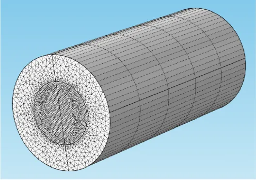
Figure 4.5: Two dimensional axisymmetric FEM based COMSOL simulation. (a) Simulation environment showing half of the sphere of radius 25 µm, air region and perfectly match layer. (b) Zoomed-in figure showing a part of the mesh. ... 33
Figure 4.6: Results of FEM simulation showing electric field distribution of Whispering Gallery Modes in a sphere of 25 µm radius. Radial mode number q is 1 for all modes and the angular mode number l takes values in 272-275. White arrows show electric field vector of WGM. ... 34
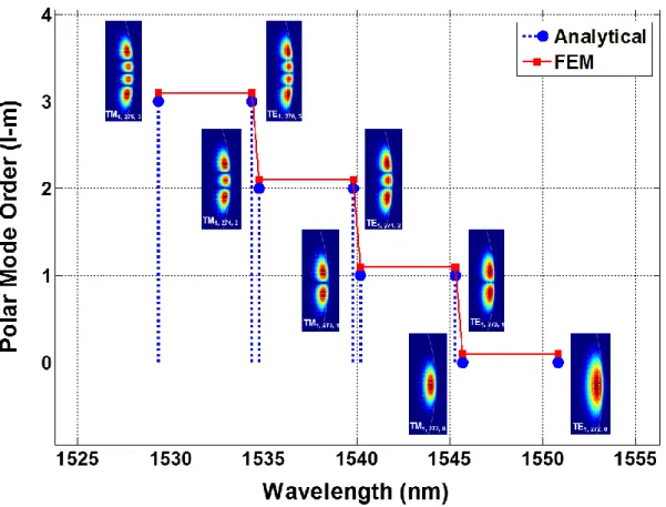
Figure 4.7: Graphics of resonance wavelengths positions calculated by FEM simulations and analytic expression of Equation 4.16. ... 35
Figure 5.1: Mesh distribution of a fiber waveguide with air cladding. Simulation parameters are : Rf = 1.8 µm, L = 15 µm, nf =1.44, λ = 1.55 µm. ... 45
Figure 5.2: Simulation result for the fundamental mode HE11 propagating along the fiber waveguide. ... 45
Figure 5.3: Electric field magnitudes and vector fields in cross section for some fiber guided modes. ... 46
Figure 5.4: (a) Cross section of the coupling region. (b) Schematic of a tapered fiber evanescently coupled to WGM of a microsphere. ... 47
Figure 5.5: The effective refractive indices neff,s of chalcogenide microspheres with various sizes for different modes of radial orders (𝑞 = 1, 2, 3 … 10), and effective refractive indices neff,f of tapered silica fiber with respect to its waist radius (for fundamental HE11 mode). Radius of the microresonator is R = 25 µm. ... 49
Figure 5.6: TE and TM WGM modes for a sphere of 25 µm radius with ns = 2.79. . 53
Figure 5.7: Fiber tapering setup used for the fabrication of tapered silica fibers. ... 55
Figure 5.8: Schematic for fiber tapering setup. ... 56
Figure 5.9: User interface of fiber tapering system software. ... 56
Figure 5.10: SEM images of a tapered fiber fabricated by the tapering setup. ... 57
Figure 5.11: Transmission through the optical fiber during fiber tapering. Transmission is given as a function of the total tapering length. Adiabatic and non-adiabatic instances of fiber tapering can recognized from transmission data showing beating of fiber multi-modes observed as oscillations. ... 57 Figure 5.12: Transmission spectra of a silica fiber before and after tapering process with good adiabaticity. Only a parasitic loss is expected for an adiabatic fiber
irrespective of the used wavelength. Otherwise, there would be a wavelength dependent transmission dips in the spectra, due to the beating of higher modes with the fundamental mode of the fiber. ... 58 Figure 5.13: Schematics of experimental setup used for the optical characterization of microresonators. ... 59 Figure 5.14: Tapered fiber coupling to a microsphere cavity resonator of 25 µm in radius. ... 60 Figure 5.15: User interface of the developed software for optical characterization of microcavities. ... 61 Figure 5.16: Two oscilloscope channels during a single wavelength scan. A linear fit to the wavelength channel is used to find start and stop wavelength points in the time axis. After calibration of both axis, data can be plotted in wavelength (nm) vs. power (W) format by the software during data acquisition. ... 61 Figure 6.1: Formation of spherical microresonators in centimeter long polymer fibers. In order to produce a long chain of uniform As2Se3 microspheres embedded in a PES
fiber, a novel method was developed, which takes the advantage of convective (non-contact) heating of fiber under a conformal cover assisting integrity and straightness of the fiber during the process. (a) A 12 centimeter long fiber was accommodated on a 10 mm diameter glass tube and (b) covered by a supporting vacuum tape (Kapton tape) which can stand high temperatures (over 320 ºC). In order to eliminate contact heating of fiber, the glass tube was isolated by two circular Teflon spacers from the walls of a custom-made tubular oven. (c) The tubular oven supplies necessary uniform heating with circular temperature distribution inducing PR instability in the fiber core. Releasing built-in stress, length of the fiber finally was reduced approximately to the half of initial length. After 15 minutes at 300 ºC, chalcogenide core polymer cladding fiber turned into a long self-assembled chain of microspheres held immobile in the cladding. After removing the cover tape and cutting uneven ends of the fiber, 5 centimeters long product, which is the longest fiber with embedded microspheres reported, was obtained at the end. ... 65 Figure 6.2: In our simulation, we used temperature dependent viscosities for both of the polymer cladding and the glass core. The As2Se3 and PES viscosities were
determined by the universal logarithmic models.[95, 96] For the PES, we performed rheometry measurements to make sure that the viscosity used in the model was realistic
Specs). The PES model consists of two parts which are Model 1 (Arrhenius) for high temperatures and Model 2 with slightly varying activation energy for low temperatures.[96] Even the first order approximation of all Arrhenius relation gives more accurate modeling of PES viscosity than assuming a constant viscosity. This is because the viscosity contrast determines not only the instability wavelength, but also the characteristic time. ... 67 Figure 6.3: Simulation and experimental snapshots showing the evolution of microsphere formation in the As2Se3 core of a PES cladding fiber by Plateau-Rayleigh
(PR) instability. (a) A finite element fluid dynamics simulation discloses clearly the dynamics of PR instability occurring in the fiber. (b) Initially intact 80 µm diameter chalcogenide core of the polymer cladding fiber turns into a self-assembled chain of 160 µm diameter spheres and smaller satellite spheres embedded inside the fiber, in 15 minutes at 300 °C. (c) A photograph of a 5 cm long PES cladding fiber with embedded As2Se3 microspheres. ... 68
Figure 6.4: Fractal process of microsphere formation by Plateau-Rayleigh instability. (a) Optical microscope pictures show fractal nature of PR instability occurring in a fiber core. Successive optical micrographs of the fiber, showing inner structure with increasing detail are taken by using 5X, 10X and 20X objectives, respectively. Although the process is self-quenching after a number of generations finally reaching submicron scales, satellite and sub-satellite sphere formation between main spheres (the first generation) can be seen down to 5th generation. Numerical simulations also reveal same fractal pattern of in-fiber sphere formation. Numbers 1-5 in the figures indicate number of sphere generations. (b) Rule of thumb is as simple as graphically represented by the figure; i.e., for every next generation, two smaller satellite spheres are supposed to reside at the sides of larger spheres of previous generation. ... 69 Figure 6.5: Theoretical comparisons of instability wavelength with experimental data. Comparison of the temperature dependent normalized (with respect to the initial core diameter d) average instability wavelength of experimentally produced micro-spheres and theoretically calculated data based on Tomotika model [91] and our 2D finite element numerical simulation. At low temperatures, the simulation coincides very well with the experiment, while Tomotika model over-estimate the instability wavelength. When the temperature is increased, both the simulation and the analytical models under-estimate the experimentally measured instability wavelengths. The best agreement between the three data sets is at moderate temperatures (T = 280-300 oC).
Therefore, we chose this range for comparing the results of experiments and simulation of sphere formation. ... 70 Figure 6.6: Characteristic time of fiber core break-up. The variation of the characteristic time () as a function of temperature T. The characteristic time is defined as the time at which the break-up starts. The logarithmic decrease of with temperature follows two different activation regions intersecting at a point, which coincides with the viscosity contrast turning point (around 310 oC as in Figure 6.2)... 71 Figure 6.7: High yield production of 3D asymmetric microresonators via continuous volume preserving transformations induced by controlled plastic deformations. (a) Schematics of fiber deformation between two parallel glass plates in a high temperature furnace. Mechanical deformation of a PES polymer fiber enclosing an As2Se3 microsphere array at a temperature above the Tg of the both materials,
transforms (b) the array of spheres into (c) an array of triaxial ellipsoids, then into (d) an array of “cigar-shaped” bodies globally oriented in perpendicular direction to the fiber axis. SEM micrographs show (e) spherical, (f) ellipsoidal and (g) “cigar-shape” cavities extracted out by dissolving the PES polymer cladding in DCM. SEM micrographs show (h) ellipsoidal and (i) “cigar-shape” resonators in profile view. . 73 Figure 6.8: Microresonator array deformation setup. Experimental setup used for deformation and integration of microresonator arrays is actually a contact angle measuring system (DataPhysics OCA30) possessing a high temperature furnace (up to 400ºC) with temperature control. The system consists of a CCD camera, a long working distance microscope and a light source for process monitoring, an electrical furnace with two hotplates on top and bottom sides, and a z axis motorized stage under the furnace and a cylindrical bar attached to a z & y axis linear stage for alignment and deformation operations. Inset shows a fiber with embedded microspheres ready to be compressed. ... 74 Figure 6.9: Conventional integration approaches: a) Microcavities attached to fibers. b) Manually arranged ellipsoidal cavities. c) Spherical cavity on a sticky tape. ... 76 Figure 6.10: High yield production and on-chip integration of chalcogenide WGM microresonators on an arbitrary substrate. (a) The process starts with fabrication of As2Se3 core PES cladding fibers by thermal drawing. Then, in-fiber microsphere
formation is induced by PR instability at elevated temperatures. As a third step, partial abrasion of the fiber cladding is achieved by a simple sandpapering process, exposing
resulting fiber is transferred manually onto a substrate spin coated with P(VDF-TrFE) polymer and then heated to promote adhesion up to a temperature of 210 °C, which is below the Tg of PES cladding; however, above the Tg of both As2Se3 core and
P(VDF-TrFE) coating. At the last step, the largest microcavities attached to the surface, can be released from the encapsulating PES polymer by selective dissolution in DCM, which has minimal effect on the substrate polymer coating. All satellite spheres are also flushed away spontaneously by the dissolution process. Optical micrographs show (b) top, side and bottom views of the fiber after sandpapering one of its sides, (c) on-chip spherical chalcogenide microresonator array, (d) spherical microresonators directly integrated on gold coated surface without any polymer coating, and (e) ellipsoidal microresonators integrated on P(VDF-TrFE) polymer coated surface. All scale bars are 100 µm. ... 77 Figure 6.11: SEM micrographs of on-chip spherical/spheroidal/ellipsoidal chalcogenide microresonator arrays. Close-ups of some individual resonators in top and profile perspectives, show quality of production and on-chip integration such as the alignment of characteristic features (like equator plane), eccentricity, smoothness, and cleanliness of the resonator surfaces. (a) Top and profile SEM micrographs of spherical As2Se3 microresonator array and a single microsphere. Average diameter of
spheres is dave = 124.4 μm with standard deviation σ = 3.4 μm (2.7%). As can be seen
in the profile of the resonator, transfer and integration of the microsphere is accomplished with a very low aspherical deformation, and a good degree of parallel alignment of the equator plane with respect to the substrate surface. Top and profile SEM micrographs of (b) a spheroidal As2Se3 microresonator array and a single
microspheroid, and (c) an ellipsoidal As2Se3 microresonator array and a single
microellipsoid. ... 78 Figure 6.12: Characterization of microresonator material composition. Energy dispersive X-ray spectroscopy (EDX) results obtained from on-chip microsphere resonators which were extracted out of their PES polymer encapsulation using DCM. EDX is attached to FEI Quanta 200 FEG SEM system. Peaks represent consistence of the atomic ratio of As2Se3. Besides, there was no impurity or residual polymer
observed on the surface of microspheres after the dissolution process. ... 80 Figure 6.13: AFM surface characterization of an ellipsoidal microresonator on (500 nm×500 nm) top polar region shows sub-nanometer rms surface roughness (σ < 0.6 nm). ... 80
Figure 6.14: Optical characterizations of on-chip spherical and spheroidal chalcogenide microresonators. (a) Transmission spectra of an As2Se3 microsphere
resonator of 50 μm in diameter. Coupling strength of resonance modes can be as high as 10 dB. FSR is 6.39 nm. (b) Lorentzian fit to a resonance dip at 1551.858 nm shows that the FWHM and loaded quality factor QL of the resonance mode are 4.9 pm and
3.1 × 10⁵ , respectively. Inset shows evanescent coupling of light into the microsphere resonator using a tapered silica fiber with a sub-micrometer waist diameter. (c) Transmission spectra of an AsSe3 microspheroid resonator of 57 μm in equator
diameter. FSR is 5.22 nm. (d) Lorentzian fit to a resonance dip at 1571.589 nm shows that FWHM and loaded quality factor QL of resonance mode are 7.2 pm and 2.2 × 10⁵,
respectively. Inset shows evanescent coupling of light into the microspheroid resonator using a tapered silica fiber... 81 Figure 6.15: Schematic of the tapered fiber coupling to WGMs of on-chip spherical cavity resonators... 81 Figure 6.16: The resonance dips in the spectra of As2Se3 microresonators were
observed to red-shift with increasing incident powers for both directions of wavelength scans. Although an un-shifted resonance dip (red), which was captured using very low optical powers with 300 pm scan range and 1 nm.s-1 scan speed, has a regular
Lorentzian shape, red-shifted versions of the resonance mode (blue, black) have characteristic “shark fin” shapes.[86] Since As2Se3 has relatively high absorption
coefficients as compared to silica in this scan range, red-shifts of modes are expected, due to the heating of the resonator via absorption of the coupled light resulting in a thermal change of the refractive index and thermal expansion of resonator diameter. Reduction in the coupling strength is another manifestation of thermo-optic effect, caused by insufficient scan speed at some power levels for which wavelength shift can be more than line width of the resonance mode at some point during wavelength scanning [99]. ... 82 Figure 6.17: Optical properties of a commercial As2Se3 glass [100] are given in terms
of (a) refractive index n and absorption α as function wavelength λ. Absorption is α = 1.6 m-1 at 1550 nm. (b) Absorption limited quality factor Q
abs can be calculated
from (n, α) data, as 𝑄abs = 2𝜋𝑛/𝜆𝛼. Qabs for As2Se3 is found to be 7.2×10⁶ for λ =
1550 nm and n = 2.83, which is an upper bound for intrinsic Q-factorsin the case of ultra-smooth and clean resonator surface. Although As2Se3 has relatively high
very promising material for microresonators in mid-IR applications, due to low absorption and high Kerr nonlinearity. ... 84 Figure 6.18: This snapshot of a movie recorded by a thermal camera, shows optical coupling to an ellipsoidal microcavity using a silica tapered fiber approaching from the bottom. Bright spot on the left in the middle is an ambient scattered light reflected from the surface, which is irrelevant to optical coupling with the tapered fiber. ... 86 Figure 7.1: (a) A two dimensional axisymmetric simulation based on FEM is used to analyze WGMs in an electro-optic chalcogenide disk cavity, which is a sphere trimmed at both polar regions. (b) Different sizes for mesh elements are used in the simulation. The densest mesh is where WGMs are located, i.e., around equatorial region. ... 89 Figure 7.2: The result of the COMSOL simulation shows a fundamental WGM in an electro-optic disk cavity resonator under an applied voltage. First electric field distribution is found, which is caused by the potential difference between the gold electrode at the top and the infinite plane gold electrode at the bottom of the cavity. The electric field modifies the refractive index of the cavity due to electro-optic Kerr effect. Therefore, Maxwell Equations were solved by using refractive index n(Eext) as
a function of external electric field. ... 89 Figure 7.3: Figure shows WGMs of different mode order (q, l, l-m) for (a) TE and (b) TM polarizations inside the disk cavity under an applied electric field. ... 91 Figure 7.4: (a) Distribution of electric field vectors between gold electrodes and a fundamental WGM exposed to different refractive indices for TE and TM modes whose electric fields are parallel and perpendicular to the cavity surface, respectively. (b) An isotropic disk cavity under an electric field behaves as an anisotropic uniaxial crystal of extraordinary 𝑛 ∥ and ordinary 𝑛 ⊥ refractive indices. ... 92 Figure 7.5: Distribution of extraordinary refractive index change ∆𝑛|| at an external voltage of 100 V. ... 92 Figure 7.6: Results of COMSOL simulation show that the relative resonance wavelength shifts have different quadratic dependence on the applied DC voltage for TE and TM polarizations. As voltage increases, WGMs split due to their different spatial mode distributions and asymmetry of the electric field inside the cavity. ... 93 Figure 7.7: Fabrication and integration steps of an electro-optic photonic device based on chalcogenide WGM disk cavity. Process starts with a chalcogenide core polymer cladding fiber and ends with an electro-optic photonic device consists of WGM disk cavity resonator between two integrated electrodes... 95
Figure 7.8: Optical microscope images of the disk cavities (a) before and (b) after PES polymer encapsulation is removed by DCM. (c) Close-up image of a single cavity from ... 96 Figure 7.9: (a) SEM micrographs of (a) a disk cavity resonator array and (b) a single disk cavity from top and side views. ... 96 Figure 7.10: Fabrication and integration process of chalcogenide disk cavities on a gold coated substrate. (a) Process starts with a fiber encapsulating sphere cavities. (b) Lower side of the fiber is removed by a sandpapering process and then (c) attached onto a gold coated substrate by heating and pressing at a temperature of 260 °C in a hot oven. (d) Second sandpapering operation on the upper surface of the integrated fiber. (e) 5 nm Cr and 15 nm gold sputtering on the upper surface of the integrated fiber for lift-off process. ... 97 Figure 7.11: Optical microscope images show a metal coated fiber encapsulating disk cavities (a) before and (b) after the dissolution of polymer by organic solvents resulting into an unsuccessful lift of process. ... 98 Figure 7.12: (a) Optical microscope image shows surface of a fiber with embedded disk cavities after the lift-off process. Sequential images show a top surface of a disk cavity after (b) O2 plasma etch, (c) gold metal sputtering and (d) lift-off process by
THF. ... 99 Figure 7.13: SEM micrographs of a disk cavity with a gold coating on the top surface from a (a) perspective and (b) side view. ... 99 Figure 8.1: (a) Custom made electrical heater with side opening for entrance and exit of the fiber, and observation during tapering process. (b) Set up used for tapering chalcogenides. (c) Close-up picture of tapered chalcogenide core PES cladding fiber. ... 101 Figure 8.2: Formation of cylindrical chunks of matter inside the tapered region due to low temperature and tensile stress caused by tapering... 102 Figure 8.3: (a) Tapering of Step 1 chalcogenide fiber with thermoplastic polymer having one side contact with inner surface of heater, results in good tapering, but only for one side. (b) Tapering of a single core chalcogenide fiber (Step 2) with a thicker cladding and a free standing chalcogenide wire after removal of PES encapsulation by organic solvents. ... 102
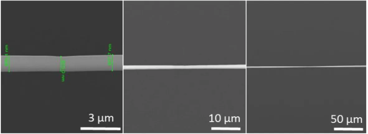
Figure 8.4: (a) Chalcogenide microwires can be easily directly drawn from bulk glass inside an oven at 260 °C being attached to a tip of cleaved silica fiber. (b) Tip of tapered wires is of order of 1 micron. ... 103 Figure 8.5: Production of microwires on the tip of a tapered silica fiber by direct drawing from bulk glass with steps of (a) approach and (b) retraction. (c) Chalcogenide tapered wire on the tip of a silica fiber tip shows super elastic properties... 104 Figure 8.6: Schematic of tapering chalcogenide fibers between silica tapered fiber tips with five basic steps: 1. Tapering and cleaving silica fiber, 2. Attaching some amount of chalcogenide glass on the cleaved tips inside heater one by one, 3. Alignment of silica fibers inside the electrical heater, 4. Moving silica fiber closer and merging chalcogenide glasses between two fiber tips. 5. Tapering suspended material by drawing silica fibers away. ... 105 Figure 8.7: Cleaving tapered silica fibers. (a) Side view and (b) down view of cleaving process with a sharp blade. Scoring surface of fiber is enough to cleave tapered fibers under tensile stress. ... 106 Figure 8.8: Cleaved tips of (a) tapered and (b) normal fiber before attachment of chalcogenide glass. ... 106 Figure 8.9: Two different ways of attaching chalcogenide glass on silica fiber tips can be realized a) in temperature controlled oven or b) inside the electrical heater, which is advantageous since there is no need to move tapered silica fibers already connected to laser source and power meter at the silica fiber tapering process. ... 107 Figure 8.10: (a) Evolution of chalcogenide tapering process starts with two silica fibers with some chalcogenide glass on them and results into tapered chalcogenide fiber between two silica tips being apart. (b) Optical microscope image of intentionally broken tapered chalcogenide fiber spliced to a silica tapered fiber ... 108 Figure 8.11: Steps of tapering chalcogenide between cleaved silica fiber tips. (a) Tapering and cleaving silica fibers. (b) Attaching chalcogenide glass by inserting silica tips into bulk chalcogenide glass. (c) Alignment of silica fiber tips inside the electrical heater. (d) Merging chalcogenide glasses between both tips moving closer to each other. (e) Initial stretch of the merged chalcogenide glass to ensure correct working temperature. (f) Stretching suspended chalcogenide glass which transforms into tapered fiber between silica tips being apart. (g) SEM micrograph of the produced chalcogenide fiber between silica tips showing smooth junction points and tapered region of 2 µm radius. ... 109
Figure 8.12: Transmission spectra of tapered silica fiber before in-situ cleaving (upper line) and of chalcogenide tapered fiber suspended between two tapered silica fibers (lower line). Large dips of transmission signal is caused by the interference of beating multi-modes. ... 110
List of Tables
Table 4.1: Comparison of FEM simulation and analytic results. Resonance wavelengths are given in the unit of nanometer... 35 Table 5.1: Comparison of FEM and exact results for propagation constants of some modes. ... 46 Table 5.2: Simulation parameters for the calculation of WGM modes. Qin =105 is taken
Chapter 1
Introduction
1.1. The Promise of Chalcogenides
Silicon is the workhorse of the electronics industry which have amazingly transformed the life we live in. Thanks to this special material, today our global world is more connected than ever after the advent of the internet, cell phones, and relevant electronic applications. However, ever increasing needs to store, manipulate and transfer enormous amount of daily produced data, demands new solutions that can overcome the fundamental limitations of silicon and electronics. Solutions generally require a paradigm shift in the selection of materials and methodologies for handling information. Theoretically, chalcogenides are promising materials possessing the potential to fulfill all the needs and requirements due to their unique material properties, and photonics with integrated chalcogenide elements capable of electro-optical and all-electro-optical effects at same time is expected to transform the future the way electronics did.
Chalcogenides, which are amorphous semiconductors containing chalcogen elements of Se, S, and Te, have already been exploited in various applications including solar cells [1], sensors [2], electronics [3], and photonics [4]. Optical data storage based on chalcogenides have been very beneficial in memory applications [5], and recently, chalcogenide phase change memory technology [6] have been attracted huge interest for the fabrication of the ideal memory of the future, which is ultrafast, nonvolatile, scalable, low cost, and has very low power operation and long life cycle.
modulated to carry meaningful information. Photonic integrated circuits (PIC) can modulate light at data rates well beyond the capability of electronics (> 1 Tb/s) using all optical means [7, 8] which can benefit from optical properties of chalcogenides such as ultra-fast high Kerr nonlinearity, low two photon absorption and wide IR transparency [9]. Combining all-optical and electro-optical properties in resonant cavities can be the ultimate solution for ever increasing needs of communication, and interfacing with electronics can be obtained without causing any bottlenecks.
In addition, chalcogenides have been used as host media for laser applications since they have low phonon energy and can be doped by rare earth elements [10]. Nonlinear optical applications have also exploited chalcogenides in applications such as generation of supercontinuum [11] and Raman lasing [12].
Developing new methods for material synthesis and harnessing this special material properties in the form of specific geometries such as nanowires and microwires for fabrication of phase change memories and photodetectors, and microsphere and microdisks for photonic applications, are the current field of intense research still waiting some answers for the problems hindering ultimate utilizations of chalcogenides.
This thesis is devoted to developing new strategies and concepts enabling chalcogenides to be utilized in novel photonic applications. Starting with chalcogenide fiber drawing for the production of micro and nano structures, we used chalcogenide fibers as a versatile media to produce functional structures in different forms including wires, spheres, spheroids, ellipsoids, disks and tapers for photonic applications.
Chalcogenide nanowires were produced by a new fabrication method we recently reported. Integration of selenium fibers on a very large scale electrical circuits was achieved, and nanowire based photodetection device was demonstrated as an application.
Chalcogenide resonators have been drawn an increasing interest for nonlinear optical applications. However, duality between production and integration phase of these resonators have been hold back the applications so far. What resolved in this thesis is finding a way out of this dilemma, hence paving the way for a myriad applications for photonics. Chalcogenides have been generally used for their all optical properties in photonic applications, but their quadratic electro-optical properties is somehow ignored up to now. Therefore, we also focus on building electro-optical resonator based chalcogenide photonic devices in this thesis.
There have been an enormous need for high index evanescent couplers to couple light efficiently into high index material resonators. Although recent studies have made some progress for the fabrication of tapers from high index fibers, still some problems are waiting to be addressed such as splicing to silica fibers or mechanical instabilities. We believe that we have resolved all these issues after developing an approach for the fabrication and interfacing of the chalcogenide fibers.
1.2. Thesis Outline
The contents of this thesis are organized in a historical sequence, which was followed by the author during lifetime of this research adventure. Contents of individual chapters are given and any collaboration with other members of Bayıdır Group is stated explicitly.
Chapter 2 is an introductory chapter giving information about chalcogenides, basic methodology used in the material synthesis, fundamentals of fiber drawing, and importance of iterative size reduction technique as a new nanotechnology tool for the fabrication of nano and microstructures.
Chapter 3 demonstrates design and application of a device, which is the first of its kind, a large are nanowire based photodetection circuitry. Production of selenium fibers using iterative size reduction technique were done by Mehmet Kanık and Dr. Mecit Yaman. Integration of nanowires and optical characterizations were done in collaboration with Erol Özgür.
Chapter 4 gives a theoretical background for Whispering Gallery Modes resonators. Simulations results illustrate WGMs in sphere microcavities.
Chapter 5 gives theoretical background for evanescent coupling to optical resonators, and information about fabrication of tapered fiber couplers. Experimental setup used for optical measurements are also presented to give a complete picture for optical coupling and characterization of the resonators before the subject is mentioned in relevant chapters.
Chapter 6 explains a new method developed for the production and integration of chalcogenides cavities, which is expected to give a momentum in this field. Optical, material and surface characterizations of the produced cavities are also considered. COMSOL simulations of in-fiber microsphere formation based on Plateau-Rayleigh instability were done in collaboration with Dr. Osama Tobail.
Chapter 7 shows a new direction for the production of active chalcogenide cavities with emphasis on their electro-optical capabilities. A FEM based simulation of WGMs in an electro-optic cavity is illustrated, and production steps towards realization of on-chip active chalcogenide disk cavities are discussed with ups and downs of experimental approach.
Chapter 8 discusses three different approaches for the tapering of chalcogenides, and finally represents an ideal solution to the problem, which is of paramount importance for the achievement of efficient optical coupling into cavities of high index material.
Chapter 9 summarizes what have been done through the thesis and gives a quick glimpse for future directions.
Appendix A gives MATLAB codes used for some calculations and simulations used in Chapter 4 and Chapter 5.
Chapter 2
Fiber Drawing As a Method for
Fabricating Chalcogenide Nano and
Microstructures
2.1. Chalcogenide Glasses
Chalcogenide glasses (ChGs) are important amorphous semiconductors containing at least one of chalcogen elements (sulphur, selenium and tellurium) from group 6A of periodic table, which are covalently bonded to glass formers such as As, Ge, Ga, and P. Due to the large composition space enabling optimization of material properties as demanded by specific applications, chalcogenide have been utilized in a broad range of technology and research areas such as photonics [4], phase change memory [6] and sensors [2].
ChGs have low phonon energies due to the covalently bonded heavy atoms with low vibrational energies, making them good hosts for rare earth dopants such as Nd3+
and Er3+ [10]. Therefore, they have lower softening temperatures and hardness, and
higher thermal expansion coefficients [13]. However, their long wavelength cut-off lies in the mid-IR region [14], making their transparency in the range of 1.5-20 µm as shown in Figure 2.1. In addition, they have high refractive indices (n = 2.2-3.4) and nonlinear refractive indices n2 two or three orders of magnitude higher than that of
silica. Superior optical and material properties of chalcogenides have been extensively used for ultrafast all-optical applications [15, 16] in fiber form [17] or as integrated
Figure 2.1: Infrared transmission spectra for various materials including ChGs [14]. Chalcogenide glasses can be deposited on substrates [19] by thermal evaporation, sputtering or wet spin deposition in order to make waveguides and resonators, which are building blocks of photonics circuits. However, all these methods require post-process anneal to obtain bulk glass like properties due to the changes in material stoichiometry during the process. More recently ultra-fast pulse laser deposition has been reported to circumvent these problems [20].
Fiber drawing of chalcogenides with other materials is also possible [21] by harnessing the rheological properties of these materials such as thermo-mechanical compatibility with high temperature engineered polymers, and their resistance to crystallization. Chalcogenide fibers have been used in a myriad applications [14] , which are nonlinear fiber optic amplifiers, laser power delivery, chemical sensing, imaging, etc. Recently fiber drawing has drawn attention and exploited in a ”stack and draw” fashion to produce micro-structured chalcogenide glass holey fibers [22], and chalcogenide micro and nanowires [23]. Fiber drawing as a method for fabricating chalcogenide nano and microstructures for photonics, phase change memory, and sensors will be an indispensable tool for science and technology in the future.
2.2. Glass Synthesis
Chalcogenide glasses synthesized in this thesis are Se, As2Se3 and As2S3.
Selenium is used due to its photoconductive property for the fabrication of a photodetection device based on nanowires. As2Se3 and As2S3 are used in optics and
photonics due to their superior optical properties such as high nonlinearity, wide IR transparency, and etc. For all materials, starting form is a rod of chalcogenide glass which is used as a preform for thermal fiber drawing. Glass synthesis steps are given basically for As2Se3.
The amorphous As2Se3 rod used in fiber drawing is prepared from high purity
As and Se elements (Sigma Aldrich) using sealed-ampule melt-quenching technique [24]. The glove box stored (see Figure 2.2(a)) pure elements of materials As (wt% 40) and Se (wt% 60) are placed into a quartz tube under nitrogen atmosphere. In order to remove surface oxides and impurities, the tube is heated above 300 ºC under vacuum condition (see Figure 2.2(b)). After the tube is cooled down to room temperature, it is sealed under ~10-3 Torr vacuum. The sealed tube is placed in a rocking oven (see Figure 2.2(c)) and heated up to 800 ºC at a rate of 2 ºC. min-1. After the oven is held at this temperature at vertical position for 24 hours, it is rocked at least for 6 hours to increase homogeneity. Subsequently, oven is cooled down to 600 ºC and the tube is quenched in water to form As2Se3 intermetallic glass rod with 10 cm length and 6 mm
2.3. Thermal Fiber Drawing
Fiber drawing process has two stages: fabrication of the initial preform structure and production of fibers by thermal drawing of the preform under high stress and temperature. As shown in Figure 2.3(a), a preform structure with 6 mm core diameter and 30 mm cladding diameter, which is actually an exact macroscopic copy of the fiber, is prepared by rolling 100 µm thick polyethersulfone (PES) films around an As2Se3 rod. Before consolidation process, the preform is held under 2×10⁻² Torr
vacuum at 180 ºC for 4 hours in order to evacuate trapped air between polymer layers. Then, rolled films are consolidated in a vacuum oven at 252 ºC for 30 minutes under 2×10⁻² Torr vacuum. Fiber drawing process is executed in a custom made fiber tower which consists of a preform feeding mechanism, preform position alignment stage, furnace, optical thickness measurement system, tension measurement and a capstan. See Figure 2.3(b) for actual setup. Approximately 3 MPa tensile stress is applied to the preform during heating of the preform up to 300 ºC above glass transition temperature of As2Se3 and PES. Picture of the produced As2Se3 core PES cladding
fibers are given in Figure 2.3(c). Volume reduction of the preform determines the final diameter of fiber, and is controlled by the tensile force and the furnace temperature.
Figure 2.3: (a) Optical picture of a preform before and after thermal drawing. (b) Fiber tapering tower and basic components. (c) Chalcogenide core PES cladding fibers produced by thermal drawing.
2.4. Iterative Size Reduction Technique
We recently reported a new top-to-bottom nanotechnology fabrication method called iterative size reduction (ISR) method [23] to obtain polymer encapsulated globally oriented ultra-long micro and nanowires made of various materials ranging from polymers and semiconductors to metals, with improved piezoelectric, phase change, and photoconductive material properties. In this study, selenium nanowires, which are used as photoconductive elements in the pixel formation of a photodetection device [25] (see Chapter 3), are produced using ISR technique. For the production of As2Se3 single core polymer cladding fibers of different diameters and core-cladding
ratios, only first two steps of ISR technique are followed with single fiber in every step. Post-fabrication thermal treatments to chalcogenide fibers are conducted to obtain different morphologies from single core micro fibers [26, 27].
ISR technique is basically stacking and redrawing of produced fibers in each successive steps as shown schematically in Figure 2.4. Nanowire array production from a macroscopic rod by iterative thermal size reduction starts with Step 1: A macroscopic cylindrical rod (diameter 10 mm, length 200 mm) is fabricated from a chalcogenide material that is to be transformed into micro and nanostructures. A thermo-mechanically suitable polymer sheet (PES) is tightly rolled around the rod until the final diameter is 30 mm. The multimaterial structure is then thermally consolidated under vacuum above the glass transition temperatures of both materials, in order to fuse the polymer sheets and the chalcogenide rod to obtain a preform. Finally the preform is drawn into a fiber to obtain hundreds of meters of polymer encapsulated chalcogenide microwires. Step 2: After stacking previously produced fibers of desired number, diameter and length, a polymer cladding is rolled around the stacked fibers, and consolidated. Second step drawing results in submicron wire arrays in a polymer fiber. Step 3: The same procedure, as followed in the second Step is applied again one more time to obtain hierarchically positioned arrays of smaller diameter nanowires. Chalcogenide nanowires produced by ISR method can be seen in Figure 2.5.
Figure 2.4: Steps of iterative size reduction technique resulting into one dimensional micro and nano-structures encapsulated by a polymer jacket.
Figure 2.5: (a) A chalcogenide semiconductor rod is reduced to (b, c) hundreds of meters of single 200 µm diameter wire, (d, e) 30 wires of 5 µm diameter and (f, g) 1.000 wires of 250 nm diameter. Nanowires are extracted from polymer matrix by dissolving the polymer encapsulation in organic solvents, retaining their global alignment. Inset: Transmission electron microscopy image of a single 32-nm-thick nanowire.
Chapter 3
Large Area Chalcogenide Nanowire
Based Photodetection Device
3.1. Introduction
Nanowires have long been among the most promising building blocks for future low power, high speed electronic devices due to their superlative physical properties. Albeit huge efforts towards their design, fabrication and characterization for a considerable time, it is striking that to date large scale production and integration of nanowire devices have not emerged, where their assembly into functional devices is identified as the main barrier before their large scale utilization. Although, there have been reports on nanowire integration into electronic circuitry [28-30]; we also believe there is ample room for various strategies towards this end. In this chapter, we demonstrate the feasibility of a new kind of indefinitely long, aligned, polymer encapsulated nanowire arrays, produced using a recently reported technique of iterative size reduction method [23], for integration into functional devices. Using the technique we are able to produce many different types of nanowires of various material compositions including chalcogenides, semiconductors, polymers or metals, with various functionalities such as photoconductivity, piezoelectricity, or structural coloring [31]. These nanowire arrays with their unique composition and geometry are also convenient for large area nanowire based device construction.
As a proof of principle, we constructed a chalcogenide nanowire based large area photodetection device [25]. We assembled polymer fibers containing hundreds of
and then we removed the polymer by dissolving it in an organic solvent, in a controlled manner. The exposed nanowires remained over the electrical contacts as a monolayer, forming the photodetection units composed of hundreds of parallel aligned nanowires. We constructed the device within, but not restricted to, an area of 1 cm2, containing 10x10 pixels. After integration to a designed electronic readout hardware, we managed to detect and display alphabetic characters on the sensor surface exposed to the dark field illumination of some alphabetic characters. The research can be extended towards many directions, since this method could be used to cover very large surfaces with various types of nanowires, and the process is substrate independent, which might facilitate production of nanowire based devices on flexible and non-planar surfaces.
3.2. Fabrication and Characterization of Selenium Wires
We utilized the iterative thermal size reduction technique (see Chapter 2) for production of polyethersulfone (PES) polymer encapsulated indefinitely long and axially aligned selenium nanowires. A bundle of selenium nanowires with removed polymer jacket by dichloromethane (DCM) can be seen in Figure 3.1.
Figure 3.1: SEM image of the amorphous selenium nanowire array.
Selenium is an interesting chalcogenide material which is convenient to thermal drawing to obtain fibers [23], as well as it has photoconductivity [32], light induced crystallization, and phase dependent electrical conductivity [33]. Selenium has photosensitive conductivity in crystalline state, and can be crystallized by thermal
annealing [34] or exposing to specific organic reagents including pyridine, aniline, piperidine, which are all ring compounds containing nitrogen [35]. In order to investigate size dependent properties of selenium fibers produced by thermal drawing, three different set of selenium wires, which were designated by Step 1, Step 2 and Step 3 according to their decreasing radii, were selected. The first two step microwires were crystallized by thermal annealing, while the third step nanowires were crystallized by diluted pyridine as a 50% aqueous solution.
Photoconductivity of the micro and nanowires with different sizes were compared by measuring of the photocurrent under illumination with broadband light source using setup shown in Figure 3.2. Electrical measurements were performed with Keithley 2400 Source-Meter controlled by a computer program written in C#. The software can be used to capture time series data of current I and voltage V simultaneously or to measure I-V curves. A 50 W light source was used for illumination. Electrical contacts to the micro and nanowires were formed by applying silver paint. Current was monitored while applying a constant voltage of 10 Volt, and light source was on-off modulated by a switch. The time series data of photoconductance are given in Figure 3.3. All data were normalized according to the corresponding dark current values, which were on the order of picoamperes. As can be deduced form the photoconductance measurements of selenium wires of different radii, the wires have a size dependent photo-sensitivity and photo-responsiveness. Selenium wires having submicron diameters have superior properties when compared to the wires of micron size diameters. Consequently, selenium nanowires were used as a photosensitive elements in the construction of a photodetection device as described in the following sections.
Figure 3.2: Electrical characterization setup used for the measurements of photoconductive properties of Se nanowires.
Figure 3.3: Size-dependent photoconductivity of selenium nanowires. Light was on-off modulated and meantime photocurrent was recorded at applied voltage of 10 Volts.
3.3. Integration of Selenium Nanowire Arrays
Selenium nanowire bundles produced by iterative size reduction technique have very convenient properties for manual manipulation such as being embedded and globally oriented in polymer fibers which can be handled easily. Using this convenience, we manually integrated selenium wires of 500 nm in diameter onto a lithographically defined electrical circuitry, which was produced by gold deposition on a chip of Pyrex glass and lift-off method resulting into electrode pairs and pathways (see Figure 3.4). The chip of the circuitry consists of a 10×10 pixel array in an area of 1 cm2.
Figure 3.4: Macroscopic assembly of nanowires over a lithographically defined circuitry. (a) First step of nanowire integration to a macroscopic circuitry is manual alignment and accommodation of polymer fiber arrays containing hundreds of nanowires embedded inside. Second step is dissolving the polymer encapsulation and dispersion of nanowires over electrode pairs as monolayers. Third step is crystallization of the selenium nanowires with pyridine solution. (b) Optical microscope image of gold electrical pathways for signal and ground electrodes on the circuit.
We manually assembled fibers on the chip and after stabilizing their position with Teflon tape, we immersed them in DCM with a slight tilt. Without disturbing the orientation of the exposed individual nanowires, we gently washed the chip with DCM to remove the PES remnants. For the crystallization process, we immersed the chip with nanowires into a 50% by volume aqueous pyridine solution overnight. SEM micrographs of resulting crystalline selenium nanowires over the circuitry and a single pixel of the circuitry are shown in Figure 3.5.
Figure 3.5: SEM image of the photodetection circuit with nanowire based pixels. (a) SEM image of crystallized selenium nanowires lying over ground and readout electrodes of the circuitry forming pixels. (b) SEM image of a single pixel, composed of hundreds of photoconductive selenium nanowires aligned over electrode pairs, which have a separation of 10 micrometers. A high resolution SEM image of nanowires can be seen in the inset.
3.4. Design and Demonstration of a Large Area
Photodetection Device
To use a circuitry composed of nanowire-based pixel array as an imaging device, photocurrent of each pair electrode needs to be measured and interpreted for the construction of corresponding image pixel in gray scale. To accomplish this goal, we designed an electronic hardware to capture photoresponse of each and every pixel and to send relevant data to a custom application software for image construction. Schematics of the circuit designed by CadSoft Eagle PCB design software and printed circuit board layout are given in Figure 3.6 and Figure 3.7, respectively.
The circuit is consists of seven 16-channel analog multiplexer/demultiplexer (74HC4067) with four address inputs, one USB-to-UART converter (FT232R), a microprocessor with digital signal processing capabilities (dsPIC30F4011), a voltage regulator, and two LEDs for power and data transfer status. Firmware of the microprocessor is written by using C programing language in MPLAB integrated development environment (IDE). Every pair electrode, which are in a voltage divider configuration to convert photocurrent into voltage signal, are connected to the input port of the microprocessor through analog multiplexers. Seven input channels of microprocessor are multiplexed by four address input ports of the multiplexers and concurrently sampled. Voltage signal of every channel are then 10 bit digitized and transferred as ASCII data via USB. Total number of channels with seven analog multiplexers is 112, however, twelve of the channels are used as spare ports replacing some channels with cross talk. Using USB-USART converter chip, data is transferred with 19200 baud rate and can be read as if there is an assigned serial COM port. Surface mount packages (SMD) for electronic components are used in printed circuit board which has two copper plates at both sides. Electrical connections between channel ports and contact pads of the photodetection circuitry on the electronic hardware are made using soldering with thin enameled copper wires. Device is designed to be powered by USB only or external power source, which can be selected by a switch on the board. Final status of electronic hardware with nanowire integrated circuity can be seen in Figure 3.8.
Figure 3.6: Electrical circuit design of nanowire based photodetection device.
Figure 3.8: Photodetection device with electronic hardware and selenium nanowire integrated circuitry on the top. Device can be powered by USB or external power source. Each pixel is addressed by multiplexers and sampled by microprocessor. A voltage signal corresponding to a level of light intensity is measured for every pixel and data is transferred to a PC via USB.
A custom software is written in C# programing language in MS Visual Studio 2010 IDE in order to read serial data as packages from a virtual COM port and to construct an image of the captured photoresponse in gray scale. User interface of the developed software can be seen in Figure 3.9. A first order digital low pass filter is also implemented in the software to reduce signal noise.
Before constructing an image, each pixel must be calibrated to match their photo-sensitivities since they have slightly different responses to the same light intensity due to the fabrication ambiguities such as the number of nanowires having contact with electrode pairs and electrical contact quality. Distribution of pixel photosensitivity shows that majority of pixels has almost same sensitivity (on the order of 103) except a few highly sensitive and insensitive pixels (see Figure 3.10). The device is 68% functional. Calibration is done by the software for each pixel using photoresponse values of static dark and bright illumination of predetermined intensity of light.
Figure 3.9: User interface of the developed software for the construction of captured image by the nanowire based photodetection device.
Figure 3.10: Histogram of pixel photo-sensitivities normalized with minimum level of current that can be detected by the circuit.
In order to create an image, dark field illumination of some alphabetic characters is applied via passing white light through transparent parts of a shadow mask prepared by printing. A schematics for the demonstration is shown in Figure 3.11(a). After proper calibration of pixels via the software, resulting images of full exposure of the device to static dark and bright illumination are shown in Figure 3.11(b). Blue pixels denote dead pixels, which are found to be completely insensitive to the light as a result of broken metal lines produced by lift-off process or misalignment of the fibers. Using close contact masks, dark field illumination of characters in the word “UNAM” are projected on the device and captured by the software as images shown in Figure 3.11(c). Using right-angle sided fonts and careful alignment of close contact masks over the circuitry of the sparsely distributed pixels, we obtain sharp contrast images.
Image resolution is as low as 1 pixel/1 mm or 4 dpi due to the sparsely distributed pixel over an active area of 1 cm2. However, decreasing the space between electrode pairs and increasing the number of pixel electrodes per unit length will increase the resolution. Unfortunately, increase in pixel numbers comes along with the electrical readout problem, which requires addressing circuits such as used in active matrix displays. Very high impedance (on the order of 108 ohms) of nanowires between pair
electrodes is another electrical interfacing problem, which can be resolved by using impedance matching circuits to analog digital converters in microprocessor. In addition, cross talk can occur between pixels because of the electrical multi-pathways from a signal line to the other common ground lines having contact with same nanowire bundle of the pixel. Fortunately, these pathways have much more resistance in comparison with that of the closest gap between pixel electrodes which is 10 micrometers.
Figure 3.11: Demonstration of the large area nanowire based photodetection device. (a) Schematics of dark field illumination of some characters onto nanowire integrated photodetection device. (b) Software constructed image of a calibrated device after full exposure to a light source for static dark and bright illumination. (d) Captured images of dark field illuminated alphabetic characters of “UNAM”. Blue pixels are dead pixels.