Light Trapping in Inverted Organic Photovoltaics
With Nanoimprinted ZnO Photonic Crystals
Amoolya Nirmal, Aung Ko Ko Kyaw, Wang Jianxiong, Kapil Dev, Xiaowei Sun, and Hilmi Volkan Demir
Abstract—Zinc oxide photonic crystal (ZnO PC) formed via facile nanoimprinting was employed on the ZnO electron selective layer of inverted organic photovoltaics (OPV). Optimized inverted OPV fabricated with these highly ordered periodic structures pro-vided effective light trapping, which resulted in increased incident light absorption in the active layer. Consequently, OPVs with the ZnO PC layers show a 23% current density improvement com-pared with OPVs with planar ZnO layer. Finite-difference time-domain simulation studies show that the electric field intensity is significantly higher in the active layer for devices with ZnO PC structures in comparison with reference devices with planar ZnO electron selective layer. Nanoimprinted ZnO PC is, thus, a viable method for light absorption and efficiency enhancement in OPVs. Index Terms—Organic photovoltaics (OPV), photonic crystal (PC), zinc oxide (ZnO).
I. INTRODUCTION
W
ITH the lurking threat of climate change and nonrenew-able energy crisis, photovolatics for renewnonrenew-able energy production has gained tremendous interest and extensive re-search effort in the past few decades. Organic photovoltaics (OPV) with its lure of low cost, solution processibility, roll-to-roll production, and flexible substrate compatibility have evolved as promising contenders in solar cell research. From a 1% efficiency demonstrated by the first bulk heterojunction OPV in 1995 [1], the efficiency figures have now approached ∼11.3% for single cell [2] and ∼12% for tandem cell [3]. Lower power conversion efficiency, when compared with the currently popular and widely used inorganic solar cells, is the foremost drawback preventing large-scale deployment. The light harvest-ing in solar cell is a critical parameter that determines the deviceManuscript received October 26, 2016; revised December 29, 2016; accepted January 2, 2017. Date of publication January 24, 2017; date of current version February 16, 2017.
A. Nirmal, W. Jianxiong, K. Dev, and X. Sun are with the LUMINOUS! Cen-ter of Excellence for Semiconductor Lighting and Displays, The Photonics Institute, School of Electrical and Electronic Engineering, Nanyang Tech-nological University, Singapore 639798 (e-mail: [email protected]; [email protected]; [email protected]; [email protected]).
A. K. K. Kyaw is with the Institute of Materials Research and Engineering, Agency for Science, Technology and Research, Singapore 138634 (e-mail: [email protected]).
H. V. Demir is with the LUMINOUS! Center of Excellence for Semicon-ductor Lighting and Displays, The Photonics Institute, School of Electrical and Electronic Engineering, and the School of Physical and Mathematical Sci-ences, Nanyang Technological University, Singapore 639798, and also with the Department of Electrical and Electronics Engineering and Physics, UNAM-National Nanotechnology Research Center, Bilkent University, Ankara 06800, Turkey (e-mail: [email protected]).
Color versions of one or more of the figures in this paper are available online at http://ieeexplore.ieee.org.
Digital Object Identifier 10.1109/JPHOTOV.2017.2650560
performance. To enhance light absorption in an active layer be-yond the limit dictated by the absorption spectra of the polymer used, many novel approaches have been demonstrated. The di-rect route of increasing the active layer thickness to improve the incident light absorption is not favored for OPVs because of the low mobility of charge carriers within the active layer. In addition, thicker active layers lead to increased series resis-tance, which adversely affects the device performance. Hence, other avenues have been explored by researchers. Some studies have involved either the modification of the topography of the substrate or the interlayers of the OPV. These include V-shaped and microprism substrates, substrates on textured films, and buried nanoelectrodes, among many others [4]–[7]. A few at-tempts have also been made to create structures within the active layer itself, as in the case of active layer embossing [4], [8], [9]. All of these architectures revolve around the fundamental idea of inducing light trapping, thereby increasing the optical path length of the incident light and, thus, resulting in increased light absorption.
Besides aforementioned techniques, the incorporation of pho-tonic crystal (PC) structure in solar cell can also improve the light absorption. Their ordered periodic structure and re-fractive index contrast allows manipulation and localization of incident light, resulting in efficient light trapping over a wide wavelength range [10]. In the past, PCs have already been ap-plied successfully in inorganic solar cells [11], [12]. PCs have provided significant improvement in incident light absorption in these solar cells, which translates to high power conversion efficiencies for the devices. In addition to the efficient light trapping effect, the incorporation of PC technology into organic solar cells is beneficial, in the light absorption at the band edge of polymers (around the red/NIR (near infrared) region of spectra) [13], [14]. Demonstration of PC structure in OPV is, however, sparse [15]–[17]. There has been a report of PC structure formed on bulk hetero junction (BHJ) active layer of OPV device with conventional architecture [16]. A 30% increase in current den-sity was observed for this device compared with featureless BHJ layer, which was credited to the optical interference provided by the resonant structures of the PC geometry. However, forma-tion of PC structure on an active layer has its drawbacks. Such imprinting can raise contamination issues, since the OPV perfor-mance is very sensitive to active layer contamination. Addition-ally, the alternating thick and thin layers of the resultant active structure can adversely affect the charge transport and collection and encourage recombination of carriers [13]. An alternative, to utilize the benefits offered by PC structure in inverted OPV, is
2156-3381 © 2017 IEEE. Personal use is permitted, but republication/redistribution requires IEEE permission. See http://www.ieee.org/publications standards/publications/rights/index.html for more information.
to apply such structure either on the substrate or on the electron selective layer. An ITO/TiOx/P3HT:PCBM/WO3/Ag inverted OPV device with photonic TiO2crystal structure layer has also been demonstrated [15]. Compared with planar TiO2 layer, the PC device showed improved device performance on account of the enhanced absorption offered by the TiO2PC structure.
In this paper, we show the use of PC structure in electron selective zinc oxide (ZnO) layer of the poly(3-hexylthiophene) and phenyl-C61-butyric acid methyl ester (P3HT:PCBM) BHJ inverted organic solar cells. ZnO with its high electron mobil-ity is also highly transparent in the visible region, making it a popular candidate to be used in inverted OPVs [18]–[21]. In ad-dition, ZnO layer can be formed using simple, low-cost sol-gel method providing homogenous films with good optical proper-ties [21], [22]. Here, a low-cost, facile, and scalable technique of nanoimprinting is used for the formation of PC structure. The low refractive index ZnO PC structure with P3HT:PCBM active layer provides the index contrast necessary for the field localization provided by the photonic crystal and, thus, aids in increasing the optical path length of incident light and subse-quently enhances optical absorption in the active layer.
II. EXPERIMENTS
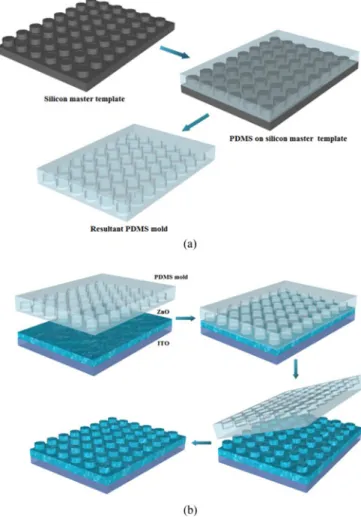
Nanoimprinting of photonic crystal layer has been demon-strated on active layer of both regular and inverted OPV and has been proven to be compatible with large-scale fabrication, as well as with a range of materials [15], [17]. The photonic crys-tal structure used for this experiment was obtained by a method similar to that reported in the literature [23]. The initial step in the process was to prepare the polydimethylsiloxane (PDMS) mold, which was used to create the ZnO photonic crystal layer, as shown in Fig. 1(a). A silicon master template with the de-sired photonic crystal pattern was used to create the PDMS mold. Once satisfactorily produced, this plastic mold could then be used to form photonic crystal structure on any compatible material by contact printing. For forming ZnO photonic crystal structure in electron selective layer of inverted OPV, indium tin oxide (ITO) on glass was used as substrate. ZnO precursor so-lution made using zinc acetate and diethanolamine was dropped on this substrate, while ensuring that the substrate surface was completely covered. The PDMS mold with PC structure was placed on the precursor coated substrate and firmly held in place and annealed on hot plate for the successful transfer of the PC design from the mold to the ZnO layer. The plastic mold was then carefully peeled back to reveal periodic ZnO structures on the ITO substrate. The process is illustrated in Fig. 1(b).
An inverted OPV device structures was used for the studies (ITO/ZnO/P3HT:PCBM/MoO3/Ag). The device schematic is shown in Fig. 2(a). Ultrasonically cleaned ITO on glass was used as the substrate. The electron selective ZnO layer for this device was spin-coated from a ZnO sol-gel prepared by using zinc acetate dihydrate as a precursor, anhydrous ethanol as a solvent, and monoethanolamine as a stabilizing agent [24]. A 1:1 ratio of P3HT:PCBM (40 mg/mL) in cholorobenzene solvent was used as the active layer for the devices. The active layer was
Fig. 1. Schematic representation of the process of fabricating (a) the PDMS mold from the silicon template and (b) the ZnO photonic crystal using the PDMS mold.
Fig. 2. (a) Schematic representation of the fabricated OPV devices. Illustration of (b) the ZnO photonic crystal layer and (c) the planar ZnO layer (reference) used in the devices.
Fig. 3. (a) SEM image and (b) photograph of the ZnO photonic crystal struc-ture formed on ITO coated glass.
spin-coated on the electron selective layer, and a subsequent anneal was performed at 100 °C for 10 min to optimize the active layer morphology. The samples were then transferred to the evaporator for the deposition of MoO3 hole selective layer. Silver electrode was then deposited through shadow mask to define OPV device area. The completed OPV devices were later subjected to postannealing in nitrogen ambient at 160°C for 10 min.
Solar simulator using AM1.5G filter calibrated to obtain simulated light intensity of 100 mW/cm2 was used for the
current density–voltage (J–V) measurements for the fabri-cated devices. From the J–V measurements, the vital device performance parameters, namely, open-circuit voltage (Voc), short-circuit current (Jsc), fill factor (FF), and efficiency (η), were extracted. Incident photon-to-charge conversion efficiency (IPCE) spectra were measured using photovoltaic cell spec-tral response/external quantum efficiency measurement system. PerkinElmer UV/Vis/NIR spectrophotometer system was used for absorption measurements.
III. RESULTS ANDDISCUSSION
SEM image and photograph of the ZnO photonic crystals formed on ITO-coated glass using the method discussed above is shown in Fig. 3. The PC structure is well defined, as can be seen in the SEM image in Fig. 3(a). The iridescence because of diffraction, which is characteristic of photonic crystal structure, is clearly visible in the photograph. Fig. 3(b) is the SEM of the PC layer. The PC structures used for this study had a radius and height of 200 nm, and a pitch of 600 nm.
Guaranteeing a uniform thin ZnO layer below the photonic crystal during imprinting is difficult. A uniform, homogenous, and crystalline layer is imperative for the optimum performance of the device and to ensure that the active layer does not come into direct contact with the ITO. ZnO interlayer affectsVocand FF, and this in turn has an impact on the efficiency of pho-tonic crystal devices. Optimization studies performed showed that the ZnO PC device with underlying ZnO layer thickness of∼80 nm exhibited the best performance (refer to Table II in the Appendix) as it was robust enough to withstand the pho-tonic crystal formation, as well as ensured a good uniform coverage. This translates to a better open-circuit voltage for the devices. Similar optimization studies were systematically
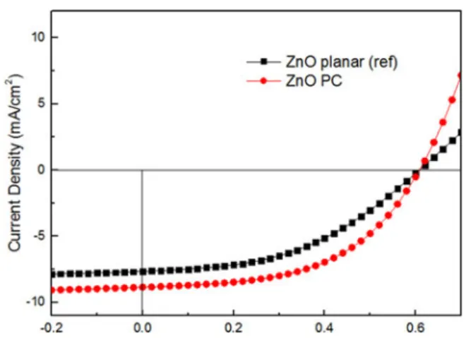
Fig. 4. J–V characteristics of OPV devices with the planar ZnO and the ZnO
photonic crystal electron selective layers. TABLE I
DEVICEPARAMETERS OFOPV DEVICESWITH THEZNO PHOTONICCRYSTAL INELECTRONSELECTIVELAYER ANDTHATWITH THEPLANARZNO
ELECTRONSELECTIVELAYER
Vo c(V) Js c(mA/cm2) FF η
ZnO PC OPV 0.609 −8.939 0.52 2.79%
Reference OPV (with planar 0.613 −7.267 0.59 2.64% ZnO layer)
carried out on the active layer spin-coating speed (refer to Ta-ble III in the Appendix), and the best performance was obtained when a spin speed of 2500 rpm was used for the active layer coating. These optimized parameters were used for the rest of the investigations. Two types of inverted OPV device struc-tures (ITO/ZnO/P3HT:PCBM/MoO3/Ag) were fabricated for these studies. The first type of device used a planar ZnO elec-tron selective layer and was treated as the reference device[see Fig. 2(c)]. The ZnO layer for this device was spin-coated from a ZnO sol-gel. The second type of device had a ZnO photonic crystal structure in its electron selective layer[see Fig. 2(b)].
The resultant J–V characteristics of the devices with planar ZnO and ZnO PC electron selective layers are shown in Fig. 4. Device parameters extracted from the characteristics are listed in Table I. On comparison with the reference planar ZnO device, it can be seen that the efficiency is higher for the ZnO PC device. This increase is because of the enhanced current density offered by the ZnO photonic crystal structure compared with the planar ZnO layer. However, the FF for ZnO PC OPV is lower compared with planar ZnO OPV. The low FF could be because of the nonconformal active layer material filling of the photonic crystal structure [13]. The topography of the ZnO photonic crystal results in nonuniform thickness of active layer across the structure. Such deposition, especially overfill in the troughs, translates to thick active layer in those areas, resulting in increased series resistance, poor charge transport, and efficiency degradation. AlthoughVoc and FF still remain lower than the reference sample and this curbs the overall PCE increase to 6%, the optimized ZnO PC device provides almost 23% increase in the current density.
Fig. 5. IPCE spectra of the reference OPV and the OPV with ZnO photonic crystal layer.
Fig. 6. Absorption spectra of OPVs with and without ZnO photonic crystal layer.
IPCE studies were performed on the reference device and the optimized ZnO PC OPV device. The IPCE spectra obtained is shown in Fig. 5. The IPCE data follows the trend of short-circuit current density and shows an improvement with the use of photonic crystal layer. The photonic crystal structure enables enhanced light trapping, induces increased optical path length, thus increasing the amount of photogenerated charge carriers. This is reflected in both the IPCE and the current density of the ZnO photonic crystal OPV device.
To verify the higher absorption provided by the ZnO pho-tonic crystal layer, absorption measurements were performed on P3HT:PCBM BHJ active layer coated samples of both ZnO PC structure and planar ZnO layer on ITO. The resultant ab-sorption curves are shown in Fig. 6. As can be seen from the curves, the sample with ZnO PC structure showed increased absorption. This enhanced absorbance values in ZnO PC struc-ture is attributed to the incident light trapping induced by the PC topography, resulting in higher absorption in the active layer.
To study the effect of photonic crystal on the absorp-tion of incident solar photons within the active layer, a full
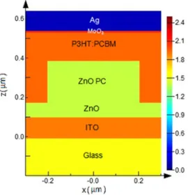
Fig. 7. Refractive index map of device layers at 510 nm.
electromagnetic finite-difference time-domain model using Lumerical software was developed. The 3-D device simula-tion was designed with different layer thicknesses and their respective refractive indexes. Because of the square symme-try of the photonic crystal and incident broadband plane wave source, a single unit cell was considered to run the simulation. In these FDTD simulations, the ZnO photonic crystal structure with square symmetry (period= 600 nm, height = 200 nm, and radii= 200 nm) was used on top of the ZnO layer with vary-ing film thickness 0, 40, and 80 nm, respectively. The periodic boundary conditions were used perpendicular to the organic so-lar cell layers, whereas physically matched layers were used as boundary condition on the top and bottom solar cell design. Two 2-D power monitors were used: the first one located at the boundary between P3HT:PCBM and MoO3 interface and the other located at the boundary between P3HT:PCBM and ZnO nanostructure. These two power monitors helped to evaluate the light absorbed in the P3HT:PCBM active layer because of the presence of ZnO photonic crystal nanostructure on top of the ZnO layer. Another 2-D electric field monitor was used to visu-alize the electric field distribution in the different device layers (in a plane perpendicular to constituent layers of OPV device). Fig. 7 shows the refractive index distribution of different layers at the central wavelength= 510 nm of simulation plane wave spectral range (400–700 nm). The color bar on the right gives the measure of refractive indexes.
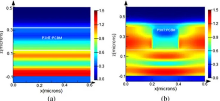
The organic solar cell simulation was carried out for the de-vices with both planar and photonic crystal ZnO electron selec-tive layers. Fig. 8 shows the electric field distribution inside the two simulated OPV devices at the source wavelength of 510 nm. In Fig. 8(a), the electric field distribution is computed within the reference device, which shows that the incident electric field de-cays within the active layer. The position of active layer within the device is depicted by white line everywhere. In Fig. 8(b), because of the presence of the 2-D ZnO PC on top of the 80-nm ZnO layer, the incident field is trapped and guided, which in turn increases the absorption within the active layer of the device.
Fig. 8. Electric field distribution in OPVs with (a) the planar ZnO and (b) the ZnO photonic crystal electron selective layers.
IV. CONCLUSION
In summary, the photonic crystals embedded in the electron selective layer of the OPV lead to enhancement of current den-sity by virtue of field localization. Optimized OPVs with these PC structures can effectively trap incident light and increase absorption in active layer. Numerical studies further support this finding. Compared with the OPV devices with planar ZnO electron selective layers, the ZnO PC, thus, provides enhanced performance and the use of such photonic structures may also be readily extended to any metal oxide interlayer employed in OPV structures.
APPENDIX TABLE II
DEVICEPARAMETERS OFZNO PHOTONICCRYSTALOPVSWITHUNDERLYING
ZNO LAYER OFDIFFERENTFILMTHICKNESS
IZO layer spin speed Vo c(V) Js c(mA/cm2) FF η ZnO PC OPV with no 0.507 −6.599 0.44 1.46% underlying ZnO layer
ZnO PC OPV with one 0.554 −7.421 0.45 1.87% underlying ZnO layer
ZnO PC OPV with two 0.608 −8.203 0.44 2.20% underlying ZnO layers
Reference OPV with 0.613 −7.267 0.59 2.64% planar ZnO layer
TABLE III
DEVICEPARAMETERS OFZNO PHOTONICCRYSTALOPVSWITHACTIVE
LAYERSPIN-COATED ATDIFFERENTSPIN-COATINGSPEEDS
Vo c(V) Js c(mA/cm2) FF η 800–1000 rpm 0.572 −7.693 0.42 1.86% 2000 rpm 0.608 −8.203 0.44 2.20% 2500 rpm 0.609 −8.939 0.52 2.79%
REFERENCES
[1] G. Yu, J. Gao, J. C. Hummelen, F. Wudl, and A. J. Heeger, “Polymer photovoltaic cells: Enhanced efficiencies via a network of internal donor– acceptor heterojunctions,” Science, vol. 270, pp. 1789–1791, 1995. [2] J. Zhao et al., “Efficient organic solar cells processed from hydrocarbon
solvents,” Nature Energy, vol. 1, 2016, Art. no. 15027.
[3] K. Zhang et al., “High-Performance polymer tandem solar cells employing a new n-type conjugated polymer as an interconnecting layer,” Adv. Mater., vol. 28, pp. 4817–4823, 2016.
[4] M. Niggemann, M. Glatthaar, A. Gombert, A. Hinsch, and V. Wittwer, “Diffraction gratings and buried nano-electrodes—Architectures for or-ganic solar cells,” Thin Solid Films, vols. 451/452, pp. 619–623, 2004. [5] C. Cho et al., “Random and V-groove texturing for efficient light trapping
in organic photovoltaic cells,” Solar Energy Mater. Solar Cells, vol. 115, pp. 36–41, 2013.
[6] R. Seung-Bum, Z. Shanbin, S. R. Scully, M. D. McGehee, and P. Peumans, “An effective light trapping configuration for thin-film solar cells,” Appl.
Phys. Lett., vol. 91, 2007, Art. no. 243501.
[7] M. Niggemann et al., “Functional microprism substrate for organic solar cells,” Thin Solid Films, vols. 511/512, pp. 628–633, 2006.
[8] S. I. Na et al., “Surface relief gratings on poly(3-hexylthiophene) and fullerene blends for efficient organic solar cells,” Appl. Phys. Lett., vol. 91, Oct 2007, Art. no. 173509.
[9] D. H. Wang, A. K. K. Kyaw, Q. G. Du, D.-G. Choi, and J. H. Park, “Tailoring of the plasmonic and waveguide effect in bulk-heterojunction photovoltaic devices with ordered, nanopatterned structures,” Organic
Electron., vol. 15, pp. 3120–3126, Nov. 2014.
[10] D.-H. Ko et al., “Light-trapping nano-structures in organic photovoltaic cells,” J. Mater. Chem., vol. 21, pp. 16293–16303, 2011.
[11] L. Zeng et al., “Efficiency enhancement in Si solar cells by textured photonic crystal back reflector,” Appl. Phys. Lett., vol. 89, Sep. 2006, Art. no. 111111.
[12] S. B. Mallick, M. Agrawal, and P. Peumans, “Optimal light trapping in ultra-thin photonic crystal crystalline silicon solar cells,” Opt. Express, vol. 18, pp. 5691–5706, Mar. 2010.
[13] K. S. Nalwa, J. M. Park, K. M. Ho, and S. Chaudhary, “On realizing higher efficiency polymer solar cells using a textured substrate platform,” Adv.
Mater., vol. 23, pp. 112–116, Jan 2011.
[14] D. Duche et al., “Slow Bloch modes for enhancing the absorption of light in thin films for photovoltaic cells,” Appl. Phys. Lett., vol. 92, May 2008, pp. 7670–7681.
[15] D. H. Ko, J. R. Turnbleston, W. Schenck, R. Lopez, and E. T. Samulski, “Photonic crystal geometry for organic polymer: Fullerene standard and inverted solar cells,” J. Phys. Chem. C, vol. 115, pp. 4247–4254, Mar. 2011. [16] D.-H. Ko et al., “Photonic crystal geometry for organic solar cells,” Nano
Lett., vol. 9, pp. 2742–2746, Jul. 2009.
[17] Y. Liu et al., “Effects of nano-patterned versus simple flat active layers in upright organic photovoltaic devices,” J. Phys. D: Appl. Phys., vol. 46, 2013, Art. no. 024008.
[18] M. S. White, D. C. Olson, S. E. Shaheen, N. Kopidakis, and D. S. Ginley, “Inverted bulk-heterojunction organic photovoltaic device using a solution-derived ZnO underlayer,” Appl. Phys. Lett., vol. 89, 2006, Art. no. 143517.
[19] A. K. K. Kyaw et al., “An inverted organic solar cell employing a sol-gel derived ZnO electron selective layer and thermal evaporated MoO3 hole selective layer,” Appl. Phys. Lett., vol. 93, 2008, Art. no. 221107. [20] S. K. Hau et al., “Air-stable inverted flexible polymer solar cells using
zinc oxide nanoparticles as an electron selective layer,” Appl. Phys. Lett., vol. 92, 2008, Art. no. 253301.
[21] C. F. Zhang, H. L. You, Z. H. Lin, and Y. Hao, “Inverted organic pho-tovoltaic cells with solution-processed zinc oxide as electron collecting layer,” Jpn J. Appl. Phys., vol. 50, Aug. 2011, Art. no. 082302. [22] Z. F. Liu, Z. G. Jin, W. Li, and J. J. Qiu, “Preparation of ZnO porous
thin films by sol-gel method using PEG template,” Mater. Lett., vol. 59, pp. 3620–3625, Dec. 2005.
[23] Z. Kyaw et al., “Room-temperature larger-scale highly ordered nanorod imprints of ZnO film,” Opt. Express, vol. 21, pp. 26846–26853, Nov. 2013. [24] A. Nirmal, A. K. K. Kyaw, X. W. Sun, and H. V. Demir, “Microstruc-tured porous ZnO thin film for increased light scattering and improved efficiency in inverted organic photovoltaics,” Opt. Express, vol. 22, pp. A1412–A1421, Oct. 2014.