Nanoplasmonic three-dimensional surfaces
with strong surface-normal electric field enhancement
Kıvanç Güngör1, Emre Ünal1, and Hilmi Volkan Demir1,2
1Department of Electrical and Electronics Engineering, Department of Physics, and UNAM - Institute of Materials Science and Nanotechnology Bilkent University, Ankara, Turkey TR-06800
2LUMINOUS! Center of Excellence for Semiconductor Lighting and Displays, Microelectronics Division, School of Electrical and Electronics Engineering, and Physics and Applied Physics Division, School of Physical and Mathematical Sciences, Nanyang Technological University,
Nanyang Avenue, Singapore 639798, Singapore Email: [email protected] and [email protected]
Abstract: Conventional plasmonic structures provide field enhancement in the plane. The
proposed nanoplasmonic three-dimensional surfaces, with unity coverage in the plan-view, enable surface-normal enhancement and achieve 7.2-fold stronger maximum field enhancement compared to the two-dimensional counterparts.
Two-dimensional (2D) plasmonic nanostructures implemented on a planar surface can typically reach only a low level of surface coverage, which is commonly significantly less than 100%. When a periodic layout is used as a repeating 2D pattern, as is frequently the case, (although the periodicity is not a requirement), the resulting plasmonic array inherently yields a duty cycle considerably less than unity (usually close to 0.5) [1,2]. Also, the resulting field localization occurs mostly in the plane in the vicinity of sharp corners and between small gaps of their nanopatterns on the flat surface. As a result, the surface coverage of the nanopatterned plasmonic structures on a planar surface has intrinsically been limited and the field enhancement across their layout has been possible mostly in the plane (and slightly above it). In this work, we proposed and demonstrated nanoplasmonic three-dimensional (3D) surfaces designed and fabricated on a non-planar surface that enables strong field enhancement in the surface-normal direction, while allowing for the surface coverage of the substrate close to unity in the plan-view. Also, the process flow developed specifically for the proposed 3D surfaces requires fewer fabrication steps than their 2D counterparts, reducing the complexity and cost of their nanofabrication.
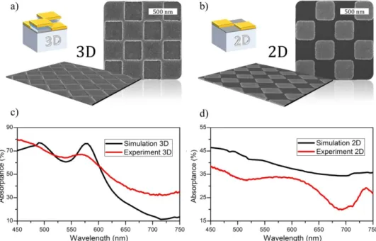
Figures 1(a) and 1(b) show scanning electron microscopy (SEM) images of the 3D and 2D model systems, respectively, with the corresponding illustrative unit cell sketches. These nanostructures were fabricated using electron beam lithography (EBL) on thin chromium layer coated fused quartz wafers. The interplanar spacing layers in the 3D structure consist of bilayer PMMA, which was also used as the EBL resist. Numerical simulations and experiments were compared by observing the far-field absorption of these 3D and 2D structures, presented in Figures 1(c) and 1(d). The two-fold rotational symmetry of these plasmonic structures led to polarization independent behavior, unlike the common 1D gratings having strong polarization dependence [3].
Fig. 1. Perspective and plan-view SEM images of the 3D (a) and 2D (b) plasmonic model systems. Experimentally measured and numerically simulated far-field absorptance of these 3D (c) and 2D (d) structures.
316
TuH1.2 (Contributed) 9:00 AM – 11:15 AM
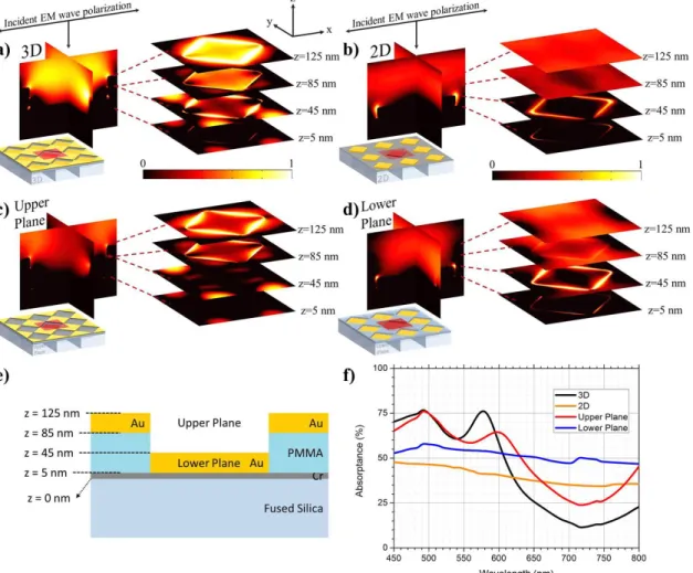
Figures 2(a)-2(d) present the cross-sectional near-field electric field intensity distribution maps of the 3D and 2D model systems as well as those of the upper plane and the lower plane components, together making up the full 3D structure, with respect to the incoming source intensity in the logarithmic scale [4]. Here the upper plane contains the partial structure that is left after removing the gold plane between z=5 and z=45 nm; and, in a complementary fashion, the lower plane consists of the partial structure remaining after the gold layer between z=85 nm and z=125 nm is removed (Figure 2(e)). These simulations are performed using a commercially available FDTD solver (Lumerical Inc.) using 3D simulation environment under impinging plane wave. From Figure 2(f), it is evident that the resonance of the 3D structure results from the coupling between the upper and lower plane structures since the plasmonic resonance of the upper plane structure blue-shifts and develops a stronger resonance. Figure 2(a) shows that the 3D structure is superior to the other structures, with its volumetric field enhancement reaching a maximum field enhancement factor 7.2 times larger than that of the 2D structure.
Fig. 2. Numerical simulation results displaying electric field intensity distributions for the 3D (a), the 2D (b), the upper plane (c) and the lower plane (d) structures. Important positions along z-direction and the components of the upper and lower plane structures are illustrated (e).
Computed absorptance of all of these modeled structures, showing coupling between the upper and lower planes in the 3D structure (f).
In conclusion, the proposed nanoplasmonic 3D surfaces provide volumetric electric field intensity enhancement, significantly stronger than the 2D planar structures, as verified by the numerical simulations agreeing well with the experimental far-field measurements. With the surface-normal field enhancement, the volumetric field enhancement factor of the 3D model system is found to be 7.2 times larger than the 2D counterpart. This showcases the strength and potential of the nanoplasmonic 3D surfaces.
This work is supported by National Research Foundation under Grant No. NRF-RF-2009-09 and NRF-CRP-6-2010-2, and also by EU-FP7 Nanophotonics4Energy-NoE. H.V.D. acknowledges support from ESF-EURYI and TUBA-GEBIP, K.G. from TUBITAK-BIDEB.
[1] K. Aydin, V. E. Ferry, R. M. Briggs, and H. Atwater, Nat. Comm., 2, 517 (2011).
[2] K. Ueno, S. Juodkazis, V. Mizeikis, K. Sasaki, and H. Misawa, Adv. Mat., 20, 26–30 (2008). [3] E. Hwang, I. I. Smolyaninov, and C. C. Davis, Nano Lett., 10, 813–20 (2010).
[4] K. Gungor, E. Unal, and H. V. Demir, submitted.
317 978-1-4577-1507-5/13/$26.00 ©2013 IEEE