Defect Reduction of Ge on Si by Selective Epitaxy and Hydrogen Annealing
Hyun-Yong Yu1, Jin-Hong Park1, Ali K. Okyay1,2 and Krishna C. Saraswat1
1Department of Electrical Engineering, Stanford University, Stanford, CA 94305 USA 2Department of Electrical and Electronics Engineering, Bilkent University, Ankara,
06800 Turkey
We demonstrate a promising approach for the monolithic integration of Ge-based nanoelectronics and nanophotonics with Silicon: the selective deposition of Ge on Si by Multiple Hydrogen Annealing for Heteroepitaxy (MHAH). Very high quality Ge layers can be selectively integrated on Si CMOS platform with this technique. We confirm the reduction of dislocation density in Ge layers using AFM surface morphology study. In addition, in situ doping of Ge layers is achieved and MOS capacitor structures are studied.
Introduction
Many of the true breakthroughs in the technology are related to materials and the understanding of their properties. Emergence of new semiconductor materials systems, especially in crystalline form, strongly shapes future photonics and electronics. Today, among such new material systems, Ge heteroepitaxy on Si is very promising both for high performance Ge metal-oxide-semiconductor (MOS) transistors(1,2) and as a potential path for integrating optoelectronic devices with Si MOS technology(3). For greater ease of integration with Si MOS, the precise control and process compatibility are required. It is hence crucial to be able to grow high quality SiGe layers selectively on Si.
In this paper, we demonstrate the selective Multiple Hydrogen Annealing for Heteroepitaxy (MHAH), a promising approach for the integration of SiGe based electronics on Si VLSI platform. The selective growth mechanism combined with hydrogen annealing steps yields high quality Ge on Si. This technique yields Ge layers with very low dislocation density and surface roughness as confirmed by AFM surface morphology study, and capacitance-voltage (C-V) characteristics of n-type MOS capacitors (MOSCAP). In addition, the combined study of the geometry of the grown layers, the growth rates and conditions, shed light on the mechanisms of the selective Ge growth.
Experiment
A 300-nm-thick SiO2 film was thermally grown on p-type (100) Si substrate at 1100oC.
The SiO2 film was then patterned by a combination of dry followed by wet-etching to
define desired locations for Ge growth. The wafer was dipped in 50:1 H20:HF for 30 sec
and immediately loaded into an Applied Materials Centura epitaxial reactor. A Hydrogen bake at 900oC was carried out to ensure no native oxide remained on the Si surface in the patterned SiO2 windows. In order to increase the film quality, a very thin Si epi-layer was
first grown for 90 sec at 700oC with DCS (dichlorosilane) as the reaction species. DCS has good selectivity to SiO2, which only allows the thin Si layer to be selectively grown
on the patterned Si surface. The initial Ge film was grown at 400oC and 8 Pa, yielding a 800-nm-thick film. This was followed by annealing in H2 ambient for 30 min at 825oC.
The growth temperature was increased to 600 oC for the last Ge layer. Finally, a 15 min H2 bake at 750oC completed the process. We have grown blanket Ge films on
unpatterned Si substrates as control samples. AsH3 was mixed with GeH4 for in situ
doping. Four point probe method was used to measure the sheet resistance of doped Ge layers and extract the electrically active doping level in the films.
Results and Discussion
Selective Growth Model
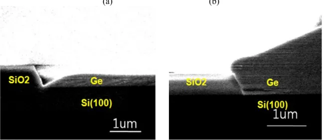
Figure 1 shows the geometrical shape of the resulting Ge film depending on the process temperature. Figure 1(a) shows the cross-sectional SEM image of the sample grown at 400oC in a 15µm-wide SiO2 window. At 400oC, the growth in the <100>
direction is dominant while <311> direction facets are observed giving the film a trapezoidal shape. This is primarily due to the relatively slow growth rate along the <311> direction under these conditions, and it can be explained by surface migration (4). As the deposition time is increased, the layer forms into a pyramid-like structure. Once the full pyramid is formed, there is no significant increase in the layer thickness with further growth time. However, when the growth temperature is raised to 600oC, the resulting film has a different shape (Figure1(b)). This is due to high growth rates in both the <311> direction (94 nm/min) and the <100> direction (480 nm/min). Surface migration is restricted at higher temperatures by an excessive number of nucleation centers due to a high number of reactive species arriving at the surface (4).
(a) (b)
Figure 1. Cross-sectional SEM images in growth temperatures of (a) 400 oC and (b) 600
oC.
Surface morphology of selective and blanket Ge growth
Atomic Force Microscopy (AFM) was used to study the surface morphology of the grown Ge layers. Figure 2 compares AFM images of blanket film growth (Figure 2(a)) vs. selective growth (Figure 2(b)). In both cases, the first and the second layers are grown at 400oCwith intermediate hydrogen annealing steps. A third layer is grown at 600oC. The pit density in blanket Ge layers is 1x107cm-2 while relatively small pit density is observed
in Figure 2(b). The threading dislocation density can be estimated by the AFM observation of the surface morphology because it is influenced by threading dislocations (5). The low pit density (2x106cm-2) of Fig. 2(b) means that the threading dislocation density of selective Ge growth is relatively low compared to that of blanket Ge growth.
(a) (b)
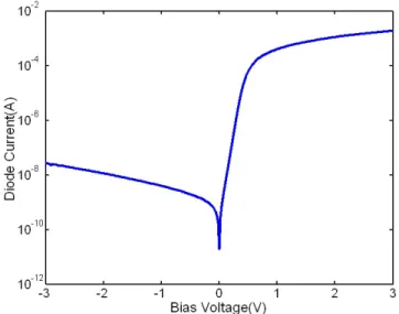
Figure 2. AFM images showing the surface morphology of (a) bulk Ge growth and (b) selective Ge growth. The pit density of (a) is 1x107cm-2 while that of (b) is 2x106cm-2. The current-voltage (I-V) characteristic of the Schottky diode is an indication of material quality. Figure 3 plots the measured I-V characteristics of the metal semiconductor (MS) (Ti-Ge) Schottky diode for 400oC and 600oC multi-step growth. The layers were grown
in a 10µmx10µm SiO2 window followed by hydrogen annealing. The I-V characteristic of
the Ti-Ge junction shows a Schottky diode behavior with decent rectification which is another indication of the low defect density of the selective MHAH-Ge substrate.
In situ Arsine doping of Ge
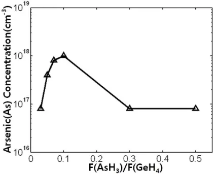
Ge layers are grown at 600℃ directly on p-type (100) Si substrate. The flow rate of arsine (AsH3) is varied while that of germane (GeH4) is fixed during growth. Finally, the
samples are annealed in hydrogen ambient at 825 oC Figure 4 shows the electrically active arsenic (As) concentration, obtained from the sheet resistance measurements, as a function of the relative flow rate of AsH3 and GeH4 gases. As the partial pressure of
AsH3 is increased, the concentration of As increases reaching a maximum of 1x1018 cm-3.
With further increase of the partial pressure of AsH3, a poly-crystalline growth is
observed with the electrically active As concentration decreasing. The initial increase in the As concentration is owing to an increased supply of As ions with higher AsH3 partial
pressure. The subsequent reduction in the electrically active As concentration is attributed to the formation of grains and grain boundaries during the poly-crystalline growth. The lowest As concentration (8x10¹⁶/cm3) is obtained at 0.03 mass flow ratio with very uniform ion concentration over the wafer. However, large variation in the ion concentration over the wafer is observed below this mass flow ratio.
Figure 4. Arsenic ion concentration obtained in Arsine doped Ge layers grown at 600℃ as a function of the F(AsH3)/F(GeH4) mass flow ratio.
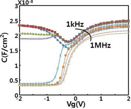
MOS capacitors using GeOxNy and Al2O3 as the dielectric and aluminum(Al) as the gate
electrode were fabricated. The selective epitaxial Ge layer was in situ doped with As during the deposition step. GeOxNy was grown directly by oxidation followed by
nitridation at 600℃ in a rapid thermal processing system using ammonia and 200 nm of Al was deposited. Figure 5 shows the C-V characteristics from 1kHz to 1MHz. Beyond 100 kHz sweep, a kink is observed in the depletion region. This is due to the high interface states at the GeOxNy/Ge interface (6). This C-V characteristics verify the low
Figure 5. C-V characteristics of n-type epi-Ge MOS capacitor structure using GeOxNy
and Al2O3 gate dielectric and Al gate electrode. Conclusion
In conclusion, high quality Ge can be selectively grown on Si by MHAH through a SiO2
masking pattern. Two different growth mechanisms were observed at 400oC and 600oC resulting from relative growth rates in <311> and <100> directions. The hydrogen annealing and the selective growth can be used to reduce the dislocation density and the surface roughness. The in situ As doping of Ge at 600oC shows the ion concentration dependency on the mass flow ratio. In addition, n-type MOS capacitor is demonstrated on the in-situ doped selective epitaxial Ge film. This selective MHAH Ge growth and in situ doping can be used for integrating advanced Ge optoelectronics with Si-based electronic device technologies.
Acknowledgments
The authors would like to thank The FCRP Interconnect Focus Center and PhotonicIC Corporation for funding this research project.
References
1. M. Lee, C.W.Leitz, Z. Cheng, A. J. Pitera, T. Langdo, M. T. Currie, G. Taraschi, E.A. Fitzgerald, and D. A. Antoniadis, Appl. Phys. Lett. 79, 3344 (2001).
2. C. O. Chui, H. Kim, D. Chi, B. B. Triplett, P. C. McIntryre, and K. C. Saraswat. Tech. Dig. Int. Electron Device Meet. 2001, 437.
3. E. A. Fitzgerald, Y. H. Xie, D. Monroe, P. J. Silverman, J. M. Kuo, A. R. Kortan, F. A. Thiel, and B. E. Weir, J. Vac, Sci, Technol. B 10, 1807 (1992).
4. S. Kobayashi, M. Cheng, A. Kohlhase, T. Sato, J. Murota and N. Mikoshiba, Journal of Crystal Growth Vol.99 pp.259-262 (1990)
5. T. Egawa, A. Sakai, T. Yamamoto, N.Taoka, O. Nakatsuka, S. Zaima, and Y. Yasuda, Appl. Surfac Science 224, 104(2004)