8:45am
-
9:lSamThC2
High-Performance ITO-AIAsIGaAs based Resonant
Cavity Enhanced Schottky Photodiodes
Schottky photodiodes with thin absorption regions are very attractive for applications where ultrafast detection is desired. Ultrafast Schottky photodiodes with 3-dB bandwidths exceeding 200 GHz have already been demonstrated [I]. However, their efficiency performance is poor, mainly due to thin absorption regions needed for short transit times. The bandwidth-efficiency (BWE) product, which denotes the photodetector performance, is limited for such conventional photodiodes. Resonant cavity enhanced (RCE) photodetection scheme offers a clever solution to overcome this limitation [2]. The active device structure is placed inside a Fabry-Perot microcavity, so that the optical field (and therefore the quantum efficiency) is enhanced at the resonant wavelengths. RCE photodetector research has demonstrated very high BWE products, which could not be achieved with conventional detectors. Recently, we have fabricated RCE type Schottky and p-i-n photodiodes with 25 GHz and 46 GHz BWE products respectively [3-41. The main factor which limits us from reaching higher BWE products in our RCE-Schottky design is the semi-transparent Schottky metal, Au, which also serves as the top mirror of the resonant cavity. Despite its good reflecting property, Au is a strong absorber and its surface roughness causes back-scattering of incident light which decreases the efficiency. It is shown that transparent conducting indium-tin-oxide (ITO) is a potential alternative to thin semi-transparent Au as a Schottky- barrier contact material [5]. High-performance ITO- based conventional Schottky photodiodes are demonstrated using different material systems [6-71. In this paper, we report our efforts on ITO- AlAs/GaAs based RCE Schottky photodiodes for operation at the first optical communication window (840 nm).
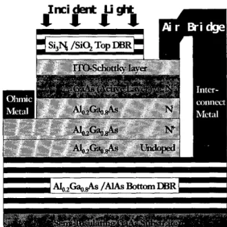
The device structure (shown in Figure 1) is designed to achieve a low-loss (high Q) cavity around 840 nm. The layers are grown by MBE on a semi- insulating GaAs substrate. The resonant cavity is formed by an Al, 2Ga, ,As/AlAs DBR bottom mirror and a PECVD-grown Si,N4/Si0, DBR top mirror, both centered at 840 nm. At the operation wavelength, only the active GaAs region absorbs the optical excitation.
Ekmel Ozbaya, Necmi Biyiklib, Ibrahim Kimukina, and
Orhan Ayturb
The samples were fabricated by a microwave- compatible fabrication process, where standard photolithography, wet/dry chemical etching and thick metal lift-off processes are utilised. The Schottky contact is formed by a 100 nm thick IT0 film, which is sputter-deposited in an argon atmosphere. Dielectric top DBR is grown by using PECVD at 250°C chamber temperature. To reduce the parasitic capacitance, the Schottky (ITO) layer is connected to the contact pads by an Ti-Au airbridge. Figure 1 also shows the contact structure of a fabricated RCE Schottky photodiode.Photo response measurements were carried out in 750-900 nm wavelength range, by using a tungsten- halogen projection lamp as the light source and a single pass monochromator. Output of the monochromator was coupled to a multimode fiber. The monochromatic light was delivered to the devices by a lightwave fiber probe, and the electrical characterization was carried out on a probe station.
Figure 1: The schematic cross-section of the fabricated RCE Schottky photodiode.
a Department of Physics, Bilkent University, Bilkent, Ankara 06533, Turkey
Department of Electrical and Electronics Engineering, Bilkent University, Bilkent, Ankara 06533, Turkey
12
i ! : ! i ! : ! i I1. I’ i
800
840
880”
760Wavelengttr(nm)
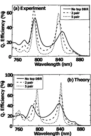
Figure 2: (a) Experimental and (b) theoretical photoresponse of the RCE Schottky photodiode.
Figure 2(a) and 2@) shows the measured and calculated spectral quantum efficiencies of devices with different top mirrors respectively. We used transfer matrix method based simulations in our theoretical calculations. Before top DBR deposition, the measured peak quantum efficiency was 33%, while the calculations predicted 43%. Pair-by-pair this value increased to 41%, 48%, 54%, 58%, and 59% for 1 to 5 pair Si,N4/Si0, top DBR. The maximum peak efficiency measured is 59% with 5 pair top DBR, where we theoretically predict a peak value of 84%. Although the discrepancy between experiment and theory is quite large, a nearly parallel enhancement of both initial efficiency values as a function of top DBR pair number is observed. Moreover, our experimental results confirmed that the optimum efficiency condition, &p=%otexp(-2ad) was satisfied with a 5
pair top DBR. FWHM of the resonant peak decreased from 30 nm to 10 nm, while at the same time wavelength selectivity increased by a factor of -8 which are in good agreement with our theoretical expectations.
High speed measurements were made with 1 psec FWHM optical pulses obtained from a Ti-Sapphire laser operating at 840 nm.
0
40
8 0 1 z o 1 ~ 2 0 0
Time @sec)
Figure 3: Pulse response of the sample
Figure 3 shows the temporal response of a small area photodiode measured by a 50 GHz sampling scope. The measured photodiode output has a 20 psec FWHM at 2V bias. At zero bias the device had a FWHM of 35 psec. We expected better results if we were able to apply 4-5 volts bias but the leakage in device capacitors prevented us from this. The Fourier transform of the data has a 3-dB bandwidth of -20 GHz.
This work was supported in part by the Turkish Scientific and Technical Council under Project 197- E044, in part by the NATO Grant No. Sfp971970, and in part by the National Science Foundation International Collaborative Research under Grant INT-960 1770.
REFERENCES
[l] E. Ozbay, K. D. Li, and D. M. Bloom, IEEE
Photon. Technol. Lett., vol. 3 , pp. 570-572, 1991.
[2] M. S . h l u and S . Strite, “Resonant cavity enhanced (RCE) photonics devices,” J. Appl. Phys.
[3] M. S . Unlu, M. Gokkavas, B. M. Onat, E. Ata, E. Ozbay, R. P. Mirin, K. J. Knopp, K. A. Bei-tness, and D. H. Christensen, Applied Physics Letters, volume
72, p. 2727 (1 998).
[4] E. Ozbay, N. Biyikli, I. Kimukin, O.Aytur, M.
Gokkavas, G. Ulu, M. S . Unlu, R. P. Mirin, and D. H. Christensen, Applied Physics Letters, volume 74, p. 1072 (1999).
[ 5 ] D. G. Parker, GECJ. Res., vol. 5 , p.116, 1987. [6] D. G. Parker, P. G. Say, A. M. Hansom, and W. Sibbet, Electron. Lett., vol. 23, p.527, 1987.
[7] W. A. Wohlmuth, J. W. Seo, P. Fay, C. Caneau, and I. Adesida, IEEE Photon. Technol. Lett., vol. 9,
Rev., vol. 78, pp. 607-639, 1995.
pp. 1388-1390, 1997.