Plasmonic Nanoslit Enhanced Metal-Semiconductor-Metal
Photodetectors
Sukru Burc Eryilmaza), Ali K. Okyayb)
Department of Electrical and Electronics Engineering, UNAM-Institute of Materials Science and Nanotechnology, Bilkent University, Ankara 06800, Turkey
a) Author to whom correspondence should be addressed: [email protected] b) Electronic mail: [email protected]
Abstract: We computationally show that metallic nanoslitsintegrated on Germanium metal-semiconductor-metal photodetectors show absorption enhancement up to 8 for TM-polarization in the communications C-band due to interference of horizontal surface plasmons.
OCIS codes: 040.5160; 130.0250; 250.5403
Semiconductor industry has continuously scaled down electronic devices, significantly improving device level performance; but the same is not true for the on-chip electrical interconnections. The high frequency nature of photonics make optical interconnects a natural candidate for high capacity information transfer medium, resulting in an avalanching interest in demonstrating efficient Ge-based optical detection closely integrated with Silicon and Silicon based waveguide technologies to realize integrated optoelectronics [1-3].
It is desirable that the finger spacing and active layer thickness in metal-semiconductor-metal (MSM) photodetectors be reduced for high-speed operation while maintaining the efficiency of the device. Despite earlier reports in the literature on electromagnetic resonance modes in MSM structures [4,5], a complete study does not exist and there is a need for a thorough investigation of plasmonic gratings integrated with MSM photodetectors.
For a proof-of-concept demonstration in the near infrared (NIR) photodetectors, we computationally studied Germanium based MSM photodetectors integrated with gold gratings as shown in Fig. 1. We computed the field
Fig. 1. (a) MSM photodetector structure aeriel view (top) and cross-section along AB (bottom) (b) Simulated structure
for allowed HSP modes with structural parameters. (c) Simulated structure for suppressed HSP modes.
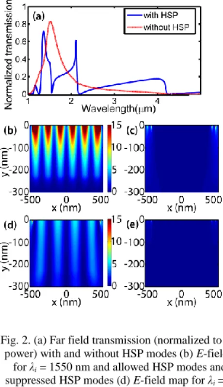
Fig. 2. (a) Far field transmission (normalized to source power) with and without HSP modes (b) E-field map
for λi = 1550 nm and allowed HSP modes and (c)
suppressed HSP modes (d) E-field map for λi = 2110
nm and allowed HSP modes and (e) suppressed HSP modes. E-field intensity values are clipped at 15 in the
color scale. field intensity is normalized to the E-field intensity of the source. All E-fieldmaps use the
same color scale.
JWA39.pdf 1 9/30/2011 11:11:21 AM
FIO/ LS Technical Digest @ 2011 OSA
maps of metallic gratings integrated on Ge based photodetectors and investigated the relative contribution to optical absorption enhancement with respect to the bare device using two-dimensional finite-difference time-domain (FDTD) method (Lumerical Solutions Inc., Canada).
We first studied the contribution of vertical cavity modes (CM) and horizontal surface plasmon modes (HSP) on the transmission and reflection of the incident light assuming a nondispersive and lossless Germanium region. The normalized transmission vs the wavelength of the light with and without suppressing HSP’s is shown in Fig. 2(a). Surface plasmon oscillations tend to reduce the transmitted far field intensity except for a narrow range of wavelengths, as observed by Crouse et. al. [4] However, MSM and other high-speed photodetectors are essentially surface devices with thin active layers and the field intensity in the thin active layer is crucial. The near field intensity
in the vicinity of the surface of such structures is dramatically different, in favor of HSPs, as shown in Fig. 2(b) and 2(d) (allowing HSPs) and 2(c) and 2(e) (suppressing HSPs). The standing wave pattern of the field at the surface is
due to interference of surface plasmon oscillations from adjacent gratings and the ends of the metallic slits.
We comparatively studied the MSM photodetector performance with metallic slits with respect to the case of the starting photodetector with no metallic gratings (dubbed “bare” device) by parametrically optimizing the metallic slits for maximum absorption enhancement in the active region. In absorption enhancement calculations, optical coefficients of strained Germanium [6] grown on Silicon and Au [7] is used for real and imaginary refractive indices of Germanium and Gold material, respectively. Absorption enhancement for metallic structures with structural parameters (d, P, t) in Fig. 1(b) is computed as the ratio of overall absorption of Ge-layer with metallic structure, to the absorption of the same Ge-layer with no metallic structure (bare device). Maximum absorption enhancement of 8-fold (for a 300-nm-thick active layer) at the illumination wavelength of λi = 1550 nm is obtained for (d, P, t) = (75 nm, 1000 nm, 260 nm). Silicon layer is omitted in these computations, the total absorption of the structure with the
optimized grating decreases by 0.4 % when Silicon layer is also included. The absorption in the semiconductor is significantly inhibited for TE-polarized illumination. Therefore, the overall enhancement factor for un-polarized illumination is around 4.
The absorption enhancement is greater for photodetectors with active areas thinner than 300 nm. HSP modes enhance the absorption for photodetectors with active layer thicknesses even greater than 1 m, complementing the claims in related reports on the role of the HSP oscillations [4].
We analyze and utilize surface plasmon modes for the design of Germanium MSM photodetectors operating in the telecommunications bands. Absorption enhancement factor up to 8 was obtained. Results are interpreted as a combined effect of horizontal surface plasmon modes as well as vertical cavity modes.
This work was supported by TUBITAK 108E163, 109E044, EU FP7 PIOS 239444. The authors acknowledge Turkish Ministry of Industry and Trade seed fund and TUBITAK BIDEP.
REFERENCES
[1] M. Oehme, J. Werner, E. Kasper, M.Jutzi, and M. Berroth, "High bandwidth Ge p-i-n photodetector integrated on Si," Appl. Phys. Lett. 89, 071117 (2006).
[2] J. Michel, J. Liu, and L. C. Kimerling, "High-performance Ge-on-Si photodetectors," Nature Photonics 4, 527 (2010).
[3] S. Assefa, F. Xia, and Y. A. Vlasov, "Reinventing germanium avalanche photodetector for nanophotonic on-chip optical interconnects," Nature 464, 80 (2010).
[4] D. Crouse and P. Keshavareddy, "Role of optical and surface plasmon modes in enhanced transmission and applications," Opt. Express 13, 7760 (2005).
[5] J. Hetterich, G. Bastian, N. A. Gippius, S. G. Tikhodeev, G. von Plessen, and U. Lemmer, "Optimized design of plasmonic MSM photodetector," IEEE J. Quantum Electron 43, 855 (2007).
[6] A. K. Okyay, A. Nayfeh, T. Yonehara, A. Marshall, P. C. McIntyre, and K. C. Saraswat, "High-efficiency metal-semiconductor-metal photodetectors on heteroepitaxially grown Ge on Si," Opt. Lett. 31, 2565 (2006).
[7] E. D. Palik, Handbook of Optical Constants of Solids (Academic, New York, 1985).
JWA39.pdf 2 9/30/2011 11:11:21 AM
FIO/ LS Technical Digest @ 2011 OSA