©BEYKENT UNIVERSITY
CHIP RESISTOR AND NEGATIVE CAPACITOR
LOADED
RECTANGULAR BROAD BAND MICROSTRIP
ANTENNAS
Adnan KAYA
Department of Electronics and Communication
Engineering Süleyman Demirel University
Isparta, Turkey, 32260
[email protected]
ABSTRACT
Various communication systems require single radiating element operating in wide band. In this paper, a novel active integrated single microstrip antenna is proposed and its radiation pattern and gain performance is optimized with analysis. The reactive loading is provided by a negative capacitor section embedded within the patch. The active negative capacitor is made of a field-effect transistor that exhibits negative resistance as well as capacitance. It can, therefore, compensate the loss of an inductor. A microstrip patch operating at 10.5 GHz having 12.2% bandwidth has been utilized as a reference antenna. With the proposed antenna design, the antenna radiation pattern can be as large as about 1.5 times that of an antenna without reactive loading. In addition, it has been shown that active compensation significantly improves the matching level.
Key words: Matchineg level, active matching, negative active capacitance.
ÖZET
Geniş bant da çalışan çeşitli iletişim sistemlerinde tek ışıma yapan yapılara gereksinim vardır. Bu çalışmada anten ışıma örüntüsünü ve kazanç performansını arttırmak için aktif bütünleştirilmiş mikroşerit anten önerilmiştir. Yama anten negatif kapasitör ile yüklenerek reaktif yükleme elde edilmiştir. Aktif negative kapasitör, negatif kapasite kadar negative direnç özelliğide sunan alan etklili transistörler kullanılarak yapılmaktadır. İndüktördeki kayıplar kompanze edilmektedir. Referans anten olarak kullanılan mikroşerit anten 10.5 GHz de 12.2% bant genişliğine sahiptir.
Önerilen reaktif yüklü anten tasarımıyla ışıma örüntüsü referans antene göre 1.5 kat daha iyidir. Bu duruma ek olarak uyumlandırma seviyesinin de arttığı gösterilmiştir.
Key words:Uyumlandırma seviyesi, aktif uyumlandırma, negative aktif kapasite.
1. INTRODUCTION
The radiation pattern of a rectangular patch antenna can be controlled by reactively loading. Different methods for controlling the pattern by reactive loading have been the subject of many papers [1-6]. If a specific radiation pattern is necessary, the loading position is only mechanism for power transfer from the feed to the space. For a desired radiation pattern form a loading antenna, the loading voltages have to maintain essentially certain values of magnitude and phase. Therefore, it is desirable to design a loading network to yield a specified radiation. In the past years a great deal of interest has been shown in the development of microstrip antennas [8,10,11]. Some work has been done by others on the effects of loading an element with short circuits, with varactor diodes, with slots. The purpose of this study is to investigate the effects on radiation performances of loading a microstrip element with active reactive load. In the single layer microstrip antenna, wide band gain operation can be achieved by utilizing the multiresonance characteristics of single stubs, by using shorting posts, by reactively loading, by cutting slots, and by adding lumped elements or active elements. However, all these techniques suffer from the problem of poor radiation characteristics, complexity and enlarged element size.
The applications upon which this work primarily focuses are the verification of the theory of loaded microstrip elements and the use of reactively loaded elements for radiation pattern, particularly. The theoretically and with simulation observed effects of loading a microstrip radiator with a variable loading positions are presented. A specified radiation pattern form the antenna can be synthesized by choosing the appropriate characteristic impedance and reactive loads at the load terminals of the antenna. Different load configurations have been described in this paper. The reactive loading is provided by a negative capacitance embedded within the rectangular patch and their optimal positions for the radiation performance enhancement have been studied. The input impedance of a microstrip antenna depends on its geometrical shape, dimensions, loading conditions and the feed type. Therefore, the antenna input impedance is a very important design parameter which controls the radiated power and the impedance bandwidth. In most applications, the bandwidth limitations occur due to an impedance mismatch. In this respect, microstrip antennas have narrow beam width and low gain because of their heavy reactances. During the past ten years, numerous researchers have published reactive loaded antennas for improving the antenna performances [7-10]. The radiation efficiency decreases depending on the geometry. Commonly utilized reactively loaded impedance matching method
is a successful technique since the impedance variations are the dominant bandwidth limiting factor.
In this paper, a loading method for a microstrip antenna is presented whereby a set of specified terminal voltages can be obtained for a specified radiation pattern. The far field radiation pattern of the antenna can be controlled in the plane perpendicular to the radiating sides by varying a single reactive load at the opposite non-radiating side.
2. EVALUATION OF THE LOADED RMSA AND
RADIATED POWER
The active integrated antenna has been a growing area of research in recent years, as the microwave integrated circuit (MIC) and monolithic microwave integrated circuit (MMIC) technologies became more mature allowing for high-level integration. Over the last few years, Microwave Integrated Circuits (MIC's) and MMICs have received great deal of interest for many system applications. They are easy to produce and more reliable with improved performance at lower costs. For these reasons, integrated antennas are attempted to be use as RF front-end components right at the antenna terminals. In this respect, antenna design considerations and device combination effects are also important.
Microstrip antennas exhibit a parallel resistor-inductor-capacitor (RLC) response. For a parallel resonance situation, the input impedance of an antenna can be expressed as
R
Z = — ( i )
" 1 +
jQv ( 1 )where Rmax is the resonant resistance, Q is the quality factor,
f f
v = -—— (2)
fr f ( 2 )
and fr is the resonant frequency.
where the Rnorm = Rmax/Zo is the normalized resistance with respect to the
characteristic impedance ZO. As it can be seen form (1), decreasing the quality factor is also an effective way to enhance the antenna's impedance bandwidth.
The admittance of a parallel RLC circuit about a narrow band of frequencies can be approximated as
1 + 4 Q2( — )2
V (3)
Yant ( F r + A f ) = Ga„, - jBan, = t f T ' ' Rnorm 2JRn o r mQ( - f ^
¥ m a
fr
- 1 . (4)
It is evident that the above calculated return loss level is increased by using reactive impedance matching network. Ideally, this compensation network could transform the frequency dependent complex antenna impedance
Zin to a pure real resistance Z0 over a large bandwidth as required. Actually, it
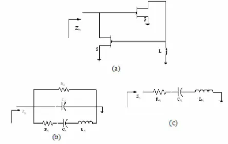
is not possible to realize a perfect match over a continuous band of frequencies by means of purely reactive (linear, passive losses) network. It is important that selected component for optimize the matching level and maximize the return loss level. In practice this resonant load can be realized by negative capacitor segments connected to an appropriate point of the patch antenna as shown in Figure 1. (a) l
i
f
- W r — l e -—VA If-V v \ 1( r^T^ F. C L X (C) (b)Figure 1 (a) Principle scheme of the negative capacitance circuit (b) Equivalent circuit of the negative capacitance circuit (c) Simplified equivalent circuit of the negative capacitance circuit
In principle, the radiation pattern of an antenna can be modified by variation of the current distribution on the antenna elements. The variation in the current distribution can be achieved by the incorporating one or more active loaded components into the antenna elements.
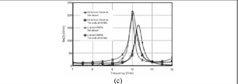
Theoretical analysis has been done by using multiport network model which is placed 10 ports peripheral of the patch antenna. The Multiport Network Model (MNM) for analyzing the MSA is an extension of the cavity model. In this model, the interior region and the exterior region are modeled separately [1]. The impedance matrix and the radiation conductance network are then combined by the segmentation method to obtain input impedance of the RMSA as shown in Figure 2 (a). Variation of the real part of the reference
and active loaded antenna impedances are shown in Figure 2 (c). It is clearly seen that the theoretical and simulation results are in well agreement.
The elements of the Z-matrix are derived from the Green functions as
Zj
= WWW IF
G (, Y'
xj ,Y
) d s J ( 5 )" i " j W Wj
where (xij,yij) denote the locations of the two ports of widths W, Wj,
respectively. Green's function G is usually a doubly infinite summation with terms corresponding to various modes of the planar resonator with magnetic walls. The segmentation method is then used to find the overall impedance matrix. Ë E CO ' y PÖ13 M n i « M PmW I ß «V(5 Port2 • t * Wi? .V.5 W Kl Pcn1 j jJ WV1 I m m Chip Resistor Point Nag ati va j Capacitance - r (a)
« E T *
TViffiUfüt •WTENMA Lisan) İ I I 1H
I a (b)Figure 2 (a) Original circuit configuration; (er = 3.0, h = 0.51 mm, L (length) =2 mm, ground
plane size=
40mm
x40mm
, R = 1 Q, (x1t y1) = (5.5, 0.5 mm), (x3, y3) = (0, 4 mm), and (x2,y2) = (3, 5.5 mm). (b) Equivalent circuit of the compensated patch antenna with negative
capacitance (c) Variation of the real part of the reference and active loaded antenna impedances with MNM
The total radiation is computed using the superposition of the far field radiated by each section. The far field pattern may be written in terms of voltages at the various elements.
N
F
o,=Y
V
(
i
)
W
(
i
)
{ 0 0)+«(i )}F ( M i = 1 whereSin
F
t(e,q>) =
-kW( i)
Cos(0)
kWOlccs (of
Sin (0)
(6) (7)Y
0(i) = X
0Sin (6) Cos (<p) + Y
0(i) Cos (0) (8)
and N is the number of ports, X0 (i), Y0 (i) specifies the location of the i-th magnetic current element, and W ( i ) is the width of the element.
3. PROPOSED ACTIVE COMPENSATED ANTENNA
NEGATIVE-CAPACITOR AND
CHIP-RESISTOR-LOADED RMSA
The rectangular microstrip patch antenna has been designed as a reference antenna. The 50 Q input impedance of the antenna is obtained
through proper choice of substrate thickness and the antenna dimensions. TLYA-5CH200 which has a relative permittivity of 3.20 and a thickness of 0.78 m m defined by the manufacture firm Taconic has been used as a substrate material. A simple rectangular microstrip patch antenna (RMSA) operating at 10.5 GHz has been utilized as a reference antenna. Substrate material specifications are summarized in Table 1.
Tablel. Board Specifications
Board Material Taconics, TLYA-5CH200
Substrate thickness 0.78 mm
Substrate dielectric constant 3.20 +/-0.02 Substrate dissipation factor 0.0009
Copper cladding thickness 0.018 mm (1/2 oz)
In this section the design sample of a rectangular patch antenna integrated with a negative capacitor is first discussed. When the negative capacitor circuit is connected to the rectangular microstrip patch antenna, the resulting equivalent circuit of the compensated system can be obtained as shown in Figure 2 (b). The patch dimensions of width W=16 mm and length L=9 mm have been selected along with the ground plane dimensions of 50x50mm. For these physical dimensions, the designed antenna operates at 10.55 GHz, with |S11| of -18 dB at the resonant frequency.
Proposed active compensation circuit consisting of negative capacitance has been analyzed. This circuit [8, 9] is based on a negative impedance converter, designed with two same type common-source transistors and loaded with an inductor as shown in Figure. 1(a). The negative capacitance circuit designed using the Fujitsu FSX017X GaAs FET having Cgs = 0.64 pF, gm = 54
mS, Cgd = 0.023 pF, Cd, = 0.096 pF, R, = 4.8 Q, Rs = 1.3 Q, Rd, = 538 Q in
operating condition VDS = 8 V, IDS = 35 mA .
When the influence of the parallel elements is negligible in Figure 1(b), the simplified equivalent circuit can be modeled as a series RLC circuit as shown in Figure 1(c).
The total input impedance ZN is then
7 1
1
i C sZn = 2R L — Y - J T . (9)
gm ds J g m gm
Two same type of FETs with identical transconductance (gm1 = gm2=gm) and
gate-source capacitance parameters (Cgs1= Cgs2=Cgs) are chosen and the
capacitance and inductance values in the equivalent RLC circuit can be represented as
r
N=
-gmR
6mf m ds lvdC
L n = —g t (10) g m CN = -g
m2 LThe element values in the equivalent circuit can be estimated as RN =-0.6374 Q , Ln=-0.219 nH, CN=-277.78 L pF for the Fujitsu FSX017X GaAs FETs.
Second port -loading port- was selected near the non radiating edge and opposite the feeding port on the patch geometry. When the negative capacitor circuit is connected to the output of the antenna, the resulting equivalent circuit of the compensated system can be obtained as shown in Figure 2 (b). The proposed antennas have been considered to be transmitter antennas. Active FETs have been placed in the transmitter state particularly with negative capacitor case. Loaded rectangular microstrip antenna (RMSA) as shown in Figure 1 yields high broadside radiation pattern in impedance bandwidth.
4. COMPARISON OF THE RESULTS
There are some classical techniques for the increasing the matching level and radiation pattern such as double stub, in according to feed point, aperture coupled R M S A [6]. These techniques were examined for comparison the proposed new loading configurations. These antennas are shown in Figure 3. The corresponding resonant frequency fr and the antenna gains for
different geometries are listed in Table 2.
Double stub matching method basically works to overcome the matching problem (in Fig 3.(c)). With an impedance matching double stub connected to the feed line increased matching level was achieved and its dimensions are W=16 m m and L=9 mm. W1=1.8 mm, L1=6.25 mm, W2=1.8
mm, Lstub1=7.5 mm, W3=1.8 m m Lstub2=11 mm, L2=10 mm, L3=10 mm. The results for the double stub technique are listed in Table 2. The single stub matching method basically works to overcome the fundamental bandwidth limitation.
Figure 3 Different geometry of the RMSA (a) Thick RMSA (S,=3.2, H=1.2 mm)
W
XL
=16 X 9 mm (b) Feed-point RMSA (H=0.78 mm, O=3.2,
tan(S)
= 0.0010 ) (c) Microstrip line feed RMSA (with double stub) (H=0.78 mm, S,=3.2 :TLC-32) (d) Geometry of aperture couple RMSA W X L = 1 6 X 9mm, stub length= 17mm,Sra =
1,tan
(Sa) = 0.0 (Foam), d
a=2 mm,S
rb =3.2,tan
(S
b) = 0.0009, Db=0.78
mm.
Table 2 Performance comparison for different techniques
Zin at fr (Ohm) Sıı (dB) (GHz) fr HPBW Beamwidth Computed Gain (dB) Reference Antenna 45.565+7.57j -18 10.55 76.6o 6.608
Microstrip Line Feed RMSA (with double stub) 57.423+6.412j -46.55 10.203 55.4° 7.608 Active Antenna (with negative capacitance) 42.363+10.13j 17.22F 10.55 77.7o 9.273 Matched-RMSA (Feed -Point) 47.765+0.006j -32.32 10.6 77.3o 4.338 Aperture-Coupled RMSA 41.519+3.389j -44.94 10.197 23.8o 8.55
For the evaluation and comparison purpose, the stub matching technique has been also applied to the reference patch antenna. An impedance matching stub connected to the feed line of the reference microstrip patch antenna is depicted in Figure 3 (b). The reference antenna, the stub matched antenna, and the active compensated antennas have been simulated. The results for the antenna impedances, bandwidth, return loss and the gain parameters have been evaluated using simulation data. The obtained antenna performances are also listed in Table 2.
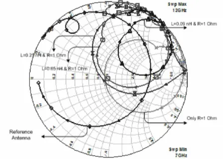
When the low chip resistor is added to the antenna as a loading, the antenna efficiency is decreasing. A single chip resistor loaded RMSA gives broadband operation with broadside radiation. However, Negative-Capacitor and Chip-Resistor-Loaded RMSA gives high gain broadside operation. Figure 2 (a) and (b) shows, respectively, the geometries of the original broadband microstrip antenna with an integrated reactive loading and proposed design with an additional loading of a resistance. The simulated results of the input impedance variations versus frequency are shown in Figure 4 for the reference and different loaded antenna configurations. When the loading position is
considered or the other loading techniques are used with the negative capacitor, better results in terms of matching level or co-polarization radiation levels are obtained. Figure 5 presents the simulated results of the return loss for both of original broadband rectangular microstrip antenna and the proposed design with active negative capacitance and chip resistor loading.
iwp Max 123 Hi t L-0.09jïH £ R=1 Otıırı IK St * Only R=1 Ctnn iwp Mln 7GHI
Figure 4 Input Impedance characteristics of the reference and loaded antennas versus frequency
10r -30 -40 -50 •g-L-o.tia nH i K-' unr. -H-l =0Jt rH i R=* or™ -I-1 -0.7H IW A R-- ClIWi ->.rı-ı 9 10 Fraqusncy (GHz)
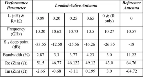
The reference and the loaded-active antenna performance are listed Table 3 for the different loading values. It is clearly seen that the Sn deep point and the resonant frequency can be adjusted with negative capacitance effect. The simulation results are summarized in Table 3 for the return loss and the radiation pattern parameters for various configurations.
Table 3 Performance comparison for the reference and the loaded-active (compact) antenna
Performance
Parameter Loaded-Active Antenna
Reference Antenna L (nH) & R = 1 Q 0.09 0.20 0.25 0.65 0 & (R only) 0 Frequency (GHz) 10.20 10.62 10.73 10.5 10.27 10.57 S11 deep point (dB) -33.55 -42.58 -25.56 -46.26 -26.35 -18 Bandwidth (%) 2.87 3.3 3.77 4.23 3.0 11.22 Re (Zin) (Q) 51.5 46.77 46.122 49.12 43.0 64.76 Im (Zin) (Q) -2.66 -0.68 -3.11 0.199 3.0 -64.72
The obtained return loss of the antenna with a reactive loaded in Figure 5, determined by return loss, is as large as -42 dB, which is about 2.3 times that of the original antenna. It is found that the enhancement in return loss level is obtained.
The antennas studied are all with a ground-plane size
of50mm
x50mm
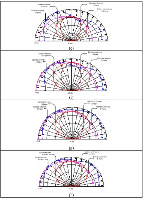
. Several proposed loaded antennas have been studied. Radiations patterns were also simulated for all the loaded configurations. Patterns quite typical of a more usual unloaded microstrip antenna were found with E-plane beam widths in the 85-95° range and the H-plane beam widths of 65-750. The radiation patterns were quite stable. It is observed that the component of the broadside radiation is increased for reactive loading case for H plane (y-z plane) and E plane (x-z plane) as shown in Figure 6.Figure 6 Simulated E plane and H plane radiation patterns for proposed loaded antenna and reference antenna (a) Antenna B1: Port 1= input port, Port 4= 1 Q, Port 3= Negative C (b) Antenna B2: Port 1 input port, Port 4 1 Q, Port 5Negative C (c) Port 1 input port, Port 4 1 Q, Port 2 Negative C (d) Port 1 input port, Port 3 1 Q, Port 5 Negative C (e) Port 1 input port, Port 2 1 Q, Port 5 and Port 4 Negative C (f) Port 1 input port, Port 3 1 Q, Port 5 and Port 4 Negative C (g)
Port 1 input port, Port 2 Negative C (h) Port 1 input port, Port 4 Negative C f=10.5 GHz RMSA Ground plane dimension; 4 0 X 4 0 X 0 . 5 2 mm & Er= 2.52.
At operating frequencies within the antenna bandwidth, the radiation patterns and antenna gain have been simulated to confirm the usefulness of the proposed antenna. When the negative capacitance is used as a reactive load, maximum gain of 9.273 dBi has been obtained with a small amount of shift in the resonant frequency .The E and H plane patterns have been investigated for the resonance frequencies in impedance bandwidth with respect to -20 dB. Best results have been obtained with the compensated active antenna in terms of Sn and radiation pattern.
Especially, good gain and beam shape results have been obtained in negative capacitive loading condition in E-plane pattern which is near the resonance frequency and there are shown in Figures 6-7. The maximum of the radiation pattern is in the broadside direction. The resonance frequency of the negative capacitance loaded RMSA is 10.5 GHz. With the proposed antenna design, the antenna gain can be large as about 2.5 times that of an antenna without reactive loading. The E-plane pattern has been dramatically improved for the active loading antenna. Note that the radiation power is normalized in broadside direction. The relatively large peak in the pattern of the reference patch has been obtained near the 0o. The asymmetry probably occurs due to the surface wave effects. However, different values for the specified parameters ( by changing the loaded values) may result in a better design in terms of radiation pattern.
5. CONCLUSIONS
A pattern synthesis method using a loaded network design for an antenna has been presented in this paper. High gain can be achieved using a single almost rectangular microstrip radiator reactively loaded with active negative capacitor. A single-feed broadband microstrip antenna with embedded reactive loading has been implemented. The simulated results of these configurations using commercially M o M based Microwave Office software followed by theoretical verifications are presented in this paper. The simulation results show that the compensation network with the negative capacitor can improve the return loss level from -18 dB to -42.58 dB. With a utilizing the negative capacitor and chip resistor loading as the loading circuit, antenna gain has been increased to 9.2 dB and the best radiation pattern in (E and H planes) has been obtained. These pattern shapes are similar to the reference antenna but results show that the radiation patterns of the active antenna with reactive loading case is significantly improved compared to conventional stub matching technique. The simulated results have demonstrated that one can control the input impedance and pattern, by appropriately varying the location of reactive loads.
REFERENCES
1. Benalla, A., & Gupta, C.; Multiport network model and transmission characteristics of two-port rectangular microstrip patch antennas, IEEE Trans. Antennas and Propagation, 36 (1998), 1337-1342.
2. Chair, R., Luk, K.M., and Lee, K.F.; Miniature multiplayer shorted patch antenna. Electron. Lett. 36 (2000), 3-4.
3. Chen, H.M.; Dual-frequency-microstrip antenna with embedded reactive loading. Microwave and Optical Technology Letters, 23 (1999), 186-188. 4. Elsdon, M. and Qin, Y.; Dual-frequency planar-fed microstrip patch
antenna, Microwave and Optical Technology Letter, 48 (2006), 1053-1054.
5. Fang, S.T., Chiou, T.W. and Wong, K.L.; Broadband equilateral-triangular microstrip antenna with asymmetric bent slots and integrated reactive loading, Microwave and Optical Technology Letters, 23 (1999), 149-151.
6. Garg, R., Bahartia, P., and Ittipiboon, A.; Microstrip antenna design handbook., Artech House. Boston.London, (2001).
7. Hsieh, G. B.; Dual-frequency rectangular microstrip antenna with an inserted integrated reactive loading, Microwave and Optical Technology Letters, 32 (2002), 219-221.
8. Koley, S., and Gautier, J.L.; Using a negative capacitance to increase the tuning range of a varactor diode in MMIC technology, IEEE Trans. On Microwave Theory and Techniques, 49 (2001), 2425-2430.
9. Mingo J., A. Valdovinos, Crepo, A. and Garcia, P.; An RF electronically controlled impedance tuning network design and its application to an antenna input impedance automatic matching system, IEEE Trans. on Microwave Theory and Tech. 52 (2004), 489-492.
10. Wong, K.L. and Jan, J.Y.; Broadband circular microstrip antenna with embedded reactive loading, Electron. Lett. 34 (1998), 1804-1805.
11. Yun, W. and Yoon, Y.; A wide-band aperture coupled microstrip array antenna using inverted feeding structures, IEEE Antennas and Propagat. 53 (2005), 861-862.