Graphene Nanoplatelets Embedded in HfO2 for MOS Memory
N. El-Ataba, B. B. Turgutb, A. K. Okyayb,c,d, A. Nayfeha
a
Institute Center for Microsystems – iMicro, EECS, Masdar Institute of Science and Technology Abu Dhabi, United Arab Emirates
b
UNAM-National Nanotechnology Research Center, Bilkent University, 06800 Ankara, Turkey
c
Institute of Materials Science and Nanotechnology, Bilkent University, 06800 Ankara, Turkey
d
Department of Electrical and Electronics Engineering, Bilkent University, 06800 Ankara, Turkey
In this work, a MOS memory with graphene nanoplatelets charge trapping layer and a double layer high-қ Al2O3/HfO2 tunnel oxide
is demonstrated. Using C-Vgate measurements, the memory showed
a large memory window at low program/erase voltages. The analysis of the C-V characteristics shows that electrons are being stored in the graphene-nanoplatelets during the program operation. In addition, the retention characteristic of the memory is studied by plotting the hysteresis measurement vs. time. The measured excellent retention characteristic (28.8% charge loss in 10 years) is due to the large electron affinity of the graphene. The analysis of the plot of the energy band diagram of the MOS structure further proves its good retention characteristic. Finally, the results show that such graphene nanoplatelets are promising in future low-power non-volatile memory devices.
Introduction
Recently, two-dimensional graphene has attracted great efforts and research due to its unique characteristics such as large work-function, high carrier mobility, thermal conductivity, and optical transparency (1-3). These outstanding properties enabled promising graphene-based electronics, filtration, photovoltaics and energy storage devices (4-7). However, the use of graphene in non-volatile memory devices hasn’t been studied extensively. In this work, the effect of using Quattro-layer graphene-nanoplatelets as a charge trapping layer in non-volatile MOS memory devices with double layer Al2O3/HfO2 tunnel oxide is investigated. The memory performance is studied by
conducting high frequency C-V measurements, charge retention measurement, and analysis of the energy band diagram of the memory structure.
Experimental
The fabrication of the memory cells is conducted as follows: first a 4-nm-thick tunnel oxide Al2O3 is deposited at 250°C in Cambridge Nanotech Savannah-100 atomic layer
deposition (ALD) system on an n+-type (111) (Antimony doped, 15-20 mΩ-cm) Si wafer. Next, 1-nm-thick HfO2 is deposited by Plasma Assisted ALD at 195°C in an Oxford
graphene nanoplatelets solution with 0.05 mg/ml concentration are drop casted slowly using pipettes. A 1-nm-thick HfO2 is again deposited by plasma assisted ALD at 195°C
followed by an 8-nm-thick Al2O3 blocking oxide deposited by ALD at 250°C. Finally,
the gate contacts are created by e-beam evaporating a 400-nm-thick Al layer using a shadow mask with 10 μm feature size. An illustrative cross-section of the fabricated memory is shown in Figure 1.
Figure 1: Schematic cross-section of the fabricated charge trapping memory cell with graphene nanoplatelets.
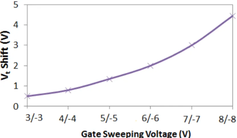
In order to analyze the effect of embedding graphene nanoplatelets in the MOS memory and to quantify the stored charge at different gate voltages, high frequency (1 MHz) C-Vgate measurements are conducted using an Agilent B1505A Semiconductor Device Parameter Analyzer to measure the programmed and erased C-V characteristics of the fabricated memory devices as depicted in Figure 2. The memory cells showed a 1.35 V threshold voltage (Vt) shift upon sweeping the gate voltage from -5 V forward to
5 V then backwards. At -7/7 V gate sweeping voltage, more charging is observed through the higher 3 V Vt shift as shown in Figure 3. The results show that the memory is being
programmed by storing electrons in the graphene nanoplatelets as shown by the shift of the programmed state in the positive direction at higher gate sweeping voltages (8-10). The observed pure electrons storage is expected to increase the program/erase operations speeds with respect to memory devices where both electrons and holes are stored due to the larger mass of holes and larger valence band offsets.
Figure 2: Measured hysteresis behavior using the C-Vgate characteristic showing a 3 V Vt shift at 7/-7 V gate sweeping voltage.
At 7/-7 V gate sweeping voltage and with a measured 3 V Vt shift, the charge
trapping density in the graphene nanoplatelets is calculated (11-13) and found to be 1.54 ×1013 cm-3.
Figure 3: Measured threshold voltage shift using the C-Vgate characteristic at different gate sweeping voltage.
Using the reported material properties of Al2O3, HfO2, and graphene, the energy band
diagram of the memory is constructed as shown in Figure 4 (14-31). The conduction band offset between Si and tunnel oxide is smaller than the valence band offset (ΔEC = 2.44 eV
< ΔEV = 3.24 eV), thus the electrons tunneling probability is expected to be much higher
than holes tunneling probability which confirms the observed electrons storage. In addition, due to the large work-function of graphene, a deep quantum well is formed where electrons can be stored. In fact, the conduction band offset between charge trapping layer and tunnel oxide is very large (ΔEC = 2.99 eV) which exponentially
reduces the leakage of stored electrons in the graphene nanoplatelets as expressed in Einstein’s quantum tunneling equation (11-12). Moreover, the addition of the high-dielectric constant (қ=20) HfO2 layer is expected to further reduce the leakage of stored
charges.
Figure 4: Energy band diagram of the fabricated MOS memory with graphene nanoplatelets.
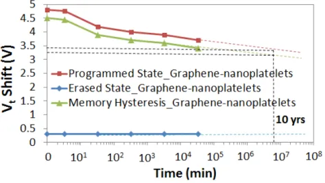
Furthermore, the retention of the memory cells is characterized by first programming/erasing the memory at 8/-8 V and observing the change in Vt shift in time
as shown in Figure 5. The figure shows that 28.8% of the initial charge is lost in 10 years and a memory hysteresis of ~3.3 V is shown at 10 years. This good retention
characteristic with graphene nanoplatelets is due to the large electron affinity of graphene (4.6 eV) which increases the conduction band offset between charge-storage layer and tunnel oxide, and therefore exponentially reduces the back tunneling of electrons.
Figure 5: Retention characteristic of the MOS memory with graphene nanoplatelets
Conclusion
In conclusion, a MOS memory device with graphene nanoplatelets and double layer Al2O3/HfO2 tunnel oxide is demonstrated. The results show that graphene nanoplatelets
provide a large memory window at low operating voltages in addition to an excellent retention characteristic which is due to the large conduction band offset between charge storage layer and Al2O3. The results highlight that such memory structures have potential
in next-generation low power non-volatile-memory devices.
Acknowledgments
This work was supported by Masdar Institute of Science and Technology, and TUBITAK Grants 111A015, 112M004, 112E052 and 113M815. A.K.O. acknowledges support from the Turkish Academy of Sciences Distinguished Young Scientist Award (TUBA GEBIP).
References
1. K. S. Novoselov et al., Science 306, 666 (2004) 2. F. Schwierz, Nat. Nanotechnol. 5, 487–496 (2010) 3. S. Wang et al., Appl. Phys. Lett. 96, 143109 (2010) 4. J. S. Lee et al., Nat. Nanotechnol. 2, 790 – 795 (2007)
5. N. El-Atab, F. Cimen, S. Alkis, A. K. Okyay, and A. Nayfeh, Appl. Phys. Lett.
105, 033102 (2014)
6. S. Bertolazzi, D. Krasnozhon, A. Kis, ACS Nano 7, 3246–3252 (2013) 7. Y. J. Yu et al., Nano Lett. 9, 3430–3434 (2009)
8. O. M. Nayfeh, Ph.D dissertation, EECS, MIT, Cambridge, MA (2009)
9. N. El-Atab, A. Ozcan, S. Alkis, A. K. Okyay, and A. Nayfeh, Appl. Phys. Lett.
10. N. El-Atab, A. Rizk, A. K. Okyay, A. Nayfeh, AIP Advances 3, 112116 (2013) 11. D. J. Griffiths, Introduction to Quantum Mechanics, Second ed., Prentice Hall,
Upper Saddle River, New Jersey (2004)
12. S. M. Sze and K. K. Ng, Physics of Semiconductor Devices, Third ed., JOHN WILEY & SONS, Hoboken, New Jersey (2007)
13. N. El-Atab, A. Ozcan, S. Alkis, A. K. Okyay, and A. Nayfeh, Phys. Status Solidi RRL 8, 629 (2014) DOI: 10.1002/pssr.201409157
14. S. S. Datta, D. R. Strachan, E. J. Mele, A. T. C. Johnson, Nano Lett. 9, 7–11 (2009).
15. K. S. Novoselov et al., Nature 438, 197 (2005)
16. C. M. Tanner, Y. C. Perng, C. Frewin, S. E. Saddow, J. P. Chang, Appl. Phys. Lett. 91, 203510 (2007)
17. H. He, R. Orlando, M. A. Blanco, R. Pandey, E. Amzallag, I. Baraille, M. Rérat, Phys. Rev. B 79, 195123 (2006)
18. M. F. Li et al. 7th International Conference on Solid-State and Integrated Circuits Technology, Proceedings. 1, 366 (2004)
19. N. El-Atab, A. Rizk, B. Tekcan, S. Alkis, A. K. Okyay, and A. Nayfeh, Phys. Status Solidi A 212 (2015) / DOI 10.1002/pssa.201431802
20. Y. S. Lin, R. Puthenkovilakam, J. P. and Chang, Appl. Phys. Lett. 81, 2041 (2002) 21. N. El-Atab, A. Ozcan, S. Alkis, A. K. Okyay, and A. Nayfeh, 14th IEEE
International Conference on Nanotechnology p. 505-509. DOI:
10.1109/NANO.2014.6968168 (2014)
22. A. Nayfeh, A. K. Okyay, N. El-Atab, A. Ozcan, S. Alkis,Invited, 226th ECS Meeting Abstract no. 46, p. 2143-2143 (2014)
23. A. Nayfeh, A. K. Okyay, N. El-Atab, F. Cimen, S. Alkis, Invited, 226th ECS Meeting Abstract no. 37, p. 1879-1879 (2014)
24. S. J. Choi, J. H. Han, S. Kim, D. I. Moon, M. Jang, and Y. K. Choi, 2010 Symposium on VLSI Technology Digest of Technical Papers, 111-112, (2010) 25. X. Wang, D. L. Kwong, IEEE Trans. Electron Devices 53, 78 (2006)
26. N. El-Atab et al., AIP Advances 3, 102119 (2013) 27. S. D. Ganichev, Physical Review 61, 10361 (2000)
28. H. X. Wang, J. Liu, W. Bai, and D. L. Kwong, IEEE Trans. Electron Devices 51, 597–602 (2004)
29. N. El-Atab et al. Appl. Phys. Lett. 104, 253106 (2014) 30. G. Mazzeo et al. Appl. Phys. Lett 96, 213501 (2010)
31. N. El-Atab et al. Nanoscale Res. Lett. 10, 248 (2015). DOI:10.1186/s11671-015-0957-5