: 1
Α
, Sualp Aras
Α >> Dept. of Computer Engr., Dogus University,
Α
Department of Electronics and Communication Engineering Maslak 80626, Istanbul , Turkey
ABSTRACT
The implementation of a perceptron that can classify data separable by two parallel hyper-planes or equivalently of a Single-Level TL-XOR gate is proposed using 10 MOS transistors and 2 capacitors. The functional sub-block decomposition of the Perceptron with two separating hyper-planes, its CMOS implementation explaining the operation of each sub-block and simulation results, obtained using the SpectreS simulator and AMS 0.8µm CMOS double-poly double-metal technology parameters are presented. A brief outline of the two level CTL realization and its comparison with the new implementation are given as far as their transistor count, programmability and total delay are concerned.
Key Words : Perceptron, Neural Networks, Threshold Logic, XOR Gate
I. INTRODUCTION
One of the simplest Neural Network topologies is the Perceptron shown in Figure 1.a, introduced in [1] and widely investigated in the literature. An Internet
search for the word "Perceptron" gave approximately 10.000 results. A Single-Cell-Perceptron (SCP) can be viewed as an Analog to Digital Converter classifying data according to
Θ
<
Θ
>
=
∑
∑
= = i n 1 i i i i n 1 i i ix
w
for
0
x
w
for
1
y
(1)
X2 X1 W1X1 + W2X2 = 0 X2 X1 X1 X2 Xn Θi y Perceptron Fig.1.an n-input perceptron 1.b Linearly separable data 1.c Not linearly separable dataObviously the kind of data that the perceptron can classify is of the type that is Separable by a Hyper-Plane (a line if n = 2) as shown in Figure 1.b and not of the type as shown in Figure 1.c.. Among the data unclassified by the perceptron the most famous one is the one that belongs to the XOR gate which has data
A very closely related concept to the perceptron is the Threshold Logic (TL) where a perceptron-like configuration that acts as an XOR gate is given with a two level realization as shown in Figure 2 using 2 TL-AND and a standard OR gates (several variants are available [2]).
T SAYI
Devrim Yılmaz Aksın
, İzzet Cem Göknar
ETA ASIC Design Center and İstanbul Technical University
REALIZATION AND EXTENSIONS OF USER PROGRAMMABLE,
SINGLE-LEVEL, DOUBLE-THRESHOLD GENERALIZED
TL - AND
TL - AND
ORX
1X
2X
2X
1Y
Figure 2. Two Level XOR Gate
In this paper a perceptron that can classify data separable by two parallel hyper-planes (as shown in Figure 1.c) or equivalently a Single-Level TL-XOR gate is implemented using 10 MOS transistors and 2 capacitors.
In section II of this paper, the functional sub-block decomposition of the Perceptron with two separating hyper-planes, in section III, its CMOS implementation explaining the operation of each sub-block implementation are presented. Section IV contains a brief outline of the two level CTL realization and its comparison with the new implementation as far as their transistor count and total delay are concerned.
Section V is the concluding one also containing further research issues.
II. FUNCTIONAL DESCRIPTION OF THE CIRCUIT
Functionally the circuit can be viewed as consisting of three sub-blocks. These are the adder that sums up the weighted input signals, the threshold circuit that produces an output signal if the sum is within the user programmed thresholds and the comparator that produces proper logic-level at the output of the circuit determined by the output of the threshold circuit. The functional block diagram of the circuit is shown in Figure 3.
Figure 3. Functional block diagram of the double threshold XOR gate
The output signals, O1, O2 and O3, are defined as follows
=
=
<
<
=
+
=
else
High
Logic
0
O
Low
Logic
O
else
0
T
O
T
)
O
(
f
O
I
K
I
K
O
2 3 2 1 1 1 2 2 2 1 1 1(2)
III. CMOS IMPLEMENTATION
The CMOS implementation of the XOR gate is given in Figure 4.
Figure 4. CMOS implementation of the double threshold XOR gate
.
The bulk terminals of all NMOS transistors are connected to the ground and the bulk terminal of all PMOS transistors, except M1, to the positive power supply.
III.1 THE ADDER
The adder consists of the input capacitors C1
and C2, switch transistor M3 and input capacitor of the
transistors M1 and M2. The small signal equivalent circuit of the adder is illustrated in Figure 5.
Figure 5. Small signal equivalent of the adder
Here CX represents the input capacitance of the
transistors M1 and M2.
Operation of the circuit consists of two phases. During the reset phase, input voltages, V1 and V2, are set to
the ground voltage level and switch transistor M3 connects VB terminal to the internal node, O1. For
these biasing conditions, the charge accumulated at node O1 can be expressed as follows
B 2 B 1 B X RP
C
V
C
V
C
V
Q
=
+
+
(3)where QRP denotes the amount of charge at O1 in the
reset phase.
During the operation phase, the switch is open and the node O1 becomes floating; and the inputs are applied
to the circuit. In this phase, the charge of O1, which is
equal to the amount of charge of the reset phase, can be expressed as follows
(
O1 1) (
2 O2 2)
1 1 O X OPC
V
C
V
V
C
V
V
Q
=
+
−
+
−
(4)where QOP denotes the amount of charge at O1 in the
operation phase. Since the charge is conserved at this node during operation, the voltage level of O1 can be
obtained by equating QRP to QOP. Thus
2 2 1 1 B 1 O
V
C
C
C
C
V
C
C
C
C
V
V
+
+
+
+
+
+
=
(5)This is exactly the expected equality for the adder block with an offset term, VB, that can be chosen
arbitrarily.
In the operation phase, the input capacitance, represented by CX, varies with the node voltage VO1
due to the operation region changes of the t ransistors M1 and M2. But the effect of CX can be neglected by
choosing the input capacitors, C1 and C2, sufficiently large.
The phase cycle is determined with respect to the order of magnitude of the leakage current of the node O1. Obviously, if the leakage does not exist, the circuit
does not need another reset phase. The magnitude of the leakage current is strongly dependent on the ambient temperature. Therefore, this effect must be taken into account when determining the cycle frequency. Evidently, increasing the total capacitance at the node O1 will result in decreasing cycle
frequency.
The previous analysis is based on the assumption that during the operation phase, the node O1 is floating. To
assure the validity of the assumption, the reverse biased P-N drain-bulk junction of the switch transistor M3 must never be forward biased. Therefore, the coefficients determined by the capacitors, input signal range and bias voltage VB must be consistent with this
condition.
III.2 THE THRESHOLD CIRCUIT
To provide the double threshold feature a simple CMOS inverter's VIN-IDD characteristic, as given in
Figure 6, is exploited. Inverter's threshold voltage, expressed in (6), and the voltage VB are used to shift the current curve to the desired location.
(
)
2 1 01 T DD 2 1 2 TO TH KP KP 1 V V KP KP V V + + + = (6)where VT0i and KPi are the threshold voltages and the
transconductance parameter of the ith transistor, respectively. In order to eliminate the body effect of the transistor M1, which influences its threshold voltage VT01, this transistor is realized in a separate
well permitting to connect its bulk terminal to its source terminal. The normalized sensitivity of the threshold voltage, VTH, to positive supply voltage
VDD, which can be expressed as
(
DD T01)
2 1 02 T DD 2 1 TH DD DD TH V V KP KP V V KP KP V V V V + + = δ δ (7)is very high. Therefore, the source terminal's voltage of the transistor M1 must be very stable. Variation of
the inverter current for different bias voltage VB is
plotted in Figure 6.
Figure 6. Variation of the Inverter Current For Different Bias Voltage VB
III.3 THE COMPARATOR
The Comparator, which is the last saub-circuit, extracts the inverter current while keeping its input voltage constant and produces a logic level in correlation with the extracted current exceeding a certain limit or not.
In order to understand easily how the circuit operates, it will be first assumed that the drain terminal of the transistor M6 is directly connected to the ground potential and how the transistor M7 functions will be explained.
The biasing voltage Vbias1 of the transistor M4 is so
chosen that the drain current ID(M4) is always greater
than the input current IO2. Due to the Kirchoff current
law, the difference current, which is equal to ID(M4)-IO2,
flows through the transistor M6, and this output current is used to obtain a logic level with transistor M7. The feedback-loop consisting of transistors M5, M6 and M8 is used to hold the input DC voltage level constant. The circuit formed by transistors M5 and M8 is a simple amplifier having negative gain, and the circuit formed by transistors M6 and M4 can be considered as a simple unity gain source-follower. Therefore, the feedback-loop helps to minimize the voltage change on node O2. The input DC voltage
level can be expressed as
5 ) 8 M ( D 05 T DD 2 O
KP
I
2
V
V
V
=
+
−
(8)Small signal input resistance of the comparator, which has an order of magnitude of 50 Ω, can be approximated as 5 6 5 ) 2 O ( IN
gm
gm
8
gds
gds
r
=
+
(9)and it can be made even smaller by simply increasing the loop gain [3].
Now the effect of transistor M7 will be explained. For this transistor, which operates as a current source, the biasing voltage Vbias2 is so chosen that its drain current
is smaller than the drain current of the transistor M4. With this simple modification, the comparator's new operation can be explained as follows
If the sum of the currents IO2 and ID(M7) is smaller than
the current ID(M4), the voltage of the node O2 starts to
increase, as does the input voltage of the inverter at the output, until the transistor M4 enters the linear operation region and decreases its drain current. The voltage variation on node O2 increases with the increase in the drain current difference of the transistors M4 and M7. Vice versa, the magnitude of the input current IO2, for inverting the output,
decreases with the increase in the drain current difference. This feature allows adjustment of the decision threshold. Variation of the decision region of the cell with different bias current is given in Figure 7.
Figure.7 Decision region of the cell for different current bias
If the sum of the currents is greater than ID(M4),
transistor M4 operates in saturation region. The feedback minimizes the input voltage change and, as there is no sufficient amount of current for transistor
decrease until this transistor enters the linear operation region. Obviously, the operation speed of the cell is a function of the current difference, ID(M4)-IO2-ID(M7).
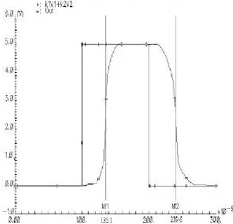
Therefore, increasing current threshold decreases operation speed. The response time of the XOR gate for ID(M4) equal to 55uA is plotted in Figure 8. TPLH
and TPHL of the gate are 35.1ns and 39.6ns,
respectively. Finally, the output voltage VO3 goes to
logic high as the input voltage of the inverter is decreased.
Figure 8. The response time of the XOR gate for ID(M4)=55Ua
As mentioned previously, input node voltage changes when transistor M4 enters the linear operation region. This situation causes the location of the thresholds of the Threshold circuit to vary during the operation. For applications where this is intolerable, the transistor M7 can be replaced by a current mirror and the comparison can be done with the next stage. This will guarantee a constant voltage level at node O2.
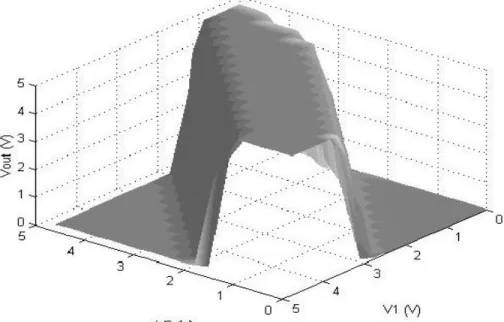
The transfer surface graph of the complete circuit is as shown in Figure.9
IV. PERFORMANCE COMPARISON
WITH TWO LEVEL CTL-CMOS XOR
GATE
An alternative realization of the XOR gate exploiting the CTL implementation technique proposed in [4,5] is used for performance and area comparisons. CTL implementation allows a two-level realization as shown in Figure 2 whereas proposed gate implementation resolves the XOR problem in single level. The CTL XOR gate consists of 32 minimum sized transistors and 6 capacitors whereas the proposed structure consists of 10 transistor and 2 capacitors.
Another advantage of the proposed XOR gate is its simple continuos time user programmable operation while the CTL implementation is mask programmable and suffers from the complex time scheme using two phase clock generation to satisfy the sampled -analog
behavior of this technique. The average response time of the single-level XOR gate is approximately 37ns while the CTL XOR gate has an average cycle time of approximately 10ns.
Figure.9 Transfer Surface of the XOR Gate
(a) (b)
Figure 10. Simulation results showing complex decision regions realization for 2-D input space.
V. FUTURE EXTENSIONS
In this paper, a circuit that separates the input space into two regions of which boundaries are determined by two programmable threshold, is presented. More complex classification abilities can be implemented using a “multi-threshold” variant of the proposed circuit that realizes programmable enclosed decision regions in the input space. The simulation results showing four and five enclosed decision region cases are given in Figure 10(a) and 10(b). Notice that the location and the enclosed area of any region can be individually programmed.
VI. CONCLUSION
The user and/or mask programmability features of the proposed cell were mentioned previously in section III. In summary, the decision region can be diagonally shifted in the input space with the aid of the bias voltage VB. Since bias voltage is applied only during
the reset phase, programming of a network consisting of multiple parallel processing cells having different decision regions can be carried out using single bias net and sequential resetting of the cells. Main advantage of this feature is the ease in constructing an adaptive network using a digital control block with DAC and RAM blocks. Additional programming
capability is also supplied by the bias of the transistor M4, which allows the tuning of the width of the decision region. Finally, the decision region can be rotated by selecting the ratio of the cell's input capacitors properly.
As a result, a single-level double-threshold generalised perceptron capable of evaluating the classical XOR function has been designed. The cell consists of only 10 transistors and 2 capacitors. Simulation results, obtained using the SpectreS simulator and AMS 0.8µm CMOS double-poly double-metal technology parameters, were presented in the previous sections.
The proposed circuit can easily be augmented to handle decision regions for more than two inputs and the design of a CMOS circuit with closed polyhedral decision regions is under investigation.
REFERENCES
1. Rosenblatt, F., "The perceptron: A probabilistic model for information storage and organisation in the brain." Psychological Review 65, 386-408, 1958.
2. Haykin, S., Neural Networks. A Comprehensive
Foundation, New York: Macmillan College
Publishing, 1994.
3. Aksýn,D.Y., A Programmable CMOS Analog Vector Quantizer Chip. MSc. Thesis, ÝTÜ, Aug 1999.
4. Özdemir, H. et al, "Capacitive threshold logic gate," IEEE J. of Solid State Circuits 31, 8, 1141-1150, Aug. 1996.
5. Leblebici, Y. et al, "Compact high-speed (31,5) parallel counter circuit based on capacitive threshold -logic gates," IEEE Journal of Solid-State Circuits 31, 8, 1177-1183, Aug 1996.