Adsorption of Group-IV Elements on Graphene,
Silicene, Germanene, Stanene: Dumbbell Formation
V. Ongun Özçelik,
∗,†,‡D. Kecik,
∗,†,‡E. Durgun,
∗,†,‡and S. Ciraci
∗,¶UNAM-National Nanotechnology Research Center, Bilkent University, 06800 Ankara, Turkey, Institute of Materials Science and Nanotechnology, Bilkent University, Ankara 06800, Turkey,
and Department of Physics, Bilkent University, Ankara 06800, Turkey
E-mail: [email protected]; [email protected]; [email protected]; [email protected]
Abstract
Silicene and germanene derivatives constructed from periodic dumbbell units play a crucial role in multilayers of these honeycomb structures. Using first-principles calculations based on density functional theory, here we investigate the dumbbell formation mechanisms and energetics of Group IV atoms adsorbed on graphene, silicene, germanene and stanene monolayer honeycomb structures. The stabilities of the binding structures are further confirmed by performing ab-initio molecular dynamics calculations at elevated temperatures, except for stanene which is subject to structural instability upon the adsorption of adatoms. Depending on the row number of the adatoms and substrates we find three types of binding structures, which lead to significant changes in the electronic, magnetic, and optical properties of substrates. In particular, Si, Ge and Sn adatoms adsorbed on silicene and germanene form dumbbell structures. Furthermore, dumbbell structures occur not only on single layer, monatomic honeycomb structures, but also on their compounds like SiC and SiGe. We show that the energy barrier to the migration of a dumbbell structure is low due to the concerted action of atoms. This renders dumbbells rather mobile on substrates to construct new single and multilayer Si and Ge phases.
Introduction
Recent theoretical and experimental studies have proven that silicon,1–5 germanium,6–9 compound semiconductors,6α -silica,10α -tin,11–14transition metal oxides and dichalcogenides15–18 can have stable, single layer honeycomb structures like graphene. However, in contrast to suspended graphene which can be easily exfoliated from 3D layered graphite; free-standing single layers of Si, Ge and Sn were not synthesized yet, since these elements do not exist as 3D layered bulk phase in nature. Therefore, it is a much accessible way (and the only possible way so far), to synthesize single layers of Si (i.e. silicene), Ge (i.e. germanene) and Sn (i.e. stanene) on suitable substrates like silver and gold. Under these circumstances, the
growth of stable multilayers of silicene was re-cently achieved.7,19,20 After the synthesis of thick layered silicene, the possibility of the layered bulk allotrope of silicon has been explored and sta-ble bulk phases of Si have been predicted, which show a layered character and display electronic and optical properties different from those of the well-known cubic diamond structure.21 These re-sults were further supported by the experimental data collected from multilayer silicene grown on Ag(111) substrate.7,19,20
Understanding the structure of layered silicene is of particular importance in a wide range of appli-cations from electronics design to Li-ion storage for batteries.22 Scanning tunneling microscopy (STM) measurements aiming at the understand-ing of the structure of multilayer silicene grown
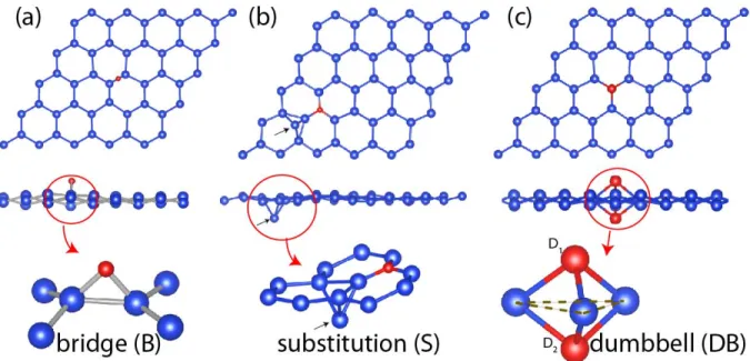
Figure 1: Side and top views of various types of equilibrium atomic structures, which occur when a Group IV ele-ment (C, Si, Ge and Sn) is adsorbed on the single layer honeycomb structure constructed from Group IV eleele-ments (graphene, silicene and germanene). (a) A Group IV adatom adsorbed at the bridge site, i.e. B-site. (b) Substitution of silicene or germanene host atoms by the carbon adatom, i.e. S-site. The small arrows indicate the host Si atom that is pushed down after the substitution of C adatom. (c) Dumbbell structure (DB) constructed by Si, Ge and Sn adatoms adsorbed on silicene and germanene. D1and D2are dumbbell atoms; D1is the adatom, D2is the host atom
pushed down by D1. Adatom and single-layer substrate atoms are described by red and blue balls, respectively.
on Ag(111) substrate7,19revealed that silicene lay-ers have a (√3 ×√3) supercell with honeycomb structure. Earlier, theoretical studies found that the adsorption of a Si adatom on silicene is exothermic and results in a dumbbell structure (DB), where the Si adatom attached to the top side on silicene pushes the host Si atom down to form a cage.23–26 Recently, silicene derivatives constructed from pe-riodic patterns of DB structures are found to be en-ergetically more favorable.27 Additionally, stack-ing of these DB based silicene derivatives repro-duced the structure data obtained from STM mea-surements of grown multilayers. These findings have pointed that the grown multilayer silicenes may, in fact, be constructed from the dumbbell based single layer phases of silicene.27 Further-more, our recent letter8 shows that stable DB structures can occur not only on silicene, but also on germanene. Then the important question re-mains to be answered is whether DB based single layer phases can be common to all Group IV ele-ments.
Motivated with the remarkable aspects of the DB structures, their insight on the layered allotropes and coverage depended phases revealed,8 in this
study we carried out an extensive analysis of the adsorption of the Group IV adatoms (C, Si, Ge and Sn) on the single layer honeycomb substrates con-structed from these atoms (i.e. graphene, silicene, germanene, and stanene) amounting to 16 possi-ble adatom+substrate combinations. Furthermore, we extended our analysis to include single-layers compounds, such as SiC and SiGe. The question of whether the DB structure is common to all of these systems has been our starting point. Im-portant findings of our study can be summarized as: (i) Three different types of equilibrium binding structures can occur when Group IV adatoms ad-sorb on graphene, silicene and germanene. These are specified as bridge bonding (B), substitutional (S), and dumbbell (DB). (ii) DB structure is not observed if the adatom or monatomic, single layer honeycomb substrate involves carbon atom. (iii) A structural instability is induced when one atom from Group IV elements is adsorbed on stanene, whereby the honeycomb structure is disrupted even at T=0 K. (iv) In silicene and germanene, C adatom substitutes host Si and Ge atoms. (v) Si, Ge and Sn form stable DB structures on silicene, as well as germanene with critical electronic,
mag-netic, and optical properties. (vi) In compound sin-gle layer honeycomb structure of silicon carbide, C adatom forms dumbbell structure; similar to Si and Ge adatoms adsorbed on single layer SiGe compound. (vii) We showed that the energy barrier for the migration of DBs is not high due to the con-certed process of atoms at close proximity. This situation renders DB structures of Si, Ge and Sn mobile on silicene and germanene and paves the way to grow new single layer phases having dif-ferent periodic patterns of the DBs. These phases, in turn, can offer alternatives to grow thin films or layered bulk structures and their compounds with diverse properties. (viii) Present results indicates that novel electronic, magnetic and optical proper-ties can be achieved through the periodic coverage of graphene, silicene and germanene by Group IV adatoms.
Method
Our predictions were obtained from first-principles pseudopotential calculations based on the spin-polarized density functional theory (DFT)28,29 within generalized gradient approx-imation (GGA) including van der Waals cor-rections.30 Projector-augmented wave potentials (PAW)31 were used and the exchange-correlation potential was approximated with Perdew-Burke-Ernzerhof (PBE) functional.32 Adsorption of sin-gle adatom on various sinsin-gle layer honeycomb structures was simulated by using periodically repeating supercell method in terms of 5×5 super-cells comprising 50 host atoms and one adatom. The Brillouin zone (BZ) was sampled according to the Monkhorst-Pack scheme, where the con-vergence in energy as a function of the number of k-points was tested. The k-point sampling of (21×21×1) was found to be suitable for the BZ corresponding to the primitive unit cells of substrates. For larger supercells this sampling has been scaled accordingly. For the case of the 5×5 cell used in this study, the k-point sampling was chosen as 5×5×1. Atomic positions were optimized using the conjugate gradient method, where the total energy and atomic forces were minimized. The energy convergence value be-tween two consecutive steps was chosen as 10−5
eV. A maximum force of 0.002 eV/Å was al-lowed on each atom. Numerical calculations were carried out using the VASP software.33 Since the band gaps are underestimated by standard-DFT methods, we also carried out calculations using the Heyd-Scuseria-Ernzerhof(HSE) hybrid func-tional,34,35 which is constructed by mixing 25 % of the Fock exchange with 75 % of the PBE exchange and 100 % of the PBE correlation en-ergy. For the optical properties computed at the random phase approximation (RPA) level,36 a (127×127×1) k-point grid and a total of 96 bands were undertaken for a proper description of the dielectric function.
The binding energy Eb, was calculated using
the expression Eb = ET[A] + ET[sub] − ET[A +
sub] in terms of the optimized total energies of adatom ET[A], of bare substrate (graphene,
sil-icene, etc.) ET[sub] and of adatom adsorbed on
substrate ET[A + sub], all calculated in the same
supercell. Positive values of Eb indicate that the
adsorption of the adatom is an exothermic process and is energetically favorable.
Further to conjugate gradient method, the stabil-ities of structures were tested by ab-initio molec-ular dynamic (MD) calculations performed at fi-nite temperatures. A Verlet algorithm was used to integrate Newton’s equations of motion with time steps of 2 f s. We carried out MD calculations at temperatures T = 200K, T = 400K, T = 600K, T = 800K and T = 1500K, each lasting 1ps and totaling to 5ps for each adatom+substrate system. To maintain the system in the desired constant temperature, the velocities of atoms were rescaled in each time step allowing a continuous increase or decrease of the kinetic energy.
Equilibrium Structures and
En-ergetics
Adsorption of Group IV atoms on single layer graphene, silicene, germanene, and stanene are studied in terms of periodically repeating super-cell method, where one adatom is adsorbed in each 5×5 supercell. Since the adatom-adatom coupling between the 5×5 supercells is minute, this system can be taken to mimic the single, isolated adatom and the local reconstruction thereof. The
equi-librium binding structures and corresponding lo-cal reconstruction of C, Si, Ge and Sn adatoms on graphene, silicene, germanene, and stanene sub-strates have been explored by placing the adatoms at various sites and optimizing the atomic struc-tures using conjugate gradient method. The op-timized binding structures, namely B, S and DB are schematically described in 1. Corresponding structural parameters, binding energy, magnetic and electronic structure are summarized in 1. All of Group IV adatoms on stanene give rise to mas-sive local reconstruction leading to the destruction of honeycomb structure in the 5×5 supercell. This structural instability occurring even in the course of structure optimization using conjugate gradi-ent method at T = 0K is critical, since it does not comprise artificial effects, like small unit cells enhancing stability etc. The instability followed by adatom adsorption implies that the single layer honeycomb structure of Sn is in a shallow mini-mum and is prone to structural deformations.
In particular, the carbon atom having electronic structure 1s22s22p6, behaves rather differently from the rest of the Group IV elements. For ex-ample, owing to relatively smaller C-C bond the π - π interaction stabilizes the planar structure of graphene attained by sp2 bonding. Whereas sin-gle layer honeycomb structures of silicene, ger-manene and stanene are stabilized through buck-ling of atoms ensuring sp3-like hybridization to compensate the weakening of π - π interaction. For the same reason, while carbon atoms can make stable monatomic chain structure (cumulene and polyyne),37–40suspended monatomic chain struc-ture cannot be stable for the rest of Group IV ele-ments.
Carbon adatom binds to graphene at B-site with a binding energy of Eb ' 1.7 eV as shown in 1
(a). Even if C adatom is placed at the top site (which is 0.86 eV less favorable), it prefers to migrate back to the B-site.40,41 As the C adatom coverage increases from 9×9 to 2×2, the bind-ing energy can vary, but the B-site continues to be most favorable adsorption site. The binding en-ergy was calculated to be 2.3 eV within the Lo-cal Density Approximation, which is known to yield over binding.40,41 Upon the adsorption of C adatom at the B-site, while the underlying C − C bond of graphene elongates and causes the
weak-ening of sp2 bonding, new bonds are formed be-tween 2p-orbitals of C adatom and graphene π-orbitals. The orbital composition and charge den-sity of these new bonds were presented and the long range interaction between C adatoms were revealed.40,41 A chain structure situated perpen-dicular to the graphene can nucleate if additional C adatoms are placed at the close proximity of C adatom at B-site. On the other hand, carbon adatom adsorbed on silicene and germanene re-places the host Si or Ge atoms, respectively. These host atoms, which are removed from their posi-tion at the corner of hexagon, slightly dips below and moves towards the center of hexagon. They form three back bonds with three nearest atoms at the corners of hexagon as shown in 1 (b). Sub-stitutions of Si and Ge by C adatom or briefly S-type bindings are energetically favorable, since Si− C and Ge − C bonds are stronger than Si − Si and Ge − Ge bonds, respectively. Additionally, C adatom substituting Si or Ge host atoms becomes three-fold coordinated. Substitution energies are rather high and calculated as 5.89 eV and 5.02 eV for silicene and germanene, respectively. This sit-uation suggests that one can generate new deriva-tives from silicene and germanene through C sub-stitution. On the other hand, the interactions of Si, Ge and Sn with graphene substrate and resulting binding structures are different. Since the length of a C −C bond in graphene is smaller than Si −C, Ge− C and Sn − C bonds; Si, Ge and Sn adatoms adsorbed on graphene favor bridge bonds shown in 1 (a), where the top and hollow sites are 0.09 and 0.57 eV less favorable, respectively.42
Energetically the most favorable binding struc-ture of Si, Ge and Sn adatoms on silicene and ger-manene is the DB structure as described in the lower panel of 1. The adatom (D1) is first
ad-sorbed on top of the host silicene or germanene. Subsequently it pushes down the host atom under-neath (D2) to form a DB consisting of D1and D2
atoms. While D1 lies above the substrate plane,
D2 is below and each one is bonded to three host
atoms. The distance between D1 and D2 is
rel-atively larger than the first nearest neighbor dis-tance and consequently the bonding between them is weak. In this study, the DB atoms (D1 and D2)
can be various combinations of Group IV elements of the periodic table. However, owing to its weak
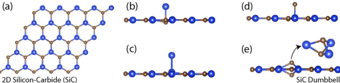
Figure 2: Equilibrium binding structures of C and Si adatoms on graphene like structure of SiC. (a) Top view of compound SiC displaying a planar honeycomb structure. (b) Si adatom on C host atom; (c) Si adatom on Si host atom; (d) C adatom on Si host atom are adsorbed at the head-on positions rather than forming a dumbbell structure. (e) C adatom on host C atom of SiC forming a DB structure. Si and C atoms are indicated by large blue and small brown balls, respectively.
Table 1: Adsorption of Group IV adatoms on single layer honeycomb structures of Group IV elements, namely graphene, silicene, and germanene in a 5×5 supercell: Substrate (graphene, silicene or germanene); adatom; types of binding structure (B=bridge; S=substitution; DB=dumbbell); nearest adatom-substrate atom distance d (values in parenthesis are D1-D2 distance in DB structures.); the lattice constant of the hexagonal unit cell of adatoms,a;
magnetic moment per supercell (µ); electronic state(numeral indicates the minimum band gap in eV, HSE band gaps are given in parenthesis); binding energy,Eb.
Substrate Adatom Structure d(Å) a(Å) µ (µB) Elec. State (eV) Eb(eV)
Graphene C B 1.52 12.35 0.4 metal 1.670 Graphene Si B 2.21 12.39 1.6 metal 0.799 Graphene Ge B 2.41 12.41 1.6 metal 0.711 Graphene Sn B 2.69 12.36 1.6 metal 0.808 Silicene C S 1.96 19.24 2.0 0.26 (0.66) 5.890 Silicene Si DB 2.40 (2.70) 19.28 2.0 0.08 (0.50) 4.017 Silicene Ge DB 2.51 (2.80) 19.31 2.0 0.06 (0.47) 3.612 Silicene Sn DB 2.73 (2.97) 19.21 2.0 0.09 (0.38) 3.200 Germanene C S 2.02 20.07 2.0 0.10 (0.42) 5.026 Germanene Si DB 2.46 (2.83) 19.87 2.0 0.06 (0.39) 3.200 Germanene Ge DB 2.57 (2.93) 19.89 2.0 0.06 (0.35) 3.397 Germanene Sn DB 2.76 (3.09) 20.01 2.0 0.08 (0.30) 3.080
stability, adsorption of Si, Ge and Sn adatoms on stanene do not form DB structures, rather they un-dergo local structural instability, followed by lo-cal destruction of single layer honeycomb struc-ture upon adsorption of Si, Ge and Sn adatoms. Instability occurred not only in the course struc-ture optimization of adatom+stanene system us-ing structure optimization usus-ing conjugate gradi-ent method, but also in ab-initio MD calculations at low temperature.
DB structures form without any energy barrier once Si, Ge and Sn adatoms are placed on sil-icene or germanene.23 The DB structure is of par-ticular interest since specific periodic patterns of DBs on silicene or germanene can construct sta-ble derivative structures which can have higher co-hesive energy with different electronic and mag-netic properties compared to parent silicene and germanene.8,21,24,27These derivatives have shown to be crucial for the growth of multilayer sil-icene and germanene on Ag and Au substrates, re-spectively.27 In fact, stacking of these derivatives can make stable thin films7,27or 3D bulk layered structures, namely silicite and germanite, display-ing rather different electronic and optical proper-ties.21 Briefly, the synthesis of derivatives com-posed of silicene and germanene patterned by DBs of Si or Ge and their alloys pave the way towards nanostructures with physical properties different from their parent cubic diamond structure, cdSi or cdGe. Our results obtained from structure opti-mization indicate that the binding energy of a sin-gle DB on silicene and germanene is rather high and ranges between 4.01 eV and 3.08 eV. Gener-ally, while the binding energies decrease, D1-D2
distances increase as the row number of the Group IV adatom increases. We note that DB patterned phases of silicene and germanene display a side view of atoms; in particular D1and D2nematic
or-bitals are reminiscent of X-X bonds of transition metal dichalcogenides, MX2.26 However, the FDS
structure consisting of silicene having three DBs at the alternating corners of hexagon, which is, in fact, very similar to single layer MX2, was found
to be unstable.27
It is known that single layer Group IV-IV com-pounds, like SiC and SiGe6can be constructed. In SiC, Si and C atoms are located at the alternating corners of the hexagon to make a planar, graphene
like structure with a 2.5 eV indirect band gap. Here, the binding structures of C and Si adatoms on C and Si host atoms of SiC are of interest. In spite of the fact that C adatom is adsorbed at B-site on graphene and substitutes Si host atom on sil-icene, C adatom forms a DB structure on SiC when placed on top of the host C atom. While the DB structure made of two C atoms is the second most energetic binding structure of graphene,42 DB of C atoms becomes the most energetic binding struc-ture in SiC. On the other hand, C adatom on top of host Si, Si adatom on top of host C and Si adatom on top of host Si atom of SiC are bound at the top site (T). Even if the adatoms were displaced from the top site or were placed to B-site, they always moved to the equilibrium T site to minimize the total energy. In 2, these four equilibrium bind-ing structures, each with a magnetic moment of 2.0 µB/per cell, are illustrated.
The SiGe honeycomb structure, where Si and Ge atoms are alternatingly located at the corner of hexagon, is another important compound we con-sidered in this study. The buckling between adja-cent Si and Ge is larger than that in silicene, but smaller than that in germanene. It is stable and has π -π∗bands crossing linearly at the Fermi level, if small spin-orbit coupling is neglected. Four types of DBs, namely Si-Si, Ge-Si, Si-Ge and Ge-Ge DBs can be constructed, each having a magnetic ground state of 2.0 µb/per cell; but attributing
dif-ferent physical properties to the SiGe substrate. The crucial issue to address now is whether the adatom adsorbed substrates are stable. While optimized structure through conjugate gradient method provides evidence that the structure in hand is stable at T=0 K, this may correspond to a shallow minimum and hence the system may be destabilized at elevated temperatures. In fact, we found that the adsorption of all Group IV adatoms caused stanene to undergo a structural instabil-ity. Here we explored the stability of Group IV adatoms adsorbed on silicene and germanene at elevated temperature by performing ab-initio MD calculations at finite temperatures, whose details are explained in the Methods section. Even at a temperature as high as T = 1500K, the systems presented in 1 remained stable. We also note that similar MD calculations were carried out to test whether bare stanene by itself is stable at elevated
temperatures. While free standing stanene main-tained its structural stability for one picosecond at 400K, its structure is massively deformed during MD simulation at 600K. This explains why the structure of stanene is destroyed upon the adsorp-tion of Group IV atoms treated in this study. It should be noted that stanene grown on substrate can attain stability and remain stable upon the ad-sorption of adatoms.
Electronic Structures
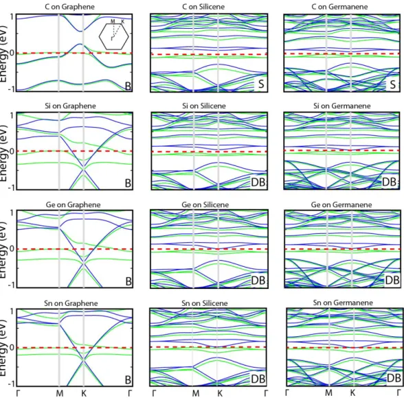
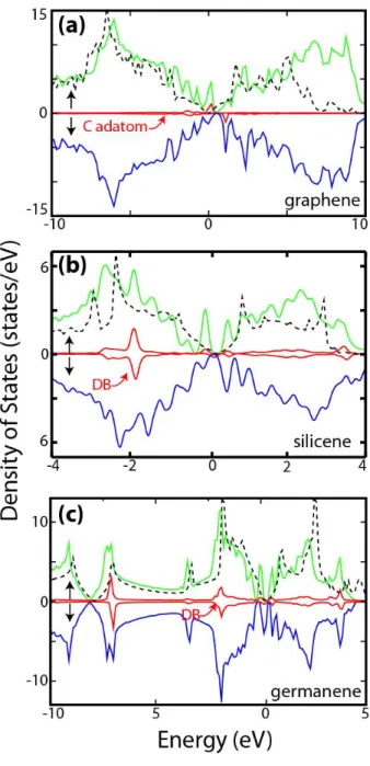
Group IV adatoms give rise to important changes also in the magnetic and electronic properties. In 3 we presented the total density of states for C, Si and Ge adatoms adsorbed on graphene, silicene and germanene, respectively. The partial density of states of adatoms depicts the contribution of the adatom in the relevant energy range. For the sake of comparison, the density of states of cor-responding bare substrate is also shown in each panel. While bare graphene, silicene and ger-manene all have nonmagnetic ground state, they attain magnetic ground state upon the adsorption of adatoms. The dominant effect of the adatom appears as sharp peaks near the band edges, which originate from the flat bands constructed from the mixing of orbitals of adatoms and host atoms at close proximity. In 4 we present the electronic band structures of the optimized structures for C, Si, Ge and Sn adatoms adsorbed also on graphene, silicene and germanene. In addition, we improve the band structures with HSE as shown in 5. Sim-ilar to binding structure and energetics of adatom, the effect of the adatom on the electronic and magnetic structures are explored using a super-cell model. If the spin-orbit coupling is neglected, bare graphene, silicene, as well as germanene are semimetals with conduction and valence bands crossing linearly at the Fermi level (EF) carrying
massless Dirac Fermion behavior.2 The localized (or resonance) states of single, isolated Group IV adatoms can occur below or above their EF.
How-ever, within the periodically repeating 5×5 super-cell model with minute DB-DB coupling, these states are slightly broadened and form adatom bands. Therefore, the flat bands in 4 are associ-ated with the localized states due to adatoms. The
effect of the adatoms on the electronic and mag-netic properties are summarized also in 1. On sil-icene and germanene they lead similar electronic and magnetic states. DB formations on silicene and germanene in 5×5 supercell periodicity re-sult in ferromagnetic semiconductors with small band gaps of 0.06 - 0.12 eV within DFT-GGA. The magnetic moment per supercell is calculated to be 2.0 µB. The energy difference between magnetic
and non-magnetic state is rather small (∼0.1 eV) for all cases indicating that it is a low temperature property. In what follows we present a compre-hensive analysis of electronic band structures.
In 4, flat bands at the EF are associated with the
states localized at carbon adatom at B-site forming bridge bonds with two nearest neighbor C atoms of graphene. These bands, which pin the EF are
de-rived from py and pz orbitals of carbon adatom at
B-site. In the 5×5 supercell, the crossing bands of bare graphene split and EF dips into the
va-lence band to attribute metallic character. The net magnetic moment of each supercell is µ =1.6µB.
Si, Ge and Sn adatoms, which are also bonded to graphene at B-site give rise to metallic band struc-tures as shown in 4. The π∗− π bands of bare graphene, which cross linearly at the K-point of Brillouin zone dip 0.1-0.3 eV below the EF upon
the adsorption of Si, Ge and Sn adatoms at B-site. It appears that the flat bands associated with the lo-calized p-orbital states of Si, Ge and Sn adsorbate occur above the band crossing point and pin the EF. In addition, each supercell attains a magnetic
moment of 2 µB. This is a significant effect, which
makes non-magnetic graphene, silicene, and ger-manene spin-polarized.
The flat bands shown in 4 near the band gap of the substitutional C adatom forming 5×5 pat-tern in silicene and germanene are associated with the localized (or resonance) p-orbital states of the adatom as well as the p-orbital states of the host Si atom that is displaced from its regular position as indicated by the small arrow in 1(b). The effect of substitutional C atom is the splitting of the π∗− π bands crossing at the k-point and hence trans-forming the semi-metal bare silicene/germanene to semiconductor. The lower valence bands are also affected from the substitutional C atom.
Upon the formation of Si-DB on silicene the spin-degeneracy of the bands are lifted as shown
Figure 4: Electronic band structures of monolayer graphene, germanene, and silicene with adatoms C, Si, Ge and Sn, which form a 5×5 supercell or pattern. In the spin polarized systems, spin up and spin down bands are shown with green and blue lines. The zero of energy shown by red dashed line is set to the energy of highest occupied state. Binding structures (as B, S, DB) are indicated in each panel. Brillouin zone and symmetry directions are shown by inset.
Figure 3: Total density of states for (a) C on graphene (b) Si on silicene and (c) Ge on germanene. The par-tial DOS of the adatoms are indicated by red lines and multiplied by a factor of2for better visualization. Spin up and spin down states are shown with green and blue lines, respectively. DOS of pure graphene, silicene and germanene are also indicated by the dashed curves in the plots.
Figure 5: Electronic band structures are calculated by using HSE for single layer silicene and germanene with adatoms C, Si, Ge and Sn, which form a 5×5 supercell or pattern. In the spin polarized systems, spin up and spin down bands are shown with green and blue lines. The zero of energy shown by red dashed line is set to the energy of highest occupied state. Binding structures (as B, S, DB) are indicated in each panel.
in 4 and narrow band gap opens between spin up and spin down bands. It should be noted that the electronic and magnetic properties of silicene pat-terned by Si-DB strongly depend on the size and symmetry of the DB pattern. Similar effects occur also with Ge-DB and Sn-DB forming 5×5 pattern in silicene and germanene, except that the band gap between spin up and spin down bands is closed as the row number of adatom increases.
Considering the fact that the energy band gaps are underestimated by standard DFT methods, we repeat the calculations by using hybrid function-als,34except for graphene where all configurations are metallic. According to those results all the sys-tems are ferromagnetic semiconductor confirming what is obtained at DFT-GGA level with an ex-pected increase in energy band gaps. The cor-rected band gaps are given in parenthesis in 1. In-terestingly, energy band gaps decrease as the row number of the adatom as well as the substrate in-creases.
The optical properties of the two 2D honey-comb Group-IV crystals; silicene and germanene have been briefly investigated by calculating the frequency dependent complex dielectric function εi(ω) for normal incidence. The optical
absorp-tion is determined by the imaginary part of the di-electric function. The main peaks of absorption of both structures are related with the inter-band transitions that come into play. This finding is also supported in the works which study the infrared absorption spectra of silicene and germanene.43,44 In fact, both materials are known to be attractive candidates for nano-optoelectronic applications, since they display electronic and optical bandgaps which are within or in the vicinity of the visi-ble part of the electromagnetic spectrum. Here the effects of Si and Ge adatoms are investigated by comparing the calculated optical properties be-fore and after dumbbell formation. Two differ-ent coverages of dumbbells leading to (√3 ×√3) dumbbell structure and hexagonal dumbbell struc-ture (HDS) were investigated.8,27 The imaginary dielectric function is displayed in 6 for both sys-tems. Accordingly, bare silicene shows optical ac-tivity around 1 eV in the relatively early frequency regime, which extends to beyond 3 eV towards higher photon energies. As for the (√3 ×√3) and HDS supercells of silicene, intense peaks of
absorption are observed around 0.6 and 0.8 eV, respectively. Moreover, the second major peaks for both are concentrated in the range of 2.8-4.4 eV. ε2(ω) of bare germanene, on the other hand,
displays more similar features to its doped coun-terparts, when compared to silicene. An early strong absorption phenomenon takes place below 0.3 eV for both bare and (√3 ×√3) forms of germanene. On the contrary, Ge-HDS shows a first peak around 1.1 eV. Some important prelim-inary results can be summarized as: (i) The in-tensities of the absorption peaks vary (i.e. be-come more distinguished) depending on the struc-ture, when doped. (ii) The optically active region can be tuned by doping. Apparently, the periodic structure of DBs may introduce crucial effects on the optical absorption spectra, which may lead to certain potential applications in the visible range. Further investigation of the optical properties of DB-structures of silicene and germanene is con-sidered as the topic of a future publication, which are aimed to be studied also at the level of many-body GW corrections in order to introduce further accuracy to the peaks of absorption.
Migration of Dumbbells on
Sil-icene and Germanene
As mentioned above, as soon as specific adatoms land on specific substrates, DBs can form through an exothermic process without an energy bar-rier. Moreover, DB-DB coupling is attractive un-til the first nearest neighbor separation.8,24 Conse-quently, as Si, Ge and Sn adatoms continue to land on silicene or germanene, firstly the domains of DBs form, eventually they join to cover the surface uniformly. In this respect, the migration or diffu-sion of DBs on silicene and germanene is crucial for the formation of various phases derived from silicene and germanene through their coverage by DBs in different concentration and symmetry. The energetics of the migration and the minimum en-ergy barrier of single Si-DB on silicene and Ge-DB on germanene are investigated between the first and second nearest neighbors as shown in 7 using nudged elastic band (NEB) method.45 The difference of the maximum and minimum total energy along the path corresponds to the energy
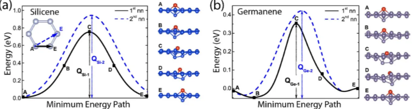
Figure 7: (a) Migration of Si-DB on silicene and (b) Ge-DB on germanene. Energetics and the migration energy barrier (Q) of a single, isolated DB between the first and second nearest neighbors are shown by the inset in the left panel. The barriers are calculated using the nudged elastic band (NEB) method. Snapshots of the atomic configurations taken at stages A, B, C, D and E during the migration of DB to the first nearest neighbor site are also presented to illustrate the mechanism of diffusion.
Figure 6: The optical absorption spectra of bare (black curve), (√3 ×√3) (green curve with dots) and HDS (dashed blue curve) structures of silicene (top) and ger-manene (bottom), respectively. Structures are shown in the inset plots.
barrier, Q. The energy barrier to the migration of D1 of Si-DB along the straight path between
the two first nearest neighbor atoms of silicene is Q=0.75 eV (minima are denoted by A and max-ima by C in 7). Similar to the binding energies in 1, the diffusion barrier of Ge-DB on germanene is lower than that of Si-DB on silicene. The bar-rier along the path between the second nearest neighbor is slightly higher. In a concerted ac-tion, as D1 moves along the path, D2 raises and
eventually attains its original position at the cor-ner of the buckled hexagon. On the contrary, the host atom at the first nearest neighbor site moves down as D1 approaches and eventually the
migra-tion is completed with the construcmigra-tion of a new DB at the first nearest neighbor site. Snap-shots of atomic structure in the course of migration is also in shown 7. Low energy barrier to migration assures high mobility of DBs on silicene and ger-manene substrates needed for multilayer growth. The local minima denoted by B (which is ener-getically lower than A) for Ge-DB on germanene is considered to be due to a local unstable defor-mation appearing at that instantaneous atomic ar-rangement.
Conclusions
In this paper we investigated the binding of Group IV adatoms (C, Si, Ge and Sn) to single-layer, honeycomb structures of these atoms, namely graphene, silicene and germanene. The adsorp-tion to stanene is not included since this
struc-ture is prone to instability upon the adsorption of any of the Group IV adatoms. Depending on the row number of a Group IV adatom, as well as substrates, we deduced three types of equilib-rium binding structures. Isolated adatoms, as well as those forming periodically repeating supercells on graphene, silicene and germanene give rise to changes in electronic, magnetic and optical prop-erties. Among the three types of binding struc-tures, the dumbbell structure is of particular im-portance, since stable new phases of silicene and germanene can be derived from their periodic cov-erage with DBs. Dumbbell structures are also con-structed on single layer, Group IV-IV compounds. The calculated energy barrier to the migration or diffusion of DBs on substrates is found to be low. This implies that DBs are rather mobile and cover the substrates as long as there is sufficient amount of incoming adatoms. By stacking these single layer phases one can grow thin film alloys and lay-ered bulk structure of silicene and germanene.
Acknowledgement
The computational resources is provided by TUBITAK ULAKBIM, High Performance and Grid Computing Center (TR-Grid e-Infrastructure). VOÖ and SC acknowledge fi-nancial support from the Academy of Sciences of Turkey(TUBA). ED acknowledges support from Bilim Akademisi - The Science Academy, Turkey under the BAGEP program. This work is partially supported by TUBITAK under the Project No. 113T050.
References
(1) Durgun, E.; Tongay, S.; Ciraci, S. Silicon and III-V Compound Nanotubes: Structural and Electronic Properties. Phys. Rev. B 2005, 72, 075420.
(2) Cahangirov, S.; Topsakal, M.; Aktürk, E.; ¸Sahin, H.; Ciraci, S. Two- and One-Dimensional Honeycomb Structures of Sili-con and Germanium. Phys. Rev. Lett. 2009, 102, 236804.
(3) De Padova, P.; Quaresima, C.; Ottaviani, C.;
Sheverdyaeva, P. M.; Moras, P.; Carbone, C.; Topwal, D.; Olivieri, B.; Kara, A.; Oughad-dou, H.; Aufray, B.; Le Lay, G. Evidence of Graphene-like Electronic Signature in Sil-icene Nanoribbons. Appl. Phys. Lett. 2010, 96, 261905.
(4) Vogt, P.; De Padova, P.; Quaresima, C.; Avila, J.; Frantzeskakis, E.; Asensio, M. C.; Resta, A.; Ealet, B.; Le Lay, G. Sil-icene: Compelling Experimental Evidence for Graphenelike Two-Dimensional Silicon. Phys. Rev. Lett.2012, 108, 155501.
(5) Van Hoang, V.; Mi, H. T. C. Free-standing Silicene Obtained by Cooling from 2D Liq-uid Si: Structure and Thermodynamic Prop-erties. J. Phys. D: Appl. Phys. 2014, 47, 495303.
(6) ¸Sahin, H.; Cahangirov, S.; Topsakal, M.; Bekaroglu, E.; Akturk, E.; Senger, R. T.; Ciraci, S. Monolayer Honeycomb Structures of Group-IV Elements and III-V Binary Compounds: First-Principles Calculations. Phys. Rev. B2009, 80, 155453.
(7) De Padova, P.; Vogt, P.; Resta, A.; Avila, J.; Razado-Colambo, I.; Quaresima, C.; Otta-viani, C.; Olivieri, B.; Bruhn, T.; Hira-hara, T.; Shirai, T.; Hasegawa, S.; Car-men Asensio, M.; Le Lay, G. Evidence of Dirac Fermions in Multilayer Silicene. Appl. Phys. Lett.2013, 102, 163106.
(8) Özçelik, V. O.; Durgun, E.; Ciraci, S. New Phases of Germanene. J. Phys. Chem. Lett. 2014, 5, 2694–2699.
(9) Rachel, S.; Ezawa, M. Giant Magnetoresis-tance and Perfect Spin Filter in Silicene, Ger-manene, and Stanene. Phys. Rev. B 2014, 89, 195303.
(10) Özçelik, V. O.; Cahangirov, S.; Ciraci, S. Sta-ble Single-Layer Honeycomblike Structure of Silica. Phys. Rev. Lett. 2014, 112, 246803. (11) Xu, Y.; Yan, B.; Zhang, H.-J.; Wang, J.; Xu, G.; Tang, P.; Duan, W.; Zhang, S.-C. Large-Gap Quantum Spin Hall Insulators
in Tin Films. Phys. Rev. Lett. 2013, 111, 136804.
(12) Liu, C.-C.; Jiang, H.; Yao, Y. Low-energy Effective Hamiltonian Involving Spin-orbit Coupling in Silicene and Two-dimensional Germanium and Tin. Phys. Rev. B 2011, 84, 195430.
(13) Tang, P.; Chen, P.; Cao, W.; Huang, H.; Ca-hangirov, S.; Xian, L.; Xu, Y.; Zhang, S.-C.; Duan, W.; Rubio, A. Stable Two-dimensional Dumbbell Stanene: A Quantum Spin Hall In-sulator. Phys. Rev. B 2014, 90, 121408. (14) Van den Broek, B.; Houssa, M.; Scalise, E.;
Pourtois, G.; Afanasev, V. V.; Stesmans, A. Two-dimensional Hexagonal Tin: Ab Ini-tio Geometry, Stability, Electronic Structure and Functionalization. 2D Mater. 2014, 1, 021004.
(15) Ataca, C.; Sahin, H.; Ciraci, S. Stable, Single-layer MX2 Transition Metal Oxides
and Dichalcogenides in a Honeycomb-like Structure. J. Phys. Chem. C 2012, 116, 8983–8999.
(16) Tongay, S.; Zhou, J.; Ataca, C.; Lo, K.; Matthews, T. S.; Li, J.; Grossman, J. C.; Wu, J. Thermally Driven Crossover from In-direct toward Direct Bandgap in 2D Semi-conductors: MoSe2 versus MoS2. Nano Lett.
2012, 12, 5576–5580.
(17) Novoselov, K. S.; Jiang, D.; Schedin, F.; Booth, T. J.; Khotkevich, V. V.; Moro-zov, S. V.; Geim, A. K. Two-dimensional Atomic Crystals. P. Natl. Acad. Sci. USA 2005, 102, 10451–10453.
(18) Wang, Z.; Zhao, K.; Li, H.; Liu, Z.; Shi, Z.; Lu, J.; Suenaga, K.; Joung, S.-K.; Okazaki, T.; Jin, Z.; Gu, Z.; Gao, Z.; Ii-jama, S. Ultra-narrow W S2Nanoribbons
En-capsulated in Carbon Nanotubes. J. Mater. Chem.2011, 21, 171–180.
(19) Vogt, P.; Capiod, P.; Berthe, M.; Resta, A.; De Padova, P.; Bruhn, T.; Le Lay, G.; Gran-didier, B. Synthesis and Electrical
Conduc-tivity of Multilayer Silicene. Appl. Phys. Lett. 2014, 104, 021602.
(20) Padova, P. D.; Ottaviani, C.; Quaresima, C.; Olivieri, B.; Imperatori, P.; Salomon, E.; Angot, T.; Quagliano, L.; Romano, C.; Vona, A.; Muniz-Miranda, M.; Generosi, A.; Paci, B.; Lay, G. L. 24h Stability of Thick Multilayer Silicene in Air. 2D Mater. 2014, 1, 021003.
(21) Cahangirov, S.; Özçelik, V. O.; Rubio, A.; Ciraci, S. Silicite: The Layered Allotrope of Silicon. Phys. Rev. B 2014, 90, 085426. (22) Tritsaris, G. A.; Kaxiras, E.; Meng, S.;
Wang, E. Adsorption and Diffusion of Lithium on Layered Silicon for Li-ion Stor-age. Nano Lett. 2013, 13, 2258–2263. (23) Özçelik, V. O.; Gurel, H. H.; Ciraci, S.
Self-healing of Vacancy Defects in Single-layer Graphene and Silicene. Phys. Rev. B 2013, 88, 045440.
(24) Özçelik, V. O.; Ciraci, S. Local Reconstruc-tions of Silicene Induced by Adatoms. J. Phys. Chem. C2013, 117, 26305–26315. (25) Kaltsas, D.; Tsetseris, L. Stability and
Elec-tronic Properties of Ultrathin Films of Sil-icon and Germanium. Phys. Chem. Chem. Phys.2013, 15, 9710–9715.
(26) Gimbert, F.; Lee, C.-C.; Friedlein, R.; Fleurence, A.; Yamada-Takamura, Y.; Ozaki, T. Diverse Forms of Bonding in Two-dimensional Si Allotropes: Nematic Orbitals in the MoS2Structure. Phys. Rev. B
2014, 90, 165423.
(27) Cahangirov, S.; Özçelik, V. O.; Xian, L.; Avila, J.; Cho, S.; Asensio, M. C.; Ciraci, S.; Rubio, A. Atomic Structure of the√3 ×√3 Phase of Silicene on Ag(111). Phys. Rev. B 2014, 90, 035448.
(28) Kohn, W.; Sham, L. J. Self-Consistent Equa-tions Including Exchange and Correlation Effects. Phys. Rev. 1965, 140, A1133– A1138.
(29) Hohenberg, P.; Kohn, W. Inhomogeneous Electron Gas. Phys. Rev. 1964, 136, B864– B871.
(30) Grimme, S. Semiempirical GGA-type Den-sity Functional Constructed with a Long-Range Dispersion Correction. J. Comput. Chem.2006, 27, 1787–1799.
(31) Blöchl, P. E. Projector Augmented-wave Method. Phys. Rev. B 1994, 50, 17953– 17979.
(32) Perdew, J. P.; Burke, K.; Ernzerhof, M. Gen-eralized Gradient Approximation Made Sim-ple. Phys. Rev. Lett. 1996, 77, 3865–3868. (33) Kresse, G.; Furthmüller, J. Efficient Iterative
Schemes for Ab-initio Total-energy Calcu-lations Using a Plane-wave Basis set. Phys. Rev. B1996, 54, 11169–11186.
(34) Paier, J.; Marsman, M.; Hummer, K.; Kresse, G.; Gerber, I. C.; Ángyán, J. G. Screened Hybrid Density Functionals Ap-plied to Solids. J. Chem. Phys. 2006, 124, 154709.
(35) Heyd, J.; Scuseria, G. E.; Ernzerhof, M. Hybrid functionals based on a screened Coulomb potential. J. Chem. Phys. 2003, 118, 8207–8215.
(36) Gajdoš, M.; Hummer, K.; Kresse, G.; Furthmüller, J.; Bechstedt, F. Linear Op-tical Properties in the Projector-augmented Wave Methodology. Phys. Rev. B 2006, 73, 045112.
(37) Tongay, S.; Senger, R. T.; Dag, S.; Ciraci, S. Ab-initio Electron Transport Calculations of Carbon Based String Structures. Phys. Rev. Lett.2004, 93, 136404.
(38) Fan, X. F.; Liu, L.; Lin, J. Y.; Shen, Z. X.; Kuo, J.-L. Density Functional Theory Study of Finite Carbon Chains. ACS Nano 2009, 3, 3788–3794.
(39) Özçelik, V. O.; Ciraci, S. Self-assembly Mechanisms of Short Atomic Chains on Single-layer Graphene and Boron Nitride. Phys. Rev. B2012, 86, 155421.
(40) Ataca, C.; Ciraci, S. Perpendicular Growth of Carbon Chains on Graphene from First-principles. Phys. Rev. B 2011, 83, 235417. (41) Ataca, C.; Aktürk, E.; ¸Sahin, H.; Ciraci, S.
Adsorption of Carbon Adatoms to Graphene and Its Nanoribbons. J. Appl. Phys. 2011, 109, 013704.
(42) Aktürk, E.; Ataca, C.; Ciraci, S. Ef-fects of Silicon and Germanium Adsorbed on Graphene. Appl. Phys. Lett. 2010, 96, 123112.
(43) Matthes, L.; Gori, P.; Pulci, O.; Bechstedt, F. Universal Infrared Absorbance of Two-Dimensional Honeycomb Group-IV Crys-tals. Phys. Rev. B 2013, 87, 035438.
(44) Matthes, L.; Pulci, O.; Bechstedt, F. Mas-sive Dirac Quasiparticles in the Optical Ab-sorbance of Graphene, Silicene, Germanene, and Tinene. J. Phys.: Condens. Matter 2013, 25, 395305.
(45) Henkelman, G.; Uberuaga, B. P.; Jónsson, H. A Climbing Image Nudged Elastic Band Method for Finding Saddle Points and Min-imum Energy Paths. J. Chem. Phys. 2000, 113, 9901–9904.