DESIGN
AND
IMPLEMENTATION
OF
A
GENERAL
PURPOSE MEDIAN
FILTER
UNIT
IN
VLSI
A THESIS
SUBMITTED TO THE DEPARTMENT OF ELECTRICAL AND
ELECTRONICS ENGINEERING
AND THE INSTITUTE OF ENGINEERING AND SCIENCES
OF BILKENT UNIVERSITY
IN PARTIAL FULFILLMENT OF THE REQUIREMENTS
for the
D
egree ofMASTER OF SCIENCE
By
Mustafa Karaman
October 1988
I certify that I have read this thesis and that in my
opinion it is fully adequate, in scope and in quality, as
a thesis for the degree of Master of Science.
Asst. Prof. Dr. Levent Onural(PrincipalAdvisor)
I certify that I have read this thesis and that in my
opinion it is fully adequate, in scope and in quality, as a thesis for the degree of Master of Science.
__________________
Assoc. Prof. Dr. AbdullahAtalar (Second supervisor)
I certify that I have read this thesis and that in my opinion it is fully adequate, in scope and in quality, as a thesis for the degree of Masterof Science.
Asst. Prof. Dr. Mehmet Ali Tan
Approvedfor the Instituteof Engineering and Sciences:
© Copyright 1988
by
ABSTRACT
DESIGN AND IMPLEMENTATION OF
A GENERAL PURPOSE MEDIAN FILTER UNIT
IN VLSI
Mustafa Karaman
M.S. in Electrical and Electronics Engineering
Supervisors: Asst. Prof. Dr. Levent Onural
and Assoc. Prof. Dr. Abdullah Atalar
October 1988
The median of a group, containing anodd number of elements, is defined as
the middle element, when the elements of the group are sorted. A median
filter finds the median of a number of elements at its inputs. Medianfilters
are frequently used in many signal, and image processing applications for smoothingof the noisy signals and images while at the sametime preserving
the edge information.
The required window size, speed, and the word length of the median
filters vary depending on the applications. In order to meet these changing demands a general purpose median filter unit configuration isproposed. The
unit consists of two single-chip median filters. One of the chips is designed for unlimited word-length and extensibility to larger window sizes whereas the other one is for real-time video applications. The networks of the chips
are basedon the odd/even transposition sorting. The chips are implemented
in3-^mM2CMOS by using full-custom VLSIdesign techniques. For physical
testing of the chips, the test vectors and the corresponding outputs of the chips are generated by using software tools written forthis purpose.
In this thesis, the algorithms, VLSI implementations, simulation results,
testing, and applications of the chips are presented.
Keywords: Median filters,signaland image processing,signal processing hardware, VLSI implementation, VLSI testing.
ÖZET
GENEL AMAÇLI BİR ORTANCA SÜZGECİ BİRİMİNİN
VLSI TASARIMI VE GERÇEKLEŞTİRİLMESİ
Mustafa Karaman
Elektrik ve Elektronik Mühendisliği Yüksek Lisans
Tez Yöneticileri: Yrd. Doç. Dr. Levent Onural
ve Doç. Dr. Abdullah Atalar
Ekim 1988
Tek sayıdaki verilerin oluşturduğubir kümenin ortancası (medyanı), verilerin büyüklüklerine göre sıralanması ile elde edilen dizinin tam ortasındaki veri
olarak tanımlanır. Bir ortanca süzgeci, girişindeki verilerin ortancasını bu lur. Ortanca süzgeçleri, bir çok işaret ve görüntü işleme uygulamalarında
kullanılmaktadır. Kenar keskinliğinin korunması ve impulsive gürültülerin
iyi ayıklanması bu süzgeçlerinen önemli özelliklerindendir.
Ortanca süzgeçlerinin gereken pencere büyüklüğü, hızı ve bit uzunluğu uygulamaya bağlı olarak değişmektedir. Bu değişen gereksinimleri karşılayabil mek için genel amaçlıbirortancasüzgecibirimi önerilmiştir. Bu birim,iki tek yonga ortancasüzgecinden oluşmaktadır. Yongalardan biri, sınırsız bit uzun
luğu ve daha büyük pencerelere genişletilebilecek şekilde diğeri ise on-line
uygulamalarında kullanılabilecek hızlara erişebilecek şekilde tasarlanmıştır. Yongalarda kullanılan ağlar tek/çift değiştirimle sıralamayöntemine dayalıdır.
Yongalar, full-customVLSI tasarım tekniklerikullanılarak 3-/ım M2CMOS’da gerçekleştirilmiştir. Yongaların üretiminden sonra yapılacak testlerinde kul
lanılacak olan giriş işaretleri ve bunlara ait çıkış işaretleri bu amaçlar için
yazılmışbilgisayar programlan yardımıyla elde edilmiştir.
Bu tezde, söz konusu yongaların algoritmaları, VLSI gerçekleştirimleri, simülasyon sonuçlan, testleri ve uygulamalansunulmaktadır.
Anahtar Kelimeler: Ortanca süzgeçleri, işaret ve görüntü işleme, işaret
işleme donamım, VLSI gerçekleştirin!, VLSI test.
ACKNOWLEDGEMENT
I would like to express my deep thanks to my thesis supervisors Asst.
Prof. Dr. Levent Onural and Assoc. Prof. Dr. Abdullah Atalar for their
supervisions, guidances, and encouragements during this research.
I am grateful to my friend I. Enis Ungan for his efforts to modify the VLSI tools and to developnew tools, andto my friend Satılmış Topçufor his valuableideas on VLSI testing of the chips.
TABLE OF CONTENTS
1 INTRODUCTION 1
1.1 Median Filter... 1
1.2 Motivation and Approach... 2
1.3 On the Performance ofAlgorithms... 3
1.4 Benefits... 4
1.5 Organization ofThesis... 4
2 A SURVEY OF MEDIAN FILTERING 5 2.1 Median Filtering Techniques... 5
2.1.1 Finding Root Signal... 5
2.1.2 Recursive Median Filtering... 6
2.1.3 Generalized Median Filtering... 6
2.1.4 Separable Median Filtering... 6
2.1.5 Weighted Median Filtering... 7
2.2 Median Filtering Algorithms ... 7
3 GENERAL PURPOSE MEDIAN FILTER 10 3.1 Odd/Even Transposition Sorting Network... 10
3.2 Extensible Median Filter Network ... ... . 12
3.3 Real-Time Median Filter Network ... 16
3.4 Feasibility ofVLSIImplementation... 18
4 VLSI DESIGN METHODOLOGY 21 4.1 VLSI Design Approach... 21
4.2 CircuitTechnique... 25
5 VLSI IMPLEMENTATION 29
5.1 Implementation of the Extensible Median Filter ... 29
5.1.1 Compare-and-Swap Unit-1 (CSU1)... 31
5.1.2 Delay Unit... 34
5.1.3 Clock Buffers... 34
5.1.4 Chip Overall Layout... 38
5.1.5 An Overview of the Extensible Median Filter Chip . . 38
5.1.6 Testing of the Extensible MedianFilter Chip... 44
5.2 Implementation of the Real-Time Median Filter... 46
5.2.1 Compare-and-Swap Unit-2 (CSU2)... 46
5.2.2 Delay Unit... 51
5.2.3 Clock Buffers... 51
5.2.4 Chip Overall Layout... 51
5.2.5 An Overview of the Real-Time Median Filter Chip . . 55 5.2.6 Testingof the Real-Time Median Filter Chip... 55
5.3 Applications of the Chips... 59
6 RESULTS AND CONCLUSIONS 62
APPENDIX 70
LIST OF FIGURES
3.1 The ordinary odd/eventransposition network (w = 9)... 11
3.2 The extensible median filter network (w = 9)... 13
3.3 The compare-and-swap unit-1 (CSU1): a) block diagram, b) state diagram, c) operations... 14
3.4 Interconnections of the extensible median filter networks for w = 9... 15
3.5 The real-time median filter network... 17
3.6 The compare-and-swap unit-2 (CSU2)... 18
4.1 The VLSI design steps... 23
5.1 The floorplan... 30
5.2 The power and clock distribution scheme... 30
5.3 Circuit diagramof the CSU1... 32
5.4 Layout of the CSU1... 32
5.5 Timing simulation results of the CSU1... 33
5.6 Circuit diagramof the shift register cell... 35
5.7 Layout of the shift register cell... 35
5.8 Timing simulation results of the shift register cell... 36
5.9 Circuit diagrams of the clock buffers... 37
5.10 Layouts of theclock buffers: a) noninverting, b) inverting. . . 37
5.11 Timing simulation results of the clock buffers: a) for 50 MHz, b) for 20 MHz... 39
5.12 Complete layout of the extensible medianfilter chip... 40
5.13 Logicsimulationresults of the extensible median filter chip. . 41
5.14 Pin configuration of the extensible median filterchip... 42
5.15 Timing diagrams for data load and read operations of the ex tensible median filter chip... 43
5.17 The floor plan... 47
5.18 The power and clock distribution scheme... 47
5.19 Circuit diagram of the CSU2... 49
5.20 Layout of the CSU2... 49
5.21 Timingsimulation results of the CSU2... 50
5.22 Circuit diagrams of the delay units used at the: a) inputs, b) internal stages of the the real-time medianfilter chip... 52
5.23 Layouts of the delay units used at the: a) inputs, b) internal stages of the the real-time median filter chip... 52
5.24 Timing simulations of the delay units used at the: a) inputs, b) internal stages of the the real-time median filter chip. ... 53
5.25 Overall layout of the real-time median filter chip... 54
5.26 Pin configuration of the the real-time median filter chip. ... 57
5.27 Timing diagrams for the dataload and read operations of the real-time medianfilter chip... . 58
LIST OF TABLES
5.1 Logic simulation results of the CSU1... 34 5.2 Pin labels of the extensible median filter chip... 40 5.3 Functions of the I/O’s in the normal mode of the extensible
median filter chip... 43 5.4 Logic simulation results of the CSU2... 48 5.5 Logic simulation results of the real-time median filter chip. . 56
5.6 Pin labels of the the real-time median filter chip... 57
5.7 A sample of the test vectors and corresponding outputs. The
IKJ/OKJ:J’/7i input/output of the K’iA block of the real-time
median filter sorting network... 60
1. INTRODUCTION
1.1
Median
Filter
The median of a group, containing an odd number of elements, is defined
as the middle most element, when the elements of the group are sorted.
For example, given five elements, 9, 0, 23, 145, 67, to find the median, the numbers are sorted as 0, 9, 23, 67, 145 . Then, the median is 23 which is the middle most element of the sorted sequence. A median filter finds the
median of a number of elements at its input.
Inmany signal and imageprocessing applications,it is necessary to smooth
thenoisy signals whileat the sametimepreserving the edgeinformation. The
most commonly used smoothing techniques are the linear filtering [1], the av
eraging filtering [2], andthe median filtering [3,4]. The linear filters smooth
the noisy signals but also the sharp edges. In addition, the impulsive noise components can not be suppressed sufficiently by thelinear filtering and the digital implementation of the linear filters can be bulky and slow. On the other hand, the generalized mean filters have the disadvantages of allowing a small number of outlier points that distort the filtered output signal, and
also deleting the edge information. The median filters have been better al ternatives becauseof their some very interesting properties: they
• can smooth the transient changes in signal intensity (e.g., noise),
• are veryeffective for removing the impulsive noises from the signals,
• preserve the edgeinformation in the filtered signal, and
• can be implemented by using verysimple digital nonlinear operations.
Because of these properties of the median filters, they are frequently used in various signal and image processing applications, such as seismic signal
processing, speech processing, computerized tomography, medical imaging,
roboticvision, pattern recognition, peak detection, coding, and communica
tion.
In the applications forstandardmedian filteringof the signals and images, a window of size w, where w is odd, is moved along the sampled values of
signal or image, the median ((w + l)/2’nd largest one) of the samples within
the window computed and written as the output pixel corresponding to the location of thecenter of the window. Themedian computed at thisoperation
is called the running or the moving median. Since the size of the window is constant,the number of incoming elements is equalto the number ofoutgoing
elements. The detailed discussion of the theoretical analysis of the median
filtersandtheir properties can be found in [5,6,7,8,9,10,11]. The applications
of the median filters inspeech processing and imageprocessing were studied
in [12,13,14].
1.2
Motivation
and
Approach
The purpose of this study is to have anexercisein VLSIdesign by completing
a part of a project which consists of the design and implementation of a flexible VLSI image processor. Forthis purpose, the VLSI design of a general
purpose median filter unit is chosen since this unit can also be used in any signal or image processors.
Different two-dimensional applicationsrequire different window sizes and word-lengthsfor median filtering. The window size varies from 3 x 3 to quite
larger ones. Also,the required speed of the filtering operation variesdepend ing on the application. A median filter which is intended as a component of
a general purpose signal or image processor must meet these changing de
mands. For this reason, the median filter that we design should satisfy the
following constraints:
• the word-length must be unlimited,
• the filtershould be extensible to larger window sizes, and
• the filter should be able to operate at real-time rate which is about
30 mega medians persecond for a 1024 x 1024 framewith 25-30 frames per second.
We propose a solution to this problem in the form of two single-chip
median filter networks which form ageneral purpose median filter unit. The
networks are implemented in 3-micron CMOS using the full-custom VLSI design techniques. One of the chips is designed for unlimited word length
and extensibility for larger window sizes whereas the other one is for the real-time medianfiltering applications. The chips can be selectively used in a processor environment.
1.3
On
the
Performance
of
Algorithms
The algorithms that are efficient for software implementation minimize the
number of computations andhence the computationtime. InVLSI, the cost
is determined by the modularity and the internal communication between themodules. Thisis because the irregular structures and especially complex communication interconnections increase the chip area considerably. The computation is cheap inVLSI, because the recent developments offer design
ers very high potential for parallel operations. Hence, a good algorithm for
VLSI implementation does not necessarily require the minimal computation but should possess the following properties: the algorithm
• can be implementedby using only a few different simple units,
• must have a simple and regular communication and control scheme,
and
• should employ the parallelismand pipelining.
A class of algorithms, called the systolic algorithms, have these properties. These algorithms for various computational problems have been discussed in [15,16,17,18,19,20]. The design cost of the special-purpose chips can be
brought down by a systolic algorithm [21], Application of the systolic data flow concepts at the lowlevel implementation of circuits such as comparison
and addition will result in pipelined regular structures, small propagation delays and high throughput independent of the circuit size.
In design andimplementation of amedian filter inVLSI which is a special
purpose design work, the selection of the algorithm determines the cost and performance. Hence, much effort to the choice ofalgorithm should be given.
The optimizations at circuit or layout level will playrather minor role on the
1.4
Benefits
In, this study, we have followed all the steps of VLSI chip design starting from theproblem definition to the test pattern generation of the chips. As a
result, we have gainedexperience on VLSI design, and amedian filter unit is
obtainedas a versatile component of a general purpose digital signal or image processor. Furthermore,the designedchips have significant importancesince they are two of the first three custom chips designed and implemented in
Turkey (the third one is acorrelator chip designed at this university [22,23]).
1.5 Organization
of
Thesis
In the next chapter, a review of the median filtering techniques and algo
rithms is given. Chapter 3 covers the algorithms of the extensible and the real-time median filters. The VLSI design approach, circuit technique, and the VLSI design tools are described in Chapter 4. In Chapter 5, the VLSI
implementation of the chips, their simulations, testings and possible appli
cations are presented. Finally, the results and conclusions ofthis study are
2. A SURVEY OF MEDIAN FILTERING
In. this chapter, we will go over some of the median filtering techniques used in different practical applications and pass to the survey of median filtering algorithms for hardware implementation.
2.1
Median
Filtering
Techniques
Medianfilters can be used to suppressthe impulsive noises, and to preserve
the edges on images. In some applications, suppression of the noise may
be more important than preserving the edges, or vice verse. In addition, median filter can be used to enhance the edges. Furthermore, in some cases,
the median filters may fail to provide sufficient smoothing of nonimpulsive noise components. In order to solve these problems, various median filtering techniques were developed to increase the performance of the median filter
for a set ofparticular applications. Here, we summarizethe most commonly
usedmedian filteringtechniques.
2.1.1
Finding Root
Signal
If a signal is not affected by passing through a median filter, this signal is
termed a root signal of that filter. Any root ofa median filter with a particular window size isalsoa rootof any median filter with a smaller window size. In orderto removethe nonimpulsive noise components quite well, it is sufficient to obtainthe root signal [24].
One can use either an adaptive-length medianfilter [25] or pass the signal from a fixed sizedmedianfiltersuccessivetimesforbetter nonimpulsive noise suppression. Any signal of length Si samplesis reduced to its root after at
most (Si — 2)/2 successive passes by any median filter [5]. The cascaded
median filters can be used forthis purpose. Arce and Stevenson has reported
The median filtering of an arbitrary discrete levels signal to its root is equivalent to decomposing the signal into binary signals, filtering eachbinary signal to a root with a median filter, and then reversing the decomposition
[27]. For application of the decomposition technique, a threshold test is
performedfor each sample value such that if the sample value is greater than the threshold value, then a 1 assigned to that sample as the new value, and otherwise the new value is 0. The selection of the threshold value and other
details can be found in [27].
2.1.2
Recursive
Median
Filtering
Theoperation of the recursive median filter is the same as that of the standard median filter except that, at eachstep, the leftmost (w— l)/2 sample values
in the moving window are replaced with the previous (w —1)/2 output sample values [28,29]. The most interesting property of therecursive median filteris that any signalcan be reduced to aroot afterthe first pass. Due to thisfact,
the recursive median filters aremuch efficientin the applications that require the fast finding the root signals, such as peak detection and coding [12]. This
class ofmedian filters can also be used with other median filtering techniques
such as the recursive median filtering with threshold decomposition [27] and the recursive separable median filtering [30].
2.1.3
Generalized
Median Filtering
An alternative techniqueto increase the efficiency of the nonimpulsive noise reduction or/and the edge preserving is the generalized median filtering. A generalization using linear combinations of order statistics is studiedin [31].
Another generalization as a combination of a linear and median filters, in particular a combination of L and M filters, is analyzed in [32]. In the
applications of the generalized median filtering, there is a tradeoff between noise suppression and the edge preservation; the generalized median filters are frequentlyused for edge detection [33,34,35,36]
2.1.4
Separable Median
Filtering
The median filtering in two-dimensions can be performed by using a two-dimensional median filter with a window of arbitrary shape. But the most commonwindows are the square and cross-shaped windows. An alternative
technique is the separable median filterwhich consists of twoone-dimensional
median filters that operate in the horizontal and verticaldirection [30]. This technique is efficient for finding the root signalin two-dimensions quickly by using two separable recursivemedian filters instead oftwo standard median filters [37].
2.1.5 Weighted
Median
Filtering
The weighted median of a group of the elements is defined as the middle
element of the sequence obtained in such a way that, the elements of the group arefirst multiplied withproper weight coefficients and then sorted [38]. It isshown that the selection of theweight coefficients represents a trade-off
between the noise reduction and the preservation of the edge information.
The maximum noise reduction is achieved when all the weight coefficients are equal, that is the same as the case of standardmedian filtering, whereas
whenthe weight coefficients decrease as we move away from the center ofthe
window, the preservation of edges and small details improves at the expense of noise suppression.
Different applications require the selection of a proper median filtering technique. However, the standard median filtering technique is the funda mental one, since it is used as the basic component in the realizations of many median filtering techniques. Due to this fact, we have considered the design andimplementation of a standardmedian filter rather thananyother type of median filters. Forthisreason, startingfrom the next section,we will concentrate only on the standard median filter algorithms and implementa
tions.
2.2
Median
Filtering
Algorithms
The median filtering was first proposed by Tukey in 1974 [3,4]. From that
time, therehave been much efforts to develop fast off-line and on-line algo
rithms.
In 1979, the histogram method -was presented [39], [40]. In this method, the median is found by sorting the grey level histogram of the window ele ments, and updating it as the window moves. The computation time of the
method is O(y/w) for a square window. The histogram method is an off
hardware complexity.
A real-time median filtering algorithm used for finding the running me
dians was proposed by Ataman et al. [41]. This algorithm is based on the binary representation of the samplevalues of the the window elements. For
finding the runningmedian, the numberof l’s are counted in the most signif
icant bits of thebinary values of the elements, if that number is greater than (w + l)/2, then the most significant bit of the median is found as 1, else as
0. To find the second bit of themedian, only the set ofdata whose first bits
are equal to that of the median is considered and this operationis continued
to find the other bits of the median. In order to determine the sets which
include the medianat each step, anarray, called the n-array, is computedand
stored. The hardware implementation of this algorithm requires 2£ words of memory (L is the word-length of an element), and an arithmetic-logic unit for arithmetic and logic operations. The parallel implementation of the al
gorithm needs L logic and L memory units. The main disadvantage ofthis algorithmis that its hardware implementation for a window size can not be
used forfinding the exact median for a larger window size.
A variation of Ataman’s algorithm is given in [42]. In this algorithm, an m-array is computed instead of the a-array of Ataman’s algorithm. The
k’th element of the array indicates the number of the samples in the window greater than or equal to (k — 1). It is reported that the computation time of this algorithm is less than that of the Ataman’s algorithm since updating
the m-array is faster thanthat of a-array.
The most commonlyused median filtering algorithms are based on sorting. Many ofthe basic sorting algorithms, especially for software implementation, are collected and analyzed in [43]. TheVLSI complexity of sorting is studied in [44].
A sorting network forVLSI implementation is proposed in [45]. The area
and time evaluation shows a very high performance, but on the other hand the hardware complexity, especially in the internalcommunication structure, and also the extensibility to larger datagroups are the remaining problems
of this network.
Two wellknown networks forsortingandswitchingare the bitonicsorting and the shuffle exchange networks. An overview of two chips based on the bitonic and shuffle networks is presented in [46]: the bitonic sorting network
whereas the shuffle network has x logzw switch elements. The chips are
designed for sorting 64 elements with an unlimited word-length. Greater
number of elements can be sorted by using more than one chips. The main
disadvantages of this configuration are the low throughput (one output per
L clocks) and the increase in the area and design time of the chips due to the internal communication. Also, since the structureis based on the binary trees, there is some waste of area in an implementation if the number of inputs is not an integer power of 2. For example, if w = 9, then a bitonic sorter of size 16 will be required. The configuration may be preferablefor a
large w.
A separable median filter was implemented in hardware as a component of animageprocessorusing the odd/even transposition sorting networks [47].
The filter consists oftwo pair of cascaded sorters. One of the pairs operate in vertical direction while the other operating in the horizontal direction of
the frame. The cascaded connection is preferred to increase the efficiency of
the separable median filter. Each sorter has six 8-bit comparators to sort three pixels. This sorter can be implemented by using the bit level systolic approachto increase the performance.
A bit level pipelinedsystolicodd/eventransposition sorting network with
very high throughputwasproposed by Oflazer [48] for medianfiltering. The
network consists of L blocks of w(w — l)/2 bitwise compare-and-swap units. The network is a regular array of the compare-and-swap units, hence it has a very modularstructurewith a simpleinternal communication scheme. The
network is implemented for w = 5 andL = 8as a single-chip one-dimensional medianfilter. The throughput of the filter is onemedian per clock. The clock
period is determined by the delay of a bitwise compare-and-swap unit; the clock rate of Oflazer’s filter chip is 10 MHz. The chip is not extensible for
larger window sizes and the word-length is fixed to 8. Theodd/even transpo sition network is not preferable for large v>because the area is proportional
with w2.
There are some other median filtering algorithms presented in the liter ature. These algorithms are for implementation in software using high level languages hence they are out of the focus in this study. For two of such algorithms, reader is addressed to [49] and [50].
3.
GENERAL PURPOSE MEDIAN FILTER
In. this chapter, firstly, we will summarize the ordinary odd/even transposi
tion sorting network. Then, the extensible and the real-time median filter networks which are based on the odd/even sorting are explained in detail.
Finally, the feasibilities of the VLSI implementations of the networks are
discussed.
3.1
Odd/Even
Transposition Sorting
Network
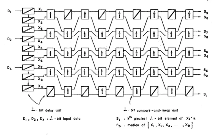
Theodd/even transposition sorting network is a pipelined modularstructure consisting of w compare-and-swap stages [43]. A compare-and-swap stagehas
(w — l)/2, w is odd, full-word (Z-bit) parallel compare-and-swap units and an Z-bit delay unit to delay the window element which is not compared at that stage. Each compare-and-swap unit operate on the odd and even pairs
of the window elements alternately (Fig. 3.1). Odd pairs are in the form of (Xn,Xn+i) where n is odd, whereas n is even for even pairs. Each Z-bit
compare-and-swap unit compares the two Z-bit elements at its inputs and
interchanges them if necessary so that the larger one of the elements will
be at the “top” and the smaller one will be at the “bottom” output. At the output of the last stage, the input elements will be sorted such that the largest will be at the “top” and the median will be at the middle.
If the odd/even transposition network described above is implemented in
hardwareas a single chip median filter for afixedwindow size, w0, then one cannot use that chip tofind the exact medians of the window elements that
is larger than w0. On the other hand, there is no flexibility on the word length because the compare-and-swap unit can be implemented only for a
fixed word-length inthis configuration. Furthermore, the compare-and-swap
unit can complete itsjob after an Z-bit comparison resulting ina large prop agation delay. Although, the throughputof the networkis one Z-bit median
D| , D2 , D3 > J- - bit input data Sk : k,h greatest X- - bit element of Xi ' s. Sg î median of | X| f Xg, Xg,... , Xg I
Figure 3.1: The ordinary odd/even transposition network (w = 9).
per clock (assuming a sequential logic implementation), it is not possible to clock this network with a frequency required forthe real-time operation rate
sincethe clock period will be at least the time required for a full-word com
parison. All these results show that the odd/even transposition network in
the configuration described above can not satisfy any of the requirements
for a general purpose median filter {extensibility in window size, unlimited.
word-length, and real-time application capability).
However, the odd/even transposition network can be modified so that
resultant structure(s) can satisfy our needs. Starting from this approach, two median filter networks are obtained. Both of these networks are bit
level, systolic and pipelined odd/even transposition sorting networks that employ all the advantages of the systolic algorithms and satisfy the fisted
requirementsfor a general purpose median filter. The networks serve different
purposes: one of them designed for unlimited word-length and extensibility to larger window sizes whereas the other one is for real-time applications.
3.2
Extensible
Median
Filter
Network
The odd/even transposition network shown in Fig. 3.1 is modified such that
every operation is in the bit-serial form. We have used a bitwise compare- and-swap unit so that data flow is reduced to flowing of bit streams which eliminates the limit on the word-length and the large delay due to full-word
comparison. In addition,the replacement of the delay units by the
compare-and-swap units comeup with extensibility in the windowsize. In the following
paragraphs, the resultant extensible network is described in detail.
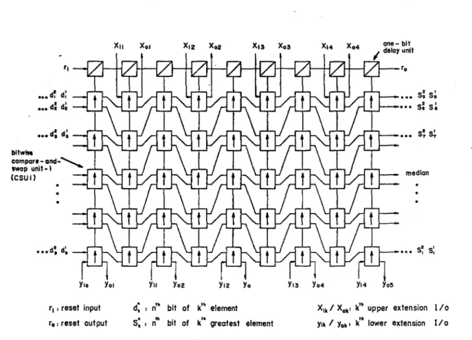
The extensible odd/even transposition sorting network is a pipelined sys
tolic structure consisting of w = 9 compare-and-swap stagesthat operate on
the consecutive pairs of window elements alternately. A compare-and-swap
stage consists of(W + l)/2 bitwise compare-and-swap units. Each of these units compares the two one-bitnumbers at its inputs and interchanges them
if necessary so that the larger one is at the “top”. At the output of the last
stage, the data will be sorted such that the largest will be at the “top”, and the median will be at the middle.
At each clock, one bitfromeach word (total of w bits) entersthe network
and one bit of the median is obtained at the output. The flow is from the most significant bits toward the least significant bits both at the input and the output. Due to serial bitwise data flow, this structure allows arbitrary word-length, L. The network is given in Fig. 3.2 for W = 9.
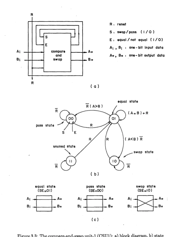
The bitwise compare-and-swap unit, CSU1, has two one-bit data inputs
Ai and Bi, a reset input R, and two one-bit data outputs Ao and Bo. It
also has two internal parameters S (1/0: swap/pass) andE (1/0: equal/not equal) which are updated and stored in the CSU1 (Fig. 3.3). Because of the feedbacks S and E, the best structurefor the CSU1 is afinite state machine
to have a reliable timing [46]. The CSU1 compares Ai and Bi, and either passes them unaltered, or swaps them. It has three legal operation states:
equal state , pass state and swap state. The present state values of S and E shows the subresult of the bitwise comparison of the more significant bits whilethe next state values indicate the new subresult.
CSU1 is set to the equal state (S = 0, E = 1) by the reset signal R at
the beginning of each computation cycle. This is the instant after the least
significant bit of theprevious cycle leaves and before themost significant bit of the next cycle enters the CSU1. Thus the reset signal also flows through
T| > reset input di s n‘ bit of k’h element
r0: reset output Si i n" bit of k’“ greatest element
Xik/Xok: k1" upper extension l/o yik f y0»‘ k'" lower extension I/o
Figure 3.2: The extensible median filternetwork (w = 9).
the stages of the network. Forthis purpose, a chainof the bitwise delay units are used to reset the stages at appropriate time instants (see Fig. 3.2).
Duringthe computation, the CSU1 staysin the equalstate (S' = 0, E = 1)
and passes the input data unaltered (Ao = Ai and Bo = Bi) as long as the twoinput bits are equal as they flow in. However, it locks itself into the pass
state whenit first findsthat Ai >Bi and passes the inputs unaltered. On the
other hand, it locks itself into the swapstate when it first finds that A, < Bi
and swaps the inputs, Ao —Bi and Bo — Ai.
The extension I/O’s (^¿/o’s and yi/o's, see Fig. 3.2) of the extensible
median filter network areused toextendthe filter to the window sizes larger than w = 9. If the upper and lower extension inputs (ar,’s and y,-’s) are connected to logic l’s and 0’s, respectively, so the corresponding CSUl’s
operate as delay units. This is due to fact that the CSU1 will always pass the inputs unaltered if its inputs are IX orX0 ( A,- = 1 ,Bi = Xor A,; = X,Bi = 0),
where X indicates don’t care (i.e, X may be 1 or 0). On the other hand, if
the network given in Fig. 3.2 is used as an array element to find the exact
R
R : reset
S -. swop / pass ( I / 0 ) E : equal / not equal ( I / 0) Aj , Bj : one-bit input data Ao, Bo : one-bit output data
( a) equal state (SE=OI) pass state (SE=OO) swap state (SE=IO) Bi Aj Ao Bo
Figure3.3: The compare-and-swap unit-1 (CSU1): a) blockdiagram,b) state diagram, c) operations.
Figure 3.4: Interconnections of the extensible median filter networks for
w = 9.
then these CSUl’s operate as usual except those corresponding to the upper
extension I/O’s of the upper most network and corresponding to the lower
extension I/O’s ofthe lowest network. In this case, the CSUl’s corresponding
to the interconnected extension I/O’s of the networks are not forced to lock in one state by means of extension signals, but they are free to enter any
state dependingon their inputs. As a result, the extensibility to indefinitely large windows is achieved: in the normal mode, it is possible to compute
the exact median of a group of 9 elements using only one network, and for
groups of w elements where w > 9, at most [w/9]2 ([.] indicates the smallest greater integer) networks areneeded with appropriate interconnections of the extensionand data I/O’s similar to the connection scheme in Fig. 3.4.
The extensible network described above generates its outputs with a pipeline delayof w+L clocksand after the network is full, it finds one median
per L clocks. The network can operate at a clock rate that is determinedby
the delay ofone compare-and-swapunit which consistsof, at least, the delay of a few cascaded bitwise comparisons and a 2 X 1 multiplexing. Although, the resulting speed can be sufficient for the real-time median filtering of the
512 x 512frames with L < 5, it is less than the real-time operation rate for
3.3
Real-Time
Median Filter
Network
In orderto achieve a real-time operating rate for the 1024 x 1024 resolution
frames, the only way is to find a structure that has a very high throughput
capability. The only solution we have found is the odd/even transposition
sorting network configuration proposed by Oflazer [48]. In thefollowing sec tion,we will describe the real-time median filter network designed for w = 9 and L = 8 which is a variation of Oflazer’s network that was designed for
w= 5 and L= 8.
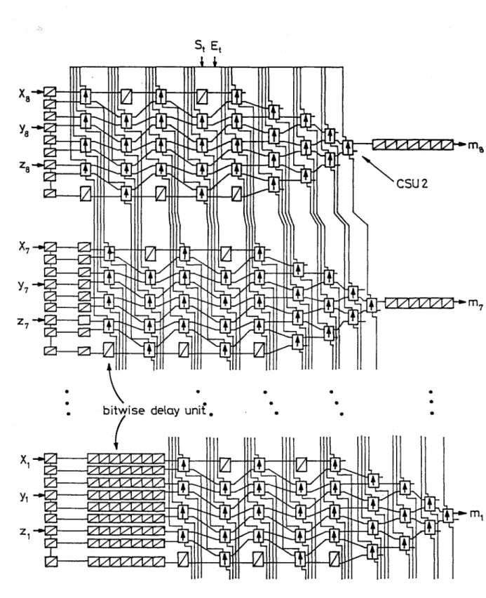
A median filter with very high throughput can be designed by intercon
necting L number of the pipelined odd/even transposition sorter blocks in
parallel and applying the systolic concepts at the bit-level. The block dia
gram of the overall network for w — 9 and L = 8 is shown in Fig. 3.5. In this network, the data enter in such a way that the most significant bits go
to the first block, the second most significant bits to the second block and
so on. There are nine 8-bit input data, and one 8-bit median is obtained per clock. At every clock, three new elements enter the network, corresponding to the new elements ofa sliding 3x3 window.
The bitwise compare-and-swap unit, CSU2, used inthis networkis slightly
different from CSU1 in sucha way that the S andE parametersof CSU1 are external parameters in CSU2. These parameters are taken as inputs Si and
Ei (the cumulative subresultof the bitwise comparison of the more significant
bits) from the upper block, used, updated and sent out as So and Eo (the
new cumulative subresult) to the lower block. Hence, CSU2 does not have
any storageorthe reset input signal. The functional description of CSU2 is given in Fig. 3.6.
During the computation, CSU2 compares the inputs Ai andBi and passes or swaps them conditionally depending on Si and E{. IfEi = 1 and Si = 0, it passes or swaps the inputs so that larger one goes to Ao and the smaller
to the Bo. On the other hand, if Ei = 0 and Si = 1, CSU2 passes/swaps
the inputs independent tothe result ofthe comparisonof the inputs. It also
updates Si and Ei and sends out as So and Eo for the comparison of the less
significant bits.
The computation at each stage of a lower block starts after the corre
sponding stage of the upper neighborhood block completes its operation so that the S/s and Efs are ready at input of that stage. As a result of this,
St Et
I
I
Xj.yj.Zj : ith bits of the inputs corresponding the new elements in a
3x3 sliding window.
mi : ith bit of the median
St,Et : Test inputs for testing of the blocks individually.
So Eo
Sj and Ej indicate the
S
q = Si + Ej ( Aj < Bj ) Eo= Ej ( A, = Bj )Ao = if So then Bj else Aj
Bo = if Sothen Aj else Bj
cumulative subresult
comparison of more significant bits while Eo
of the bitwise
and So indicate
the new cumulative subresult.
Figure 3.6: The compare-and-swap unit-2 (CSU2).
each stage of a lower block must operate one clock later compared to the corresponding stageof the upper block. For the samereason, the outputs of
a lower block are readyone clock later compared to the upper neighborhood
block. In order to employ a proper timing,the pipeline delay units are used
both at the input and the output of the network such that k’th block from
top has (k— 1) delay units at its inputs and (Z — k) delay units at its output, where k = 1,2, ...L (see Fig. 3.5).
The throughput of the network is one full-word median per clock. The clock periodis determined by the delay of one CSU2. Recent VLSItechnology
allows the implementation ofCSU2 at a speed larger than the real-time rate for the 1024 x 1024 frameswith L = 8.
3.4
Feasibility
of
VLSI
Implementation
Bothof the extensible and real-time median filter networks areregulararrays
of bitwise compare-and-swap anddelay units. Also, their internal communi cation schemesare simple andregular. Thismakes the VLSI implementations to be easy and straightforward. Furthermore, the testing of the VLSI chip
may be easily accomplished by the functional test techniques [51], since the
operations of the cells may be selectivelyprobed by issuing proper test vec tors. The testingoperation includes the runningof the chip with test vectors as inputs andthe comparison of the outputs with expected results. Thetest ing can be performed on-line or off-line, in any case, the comparison time
is reasonably short. The generation of the expected results, which are the correct outputs, can be obtained by using a software sorter and a software medianfilter.
The extensible median filter chip can be tested by using a few hundreds test vectors. If we apply the same element to all of the inputs, then every
CSU1 willact in equal state. On the other hand,the sorted inputs will cause
all the CSUl’s operating inswap state. Consequently, a set of inputs sorted
in reverse order will make all the CSUl’s operatein swap state. By this way the CSUl’s will be tested in all the operation states.
The real-time medianfilter chip can betested by using 12,288(8 x 3 x 29)
test vectors. The Si’s and E^s at the top of the network are connected to external test control inputs, St and Et respectively (see Fig. 3.5). These
test control signals are usedto isolate theoperation ofeach blockfrom each
others,thus the numberof test vectors reduced to 12,288. If these testinputs are not used then thenumber of test vectors willbe afew millions. The k’th
block can be tested individually with applying logic 1 to all of the upper blocks’ inputs so that it receives the external St and Et without any change.
As a result, each block can betested by using 1,536 (3 x 29) test vectors: all
combinationsof one-bit 9inputs times 3, where 3 comes from the legal values
of the pair S{E{ (01, 00, 10).
The extensible network can be implemented with about 5 K transistors and packaged in 28 pins with 2x1 I/O multiplexing whereas the real-time
medianfilter will consist of about 20 K transistors and has 40 pins.
One may chooseto implement either theextensible median filter network orthe real-time network for a large w, but this not preferable since the area is proportional to w2. We have chosenw = 9, because it isthe minimum and
the most commonly used window size in two-dimensional median filtering
applications.
In an attempt to increase the efficiency of the silicon area use, onemay consider to design a network which utilizes the samecompare-and-swap units (CSU1 and CSU2) in both modes by altering the interconnections via the ex
ternal select signal. Examination of this possibility didnot give the desired
result: the chip area turned out to be larger because of the decreased regu
larity and increasedinterconnections.
We have examined a network with real-time and unlimited word-length
such that all of the Si and Ei inputs of the upper most sorting block and So
and Eo outputs of the lowest block are used as extension I/O’s. But VLSI
implementation of this network needs an extremely large number of I/O’s and unfortunately there is no way tomultiplex such a fast network I/O’s without decreasing the speed. Hence, it is not feasible and wehave not attempted to
implement it.
We have also examined the implementation of the two networks in the
same chip. The I/O’s of the two networks need to be multiplexed. On the
other hand, due to very long wiring paths from I/O pads to the networks’
I/O’s, the strong buffers areneededto drive the largewiring capacitive loads. All these increase the area and decrease the throughput of the networks re sulting a reduced speed which makes the real-time operation critical. Also,
whileone of the networks operatesthe other one can not be used due tomul tiplexed I/O’s, i.e. oneof the networks willbeidle at all times. However, the implementation of the networks as two single-chipswill avoid these undesired results.
4. VLSI DESIGN METHODOLOGY
4.1 VLSI
Design
Approach
For the design of any kind of systems, a systematic approach is necessary; es pecially for the design of complex andlarge systems, the systematic approach becomesvery important. For design of a chip, startingfrom the problemdef
inition, a systematic wayshouldbe followed throughout the design steps. For system design in VLSI, there are someproposed approaches in the literature [21,46,52]. In fact, all approaches are based on dividing the task into four
main subtasks which are the problem specification, behavioral description,
circuit description, and layout description. The problem specification con
sists of the detailed definition ofthe problem and well defined constraints. The behavioral description is the algorithm found as the solutionof the prob
lem whereas the circuit and layout descriptions are the implementations of
the algorithm in circuit and layout levels. Further divisions of those main subtasks, and their orders depend on the application and probably on the designer.
For our design, the two mainsubtasks, the problem specification andthe
behavioral description, aregiven in the previous chapters. Our problem is to
design and implement a general purpose medianfilter which has the exten
sibility, unlimited word length and real-time operation capability. We have a solution to that problem in the form of two median filter algorithms that satisfy the constraints. The algorithms are described in terms of the net work block diagram representations with functional descriptions. A testing
strategy is also determined in that step. All thesecomplete the two main sub
tasks. Now, the remainingparts are the circuit and layout implementations.
Since our networks are modular and have regular and simple communication
schemes, it is quite easy to divide the circuit and layout implementation in
unit, delay unit, and I/O cells) instead of designing the full network at a
time. Obviously, the same partitioning canbeperformed in the layout level. All thesepoint out the importanceof the structured algorithms (e.g. systolic algorithms) since the complexity and difficulty of the tasks at circuit and layout levels are determined by the algorithm.
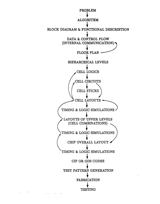
The flow chartgiveninFig. 4.1 shows the all steps which we have followed
throughout the designof the extensible and the real-time median filterchips. After completing the problem andbehavioraldescriptionparts, it is essential to construct a floor plan for the chip. The floor plan at this step is not necessarily strict but it is rather flexible for modifications in layout steps.
The floorplan strongly depends on the structure of the algorithm, especially on the data flow and controlflow of the algorithm. The determination of the hierarchical levels is to classify the groups of the cells and combinations of them level by level such that the lowestlevel consists ofprobably the smallest cells and the second level has the units that are the combinations of a number
of subcells andso on. Obviously, the top level in the hierarchy is the overall chip.
The next step in the approach is the logic design of cells. If the cells are standard gates or consisting of a few them, then the logic expressions of
the cell parameters and their representations in terms of gates need to be determined so that, in the circuit design, the only task will be to replace
the gates with their known equivalent circuits. However, if the cells consist
of ratherlarge number of gates, then the cell parameters must be expressed as logical functions but the gate representation is not essential because the circuit implementations in transistor level of such cells may be simplerthan doing that ingate level. The designer must consider the testingof the chip at
this step so that the extra logic circuits are included for testing if necessary.
For the circuit implementation ofcells, the designer should choose a cir
cuit design technique in a particular technology (e.g, NMOSor CMOS) which
showsthe best performance for his application. Each technology offers some circuit techniques employing different properties. The performance of the
technologies and circuit techniques vary depending on the design criteria. For example, CMOSis preferable for the designs requiring a low power con sumption. We will discuss the selectionof a suitablecircuit design technique
PROBLEM
I
ALGORITHM
I
BLOCK DIAGRAM & FUNCTIONAL DESCRIBTION
I
DATA & CONTROL FLOW (INTERNAL COMMUNICATION)^
i
y
FLOORPLAN---I
HIERARCHICAL LEVELS CELL CIRCUITS CELL STICKS CELL LOGICS CELL LAYOUTSTIMING & LOGIC SIMULATIONS LAYOUTS OF UPPER LEVELS
(CELL COMBINATIONS) TIMING & LOGIC SIMULATIONS
CHIP OVERALL LAYOUT TIMING & LOGIC SIMULATIONS
CIF OR GDS CODES TEST PATTERN GENERATION
I
FABRICATION TESTING
The cell circuits can be mapped into layout either directly or after rep
resenting them in stick forms. For a well organized layout, the sticks may
be helpful especially to match the constructed floor plan. But in general, the circuits canbe directly converted to layout forms by experience. In any
way, during the generation ofcelllayouts, one should care about the physical behavior of the layout (transistor sizes, the resistive and capacitive effects, coupling, etc.). Furthermore, the cell boundaries for cell combinations, the data and control flow between them, and the floorplan must be also consid
ered.
After the generation of cell layouts, the next step is the simulation. The circuits corresponding to the layouts are first extracted and then simulated byusing software simulators. The simulation can beperformed in two steps: timing analysis and logic analysis. But these two steps can be handled in a
single step if there are a few cell parameters. For example, an OR gate can be simulated in a single step, since the parameters are two or three inputs and one output, so that the timing analysiscan include also the logic test. If there are reasonably manycell parameters, timing andlogic simulations must
be performed separately by a timing simulator and a logic simulator, since the logic test with timing simulator will be costly in terms of simulator run time. Accordingto our experience, the mostly used feedback loop is the cell simulations to celllayouts because the most of the optimizations (speed, area, power, etc.) are performed at the cell level since it is the lowest hierarchical level.
After the cell layouts, the following design step is the layouts of upper hierarchical levels. The simulation at these levels are not essential because
all subcells are simulated at the lowest (or lower) level. But if the designer
worries about the operation of cells when they are combined, he must per form the necessary simulations. However, if the simulations at lower levels
are performed with consideration of the combinations (e.g., some extra ca
pacitances may be need to add to the output capacitances of the cell being simulated), simulations at upper levels are not necessary.
As a last step of the layout level, the overall chip layout is obtained including the I/O cells(buffers, paddrivers, pads, etc.) Finally, atiming and a logic simulation of the chip must be performed. If the simulator run-time
is feasible, the logic simulation can be performed by using the test vectors
number of test vectors is too large so that the simulation by using them is not possible. In fact, since all the voltages and currents within the chip
are observable in the simulation,the simulation with test vectors are not so
essential. Consequently, if the test vectors will be used in the simulations, they are generated at that step.
The last two tasks are the generation of the CIF or GDS-II codes and the test patterns (test vectors). The CIF or GDS-II codes are generated by the layout editor automatically. The test vectors can be obtained by either atest pattern generator or manually. In general, the test vectors are generatedmanually since a general purpose test pattern generator is a very
expensive tool. However, one can write a software program to generate the
test vectors for his own purpose. The chip testing can be performed either by the manufacturer or by the designer. If the chip will be tested by the manufacturer, the test vectors must begenerated before the fabrication.
4.2
Circuit
Technique
In integrated circuit design, especially for digital applications, NMOS tech
nology has been used with a growing potential since early of 1960’s. Due to
the increase in density of devices on chips, the power dissipation and com
plexityof chipshavebecomeaseriousproblem. Since the late 1960’s, CMOS
technologyis being usedto overcomethese problems bypossessing a reason
able low power consumption, a rather easy design and a comparable speed
with NMOS [55]. Also, the noiseimmunity of the CMOS is better than that
of NMOS. Forthese reasons, we have implemented the median filter chips in
CMOS technology. In particular, it is a 3-micron double metal double poly n-well process.
During the implementation of circuits in CMOS, one should consider
the latchup, the charge sharing, the body effect, and the noise margins.
[46,56,53,54]. Note that, these problems except the latchup are also present in circuits implemented in any technology (e.g. NMOS).
Thelatchupproblem is caused by the improperlybiasedparasiticbipolar
transistors formed within the CMOS structure. In some cases, these parasitic transistors are biased in such a way that Vdd and Vss (positive and negative
powersources)areshorted resulting in destructionofthe chip due to excessive
transistors so that they do not cause to the short circuit. In practice, one can reduce the chances of the latchup in n-well CMOS by a proper number of connections from the p-substrate to Vdd and from the n-well to Vss, and increasingthe distance between n-well and n-diffusion.
If the output capacitance of a subcircuit, say a gate, is not comparable with the load capacitance (sum of input capacitances of the gates derivedby
that gate) then a charge sharingoccurs between the capacitances resulting in that the output voltage of the gate oscillates before settling in its final value.
On the other hand, the asynchronized inputs ofa gate can causethe charge sharing at theoutput of the gate. In other words,the chargesharing creates some glitches which may cause wrong logical output. However, the charge
sharingproblem can be avoidedby makingthe output capacitance and load
capacitance to be comparable, and synchronizing the input signalsby means ofweak buffers.
If the source voltage of a p/n-transistor is not equal to Vdd/Vss, then the threshold voltage of that transistor changes depending on the source voltage since the threshold voltage is a function of the source to substrate
voltage. Inmany circuits,some transistorsarecascodedso that the source of
every transistor is not connected to Vss. This causes the change of expected
results especially in timing, due to the body effect. The only precaution for
that problem is to increase the Vssconnections, and to decreasethe internal
node capacitances as much as possible. Furthermore, in timing simulations,
a worst case approach is essential.
Thenoisemarginparameter is ameasureofallowable noise voltageon the
inputof a circuitsuch thatthe output is not affected. Ingeneral the highand low noise margins are equalized by the equal low and high going transition
times. Also, the selectionof the logic style is important tomaximize the noise margins.
In CMOS technology, there are some circuit implementation techniques
called logic styles. These arecomplementary (standard) CMOS logic, pseudo
NMOS logic, dynamic CMOS logic, clocked CMOS logic, CMOS domino logic, cascade voltage switch logic (CSVL),and pass transistor logic [46,53,54]. Each logic style possesses some different properties. In other words, the
optimization of the cost function (speed, area, power, complexity, etc.) is
different. For example, dynamic CMOS logic is the choice for fast circuits but its timingis critical. Hence, the designer must choose the best style for
his particular application. In our design, the standard CMOS logic style is used since this logic style possesses a more reliable timing, a rather easier
mapping in layout, a lowerpower consumption, and a better noise immunity comparedto the other styles. Furthermore, its areaand speed performances
are comparable with the otherstyles.
4.3 VLSI Tools
At the layout stepof aVLSI design, it is necessary to use somesoftwaretools inordertoedit the layout of achipwhich consists of thousandsof transistors,
and to perform itssimulations. In our design, we have used the Berkeley CAD Tools of University of California and VLSI Tools of University of Washington
[57,58] running under the Unix operating system on SUN workstations. For
editing of layouts, we have used MAGIC which is an interactiveeditor that
can make on-line design rule check by using information in the design rule file. Thus the designer must provide the design rules that are prescribed
by the manufacturer. Unfortunately, MAGIC can not realign the symbolic layers if the design rule file is changed, so the layout must be reedited or
modified accordingto the new design rules. MAGIC allowsediting the layouts hierarchically, and extracting the circuit of the layout.
In order to perform simulation of a cell, first the circuit of the cell is ex
tracted, andthen it is further processed by some intermediate tools [57,58].
There are three simulators: SPICE, RNL, and ESIM. SPICE can be used for the timing simulations with a high accuracy. Before running SPICE,
extracted circuit must beprocessed by EXT2SIM and SIM2SPICE tools to convert the extracted circuit to SPICE format. In addition, the model pa rametersof the transistors, and thetiming commands should be entered into
the SPICE input file. The results of SPICE simulations are either observed on the screen by using SPCVIEW and SPICE2SUMMARY tools or plotted by SPCPLOT tool. RNLis used forlogic simulations with approximatetim
ing. In order to use RNL, extracted circuit is processed by PRESIM. If RNL is used in interactive mode, the control and timing commands are entered
interactively, otherwise RNL needs a control file consisting of control com
mands, and a time commands file consistingof input signals ordered in time.
One can use GEN-TIME and GEN_CONTROL to generate the control and
only combinational circuits, but it is very fast since it performs switch-level
simulation. The results of simulations with RNL and ESIM are stored in ordinary files, thus user canread and analyzethe results from these files.
After completing the layout editing and simulation tasks, thefinal layout is converted to CIF or GDS-II codes by using MAGIC. These codes are used
togenerate the masks of the layersforfabricationof the chip. If it is required,
one can plot themasks from codesby using CIFPLOT tool, and convert the codes back to layout format by usingMAGIC.
5. VLSI IMPLEMENTATION
5.1
Implementation
of the Extensible Median
Filter
In the description of the algorithm of the extensible median filter, it is pro posed to multiplex the I/O’s of the extensible median filter chip to reduce the
pinnumber from 40 to 28. However, in the layoutimplementation of the chip, it is observed that there is no increase in the area when 40 pads are used.
This is due to fact that there are empty spaces between the pads when the
28 pads are placed. For this reason, we have used 40 pads in the extensible
median filter chip. Since there is no multiplexingin this case, the speed of the chip is increased by about 30 percent, and the data loading and reading operations are simplified. The only disadvantage is increasedpackage size in
the case of “dip” package. In this section, the implementation of the 40 pin extensible median filter chip with no multiplexing is described. Here, let’s
point that one can easily add multiplexers around the network and reduce the pin numberto 28.
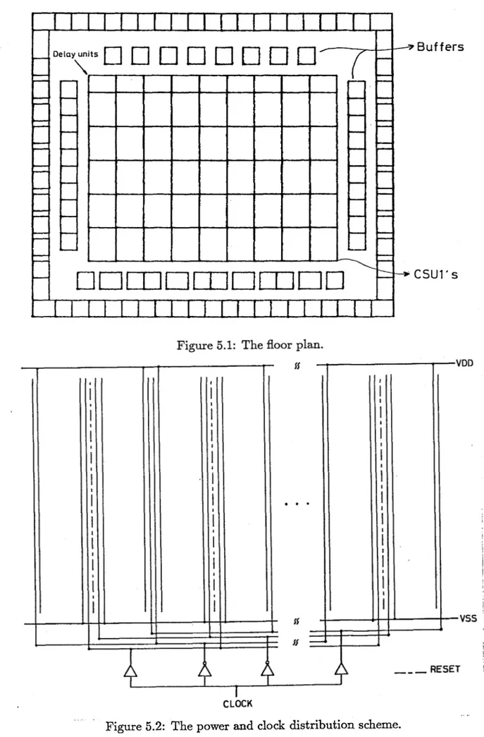
As the first step, the floor plan of the chip is designed (Fig. 5.1). Then,
the power distribution schemeof the chip is determined. A clock distribution scheme is selected such that the lengths of the paths that the clock signals
propagate are equal and small enough so that the clock skewis not aserious problem. Hence, a single clock buffer is used for each clock phase, insteadof a distributed clock buffering scheme [59]. The power and clock distribution
scheme is shown in Fig. 5.2.
In the following subsections, logic expression(s), the circuit and layout
descriptions, and the timing and/or logic simulations will be described for
each unit of the chip. The complete layout and the logic simulation results
of the chip will be given. Finally, an overview of the chip and its testing will
5.1.1
Compare-and-Swap
Unit-1 (CSU1)
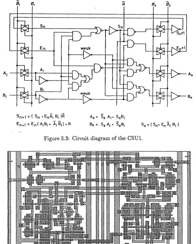
The logicexpressions of the CSU1 are obtained from the state diagramgiven
in Fig. 3.3. Theyareminimized byusing thecarnough-mapmethod [60]. The
resultant logic expressions and the circuit diagram of the CSU1 are given in Fig. 5.3. In this circuit, inputs enter the cell during = 1, (j>~ = 0). The
computation of the outputs starts as soon as the inputs are latched. When the outputs are computed, they are latched at the outputs of the inverters
during <f>~. In the circuit, the weak buffers are used to prevent the charge sharing. Theinverters at the output of the circuit are necessary to latch the
outputs. Theseinverters are dynamic latches so they can not hold data more than about 1 millisecond without refreshing [21]. This meansthat the clock frequency can not be less than 1 KHz.
The circuit of the CSU1 is converted to the layout by consideringits ge ometry in thefloor plan. After the equivalent circuitof the layout is extracted
and simulated, the layout is modified to increase the speed, to prevent the
charge sharing and to have equal rise and fall times by resizing the proper transistors. The maximumaverage current is about 0.7mA. The powerfines of the layout arewide enough so that the metal migration does not takeplace
(the allowable maximum current density of each layer is determined by the
manufacturer). The final form of the layout of the CSU1 is shown in Fig.
5.4. This layout consistsof 39 p-channel and 39 n-channeltransistors.
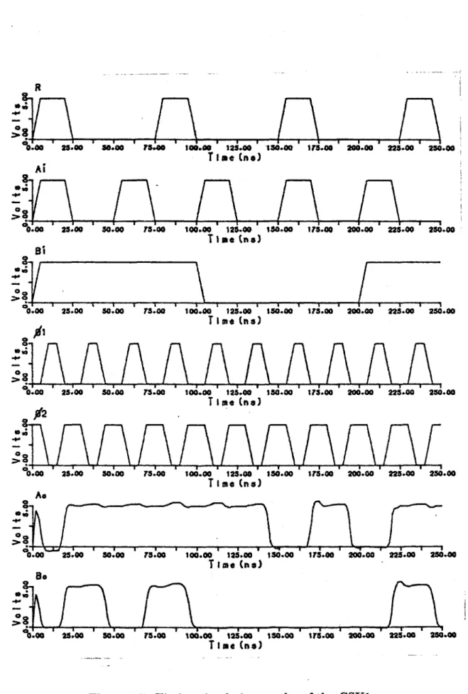
The timing simulations of the CSU1 are performed with different clock
frequencies and with different rise and fall times by using SPICE. Here, we give the input and the output waveforms for 40 MHz clock which is the maximum clock frequency (Fig. 5.5). In these waveforms, the rise and fall
times of the clock, inputs, and outputs are about 5 nsec. However, the rise
and fall times may be larger than 5 nsec for low operation frequencies if it
is desired. The ripples on the waveforms are less than 1 V, thus they are negligible. The logic simulation of the CSU1 is performed by using RNL for
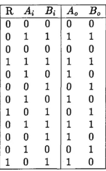
all possible inputs. As an example, the results of the logic simulation for three different 4-bit input words are given in Table. 5.1. For the sake of the
clearness, the clocks and time steps are not shown. As a result, the timing
and the logicsimulations show that the CSU1 with the given layoutfunctions correctly.
Sn+1 = ( Sn ♦ EnAj Bj )R Ao = Sx Aj* SxBj
^n*1 = En ( AjBj ♦ Aj Bj) ♦ R Bo = Sx Aj ♦ SxBj Sx = ( Sn*■ Sn Aj Bj)
Figure 5.3: Circuit diagram of the CSU1.
Bi T l Be (ns) 100.00 123.00 130.00 173.00 200.00 223.00 230.00 T I me (ns) 0.00 23.00 so.oo n.oo MAAAAAAAA 0.00 29.00 - 90.00 -73.00 /2 t00.00 123.00 130.00 173.00 200.00 223.00 230.00 TI me (ns)
iMWWMAAAUM
0.00 29.00--- --- --- -- 90.00 73.00 100.00 123.00 130.00 175.00 --- --- ---200.00 223.00 290.00 T I me (ns) A« Bo S-. SO.OO 73.00 100.00 123.00 130.00 175.00 200.00 223.00 250.00 TI me (ns) 0.00 25.00Table 5.1: Logic simulation results of the CSU1. R Ai Bi Ao Bo 0 0 0 0 0 0 1 1 1 1 0 0 0 0 0 1 1 1 1 1 0 1 0 1 0 0 0 1 0 1 0 1 0 1 0 1 0 1 0 1 0 1 1 1 1 0 0 1 1 0 0 1 0 0 1 1 0 1 1 0
5.1.2
Delay Unit
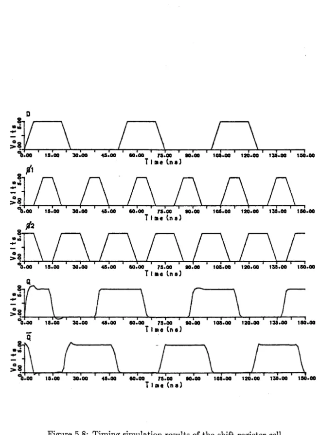
Since the reset signal must propagate through the delay units one stage per cycle, a shift register cell can be used as the delay unit. The static D-type master-slave flip-flop is chosen as the delay unit in order to have a reliable shift operation [60,53]. The circuit diagram and the layout ofthe shiftregister cell are shown in Fig. 5.6 and Fig. 5.7. In this circuit, the input is latched at the output of the master flip-flop during <j> = 1. The master flip-flop is disabled when (/> is low. The input is latched at the output ofthe slave flip
flop during = 1. The output of the master flip-flop is buffered and sent
to the compare-and-swap stage as the complement of the reset signal. The
results of the timing simulations of the cell are given in Fig. 5.8.
5.1.3
Clock Buffers
The total capacitive load of <f> and (f>~ lines are about 15 pF and 20 pF
respectively. Four buffers are used to drive these loads with 100 percent tolerances: two oninverting buffers for and two inverting buffers for .
The noninverting buffercan drivea 15 pF load with the 2.5 nsec rise and fall
times whereas the inverting buffer can drive a 20 pF load with the 2.5 nsec
rise and fall times. In order to minimize thedelay of the buffers, the number of stages and their ratios are calculated [61,20]: the noninvertingbuffer has 4 stages with3.6stage ratio while the inverting buffer has the 5 stageswith 2.9
01 02
( to the compare-and-swap stage)
Figure 5.6: Circuit diagram of theshift register cell.
t11X3*3