M A T E R I A L S S C I E N C E Copyright © 2018 The Authors, some rights reserved; exclusive licensee American Association for the Advancement of Science. No claim to original U.S. Government Works. Distributed under a Creative Commons Attribution NonCommercial License 4.0 (CC BY-NC).
Electrically switchable metadevices via graphene
Osman Balci,1* Nurbek Kakenov,1Ertugrul Karademir,2Sinan Balci,3Semih Cakmakyapan,4 Emre O. Polat,5Humeyra Caglayan,6Ekmel Özbay,1,7Coskun Kocabas1*†
Metamaterials bring subwavelength resonating structures together to overcome the limitations of conventional materials. The realization of active metadevices has been an outstanding challenge that requires electrically reconfigurable components operating over a broad spectrum with a wide dynamic range. However, the existing capability of metamaterials is not sufficient to realize this goal. By integrating passive metamaterials with active graphene devices, we demonstrate a new class of electrically controlled active metadevices working in microwave frequencies. The fabricated active metadevices enable efficient control of both amplitude (>50 dB) and phase (>90°) of electromagnetic waves. In this hybrid system, graphene operates as a tunable Drude metal that controls the radiation of the passive metamaterials. Furthermore, by integrating individually addressable arrays of meta-devices, we demonstrate a new class of spatially varying digital metasurfaces where the local dielectric constant can be reconfigured with applied bias voltages. In addition, we reconfigure resonance frequency of split-ring resonators without changing its amplitude by damping one of the two coupled metasurfaces via graphene. Our approach is general enough to implement various metamaterial systems that could yield new applications ranging from electrically switchable cloaking devices to adaptive camouflage systems.
INTRODUCTION
Metamaterials have been a powerful tool to control and manipulate electromagnetic waves and their interaction with matter (1–3). The in-tegration of passive metamaterials with a variety of tuning mechanisms has been extensively examined to generate active metadevices that have novel functionalities (4–7). Because of the different tuning mechanisms, these active metadevices can be classified into three general categories, which are circuit-, material-, and physical-based metadevices (8). The circuit-based metadevices use variable capacitors or switches to alter the lumped elements of the equivalent circuit. For instance, the reverse bias voltage applied on a varactor integrated on a split-ring resonator (SRR) changes the effective capacitance of the equivalent circuit (9–12). Material-based metadevices rely on controlling bulk material proper-ties, such as the permittivity, permeability, or conductivity, of the indi-vidual unit cell under an external stimulus (7, 13–18). The conductivity of semiconducting material deposited in the split gap can be tuned by illumination and thereby alters the resonance frequency of the meta-material. Similarly, interconnected metamaterials fabricated on a semi-conductor surface have been used to control the depletion area that alters the free-carrier absorption (19, 20). Alternatively, some phase transition materials, such as VO2, have been used for altering the resonance behavior of metamaterials (21, 22). By changing the tem-perature of these materials around the phase transition temtem-peratures, one can control their conductivity and hence the resonance behavior of metamaterials made of or integrated with them. On the other hand, physical metadevices tune their response by changing their shape or
relative position of subcomponents (such as split gap) (23–27). For ex-ample, microelectromechanical-based devices can modify the resonance frequency of metadevices in terahertz spectra (25). Although the demon-strated devices provide some degree of tunability, their performances are limited to narrow spectra with a small dynamic range due to the material and fabrication limitations. Therefore, these technologies would greatly benefit from a material that yields large tunability over broad spectra. None of the existing materials provides these challenging requirements. Furthermore, the requirement for electrically controlled tunability places another challenge for practical applications of metadevices.
Two-dimensional (2D) crystals provide new perspectives for re-configurable smart surfaces that can be used for the realization of elec-trically tunable metadevices (28–32). The thickness of 2D crystals is much shorter than the effective wavelength; therefore, their electro-magnetic response solely originates from the charge carriers. Recent studies have shown that tuning the density of high-mobility free carriers on graphene yields an unprecedented ability to control light-matter interaction over a very broad spectrum ranging from visible to microwave frequencies (33, 34). By engineering the shape or doping level, the plasma frequency of graphene can be tuned between infrared (IR) and tera-hertz frequencies (30, 35). Notably, the charge density alters the effective dielectric constant of the medium. In another approach, graphene is coated on metamaterials (36, 37) or optical antennas (38, 39) to yield electrically tunable metadevices. However, these devices are not suitable for practical applications due to limited tunability (40). Recently, we discovered a simple device structure consisting of an electrolyte medium sandwiched between two large-area graphene electrodes. This geometry permits an efficient mutual gating between two graphene electrodes that
yields charge densities on the order of 1014cm−2(41). Using this
supercapacitor structure, we fabricated various optoelectronic devices, including optical modulators (41, 42), electrochromic devices (43), and switchable radar-absorbing surfaces (44). Here, by using graphene supercapacitors incorporated with metallic SRRs, we demonstrated a new type of electrically tunable metadevices. The fabricated metadevices are based on gate-tunable high-mobility free carriers on graphene, which introduces electrically tunable dissipation in the resonator capac-itively coupled to the graphene electrodes.
1Department of Physics, Bilkent University, 06800 Ankara, Turkey.2School of Physics and Centre for Research on Adaptive Nanostructures and Nanodevices, Trinity College Dublin, College Green, Dublin 2, Ireland.3Department of Photonics, Izmir Institute of Technology, 35430 Izmir, Turkey.4Electrical Engineering Depart-ment, University of California, Los Angeles, Los Angeles, CA 90095, USA.5ICFO– Institut de Ciencies Fotoniques, The Barcelona Institute of Science and Technology, 08860 Castelldefels, Barcelona, Spain.6Laboratory of Photonics, Tampere University of Technology, 33720 Tampere, Finland.7Nanotechnology Research Center–NANOTAM, Bilkent University, 06800 Ankara, Turkey.
*Corresponding author. Email: [email protected] (O.B.); [email protected] (C.K.)
†Present address: School of Materials, University of Manchester, M13 9PL Man-chester, UK.
on February 25, 2019
http://advances.sciencemag.org/
RESULTS
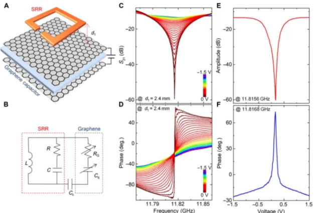
Integrating SRRs in close proximity to graphene surface yields a new type of hybrid metamaterial whose resonance amplitude can be tuned by various means. Previous attempts to integrate graphene with meta-materials yielded very limited modulation in IR and terahertz frequen-cies (35, 37). Here, we follow a different approach by using microwave metamaterials capacitively coupled to a large-area graphene that yields substantial tunability. Figure 1A shows a schematic drawing of this hybrid structure. The presence of graphene in close proximity to SRR introduces additional electrical losses due to the sheet resistance of graphene. The equivalent small-signal model of the hybrid structure is shown in Fig. 1B. The ring and split gap provide the inductance, L, and the capacitance, C, respectively. The resistor, R, models the dissipation on the metal due to the electrical and radiation resistance. In our design,
the SRR is capacitively coupled to graphene (Cc¼ee0
d, where the
cou-pling capacitance,e, is the dielectric constant of the medium and e0is
the free-space permittivity). The graphene layer can be modeled by the
sheet resistance [RG¼ 1
sðnÞ, wheres(n) is a charge-dependent sheet
con-ductance of graphene], and quantum capacitance of the graphene
elec-trodes (CQ¼2e2 ħvF ffiffi n p p
, where e is the elementary charge, vFis the Fermi
velocity, and n is the charge density). The quantum capacitance of
un-intentionally doped graphene layer (CQ~ 0.5mF/cm2) is much larger
than the serial coupling capacitance (Cc~ 5 pF/cm2) and therefore, in
the small-signal model, we can neglect its contribution (45). Capacitive coupling of a graphene layer to an SRR alters the required total imped-ance to achieve a resonimped-ance in transmitting electromagnetic waves.
Therefore, both the capacitive coupling distance (d1) and the charge density (or bias voltage) on graphene change the resonance condition. To tune the electrical resonance of metamaterials, we varied the charge density on graphene layer via ionic gating. It should be empha-sized here that the technical challenge for graphene-based microwave devices is the requirement of large-area devices owing to the
centimeter-scale wavelength (that is,l = 3 cm at 10 GHz). To overcome this
chal-lenge, we synthesized large-area graphene by chemical vapor deposition (CVD) on copper foils, which enables us to realize the proposed micro-wave metadevices (46). Graphene electrodes were synthesized on copper foils using a CVD system, and we subsequently transferred them onto flexible polyvinyl chloride (PVC) substrates by using hot lamina-tion technique. Next, we etched the laminated copper foils in a 5 mM
FeCl3aqueous solution. Although CVD synthesis of graphene enables
the growth of large-area graphene layers, the quality of graphene may diminish because of the inevitable defects and polymeric residues after the transfer. To fabricate graphene capacitor, we first put a paper tissue
with a thickness of 80mm between two graphene electrodes as a spacer
layer, and then we soaked ionic liquid (1-butyl-3-methylimidazolium hexafluorophosphate) into the tissue. The fabricated device structure resembles the supercapacitors formed by single-layer graphene elec-trodes. The used electrolyte permits mutual electrolyte gating between the graphene electrodes without using any metallic gate electrodes. Under an external bias voltage, the electrolyte is polarized and gates the graphene electrodes. The graphene electrode connected to the negative voltage becomes electron-doped (n-doped), whereas the other one
Fig. 1. Electrically tunable metadevices. (A) Schematic representation of the hybrid metamaterial system consisting of SRR capacitively coupled to the graphene electrodes. The capacitive coupling is defined by the SRR-graphene separation, d1. (B) Small-signal equivalent circuit model of the metadevice. SRR is represented by the L, R, and C lump circuit elements; the graphene layer is modeled by the variable sheet resistance, RG, and quantum capacitance, CQ. Ccmodels the capacitive coupling. (C and D) Spectra of the magnitude and phase of the transmittance (S21) at various bias voltages. The color bar shows the bias voltage. (E and F) The variation of the amplitude and phase of the transmittance with the bias voltage.
on February 25, 2019
http://advances.sciencemag.org/
becomes hole-doped (p-doped). At 0 V, the sheet resistance of un-doped graphene is around 2.5 kilohm and it decreases to 0.7 kilohm at ±3 V. The charge density on the graphene electrodes changes between
3 × 10¹¹to 0.5 × 1014cm−2. The metallic SRRs were fabricated on
another PVC film by printing the SRR shapes on previously laminated
10-mm-thick copper foil followed by the chemical etching of copper.
Detailed explanation of device fabrication and characterization proce-dures are all presented in section S1. After assembling the device, we measured the scattering parameters using a broadband horn antenna as a source and a monopole antenna as a receiver connected to a two-port network analyzer. To excite the electrical resonance, we polar-ized the electric field along the split gap of SRR. The active device yields an unprecedented ability to control the intensity and phase of the transmitted electromagnetic waves. In actuality, Fig. 1 (C and D) shows the amplitude and phase of the transmittance (S21) measured through
the fabricated device at various bias voltages at d1= 2.4 mm, respectively.
Here, d1= 2.4 mm is the critical capacitive coupling distance (dc)
be-tween the SRR arrays and graphene capacitor, resulting in a maximum modulation of resonance amplitude in decibel scale with bias voltage. At 0 V, the device yields a resonance at 11.8156 GHz with a resonance
transmittance of−60 dB. When we applied a bias voltage, electrons
and holes accumulate on the graphene electrodes and yield significant
damping that diminishes the resonant behavior. For example, at 1.5 V,
the resonance transmittance is−12 dB. Figure 1 (E and F) shows the
voltage dependence of the amplitude of transmittance at resonance (11.8156 GHz) and the phase (at 11.8168 GHz). The phase of the
transmitted signal varies from−30° to 70°. We observed a symmetric
behavior when we changed the polarity of the bias voltage owing to the ambipolar behavior of the graphene electrodes. Notably, the charge neutrality point is slightly shifted to positive voltages due to the slight chemical doping of graphene by polarized ionic liquid. The shift can be minimized by waiting longer during the voltage scan. More details about the microwave performance of our metadevice are explained in section S2.
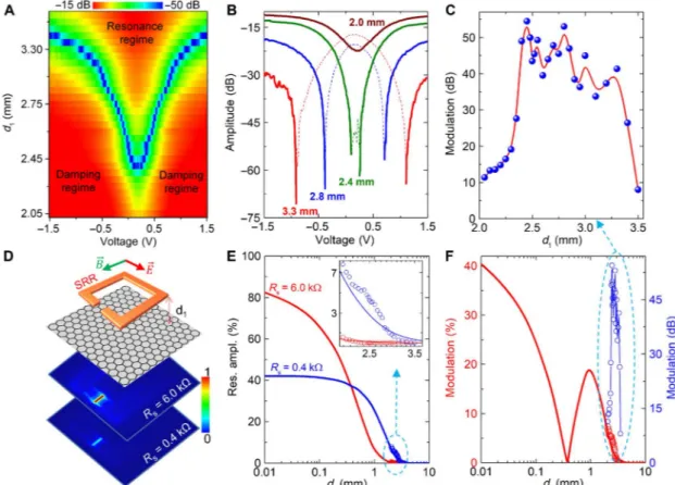
To understand the effect of the separation (d1) between graphene capacitor and metamaterial arrays on the performance of our meta-device, we measured near-field transmission spectrum in the forward
direction at various d1values while sweeping the bias voltage between
±1.5 V. Figure 2A shows the resonance amplitude as a function of d1 and applied bias voltage. We separate the color plot in two regimes: resonance and damping regimes. In resonance regime (above the blue regions), the SRR is not resonating in the forward direction; therefore,
the amplitude increases as d1goes above dc= 2.4 mm. The SRR is
re-sonating in the resonance regime, but the extinction pattern is not at the
Fig. 2. Investigating coupling distance dependence (d1) of the metadevice performance. (A) Variation of the resonance amplitude (Res. ampl.) with d1and bias voltage in the forward direction. Although the bias voltage damps the resonance at the damping regimes, it changes the radiation pattern of SRRs without changing its amplitude in the resonance regimes. (B) Resonance amplitude as a function of bias voltage at various d1, extracted from (A). The solid lines represent damping and dash lines represent resonance regimes. (C) Modulation of transmission amplitude at resonance with bias voltage as a function of d1. Modulation is maximum at dc= 2.4 mm. (D) Schematic drawing for the metadevice structure used in finite element simulation together with simulated electric field distribution on SRR at 6- and 0.4-kilohm sheet resistance (Rs) of single-layer graphene at d1= 2 mm. (E) Simulated variation of resonance amplitude of SRR arrays with d1for Rs= 6 and 0.4 kilohm. The inset shows calculated resonance amplitude variation with experimentally measured ones. (F) Simulated and measured resonance amplitude modulation as a function of d1. The blue scattered circles are experimentally measured amplitude modulation in decibel scale.
on February 25, 2019
http://advances.sciencemag.org/
position of the monopole antenna. It should be emphasized here that the variation in the near-field extinction pattern of SRRs is presented in more detail in Fig. 3. First, the extinction pattern of the SRR is collected toward the antenna position at a critical bias voltage (Vc), and sub-sequently, the damping starts beyond that voltage in the damping
regimes. The blue regions in Fig. 2A show that d1and Vccondition
together to achieve a resonance having an amplitude below−50 dB in
the forward direction at the position of the monopole antenna. In the damping regimes (below the blue region in Fig. 2A), the SRR is always resonating in the forward direction; hence, applied bias voltage damps its resonance. Figure 2B shows line plots of the variation in the
resonance amplitude with the applied bias voltage for some d1values,
extracted from Fig. 2A. Here, the straight lines represent the damping regime, and the dash lines represent the resonance regime. Resonance
amplitude below−50 dB can be achieved for d1≥ dc, and the resonance
can be damped with the bias voltages above Vc(varies for each d1≥ dc).
To find the modulation of the resonance amplitude with the bias voltage,
we compare the resonance amplitude at ±1.5 V and Vcfor each d1values.
We have achieved the maximum modulation of 55 dB at dc= 2.4 mm
(Fig. 2C). The modulation increases very fast for d1< dcand decreases
slowly for d1> dc. More detailed measurements and analysis for the
experimental characterization of the coupling distance (d1) are presented
in section S2. To further investigate the effect of d1on the performance
of our metadevice, we simulate our device in a finite element sim-ulation platform (COMSOL) using the device structure shown in Fig. 2D. We used a single-layer graphene and an SRR coupled to that
graphene at d1in the unit cell. The color plots in Fig. 2D show the
nor-malized electric field intensities on the SRR for 6.0 and 0.4 kilohm sheet resistances (Rs) of the single-layer graphene. The field is confined in the split gap, and doping the single-layer graphene decreases the in-tensity of the electric field. Then, we calculate the resonance
ampli-tude of the SRR as a function of d1for 6.0 and 0.4 kilohm Rsvalues
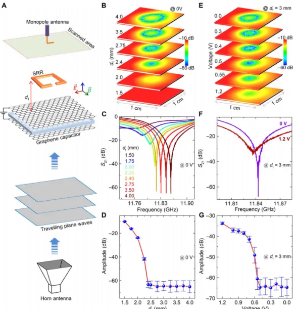
Fig. 3. Near-field characterization of the active metadevices. (A) Near-field scanning technique to map the local scattering parameter (S21) of the device. Scattering parameter provides the magnitude of the local electric field along the direction of the antenna. (B to D) Spatial map, spectrum, and average resonance amplitude of the local scattering parameter of the metadevices probed by a monopole antenna at different graphene-SRR distances at 0 V. (E to G) Voltage dependence of the spatial map, spectrum, and resonance amplitude of the local scattering parameters of device at d1= 3 mm.
on February 25, 2019
http://advances.sciencemag.org/
(Fig. 2E). The amplitudes for both Rsvalues are decreasing with d1 due to the variation in the coupling capacitance. The scattered circles in Fig. 2E and the inset show the measured resonance amplitudes of our metadevice for doped and undoped cases. As a result, there is good agreement between the simulation and the experimental data. Using the calculated resonance amplitudes, we calculate the modulation of the
amplitude in percentage (%) scale as a function of d1(Fig. 3F). The global
maximum is achieved at very short d1values (at 0 mm) and the local
maximum is at d1= 1 mm. Our measured modulation in percent scale
follows the calculated one very well for d1values used in the experiments.
Using the same strategy used for simulation of the metadevices working in the microwave frequencies, we simulated the performance of graphene to control the resonance amplitude of SRRs from terahertz to visible fre-quencies. We have found the critical coupling distances to achieve max-imum modulation in their amplitude both in decibel and percent scales. Detailed results of the simulations performed from microwave to visible frequencies are presented in section S3. As a result of the simulations performed, we conclude that our approach is valid from microwave to visible frequencies in the electromagnetic spectrum.
To explore the tunability of electric field distribution of active metadevices, we used a near-field scanning technique to map the local electric field distributions (47). We placed the device on a computer-controlled motorized stage and recorded the spectrum of local scattering parameter by using a monopole antenna connected to a network an-alyzer (Fig. 3A). First, we examined the critical coupling condition between the graphene electrode and SRR at zero bias voltage. Figure 3B shows the measured local transmission (S21) intensity distribution of metadevices at different graphene-SRR separation. In the near-field of the metadevices, the complete extinction of the microwave signal (that
is, resonance) occurs on a ring-shape region whose radius depends on the graphene-SRR separation. When graphene is very close (<2 mm) to the SRR, the resonance diminishes because of the large dissipation on graphene. Figure 3C shows the transmittance spectrum, and Fig. 3D
shows the average resonance amplitude at different d1values at 0 V.
The resonance depth decreases with an increase in d1and stays nearly
constant for d1values larger than the critical coupling distance (dc) of
2.4 mm. We are limited with the noise level of our measurement sys-tem. Then, we measured the variation of the near-field distribution as
a function of bias voltage at d1= 3 mm (Fig. 3E). Upon increasing the
charge density on graphene electrodes, the extinction ring shrinks fur-ther and diminishes at large voltages. The transmission spectra at 0 and 1.2 V are demonstrated in Fig. 3F. Although the size of the extinc-tion pattern becomes smaller until a critical bias voltage (Vc) of 0.55 V, the resonance amplitude does not change and it is damped beyond that voltage. The critical bias voltage to start damping increases with the
sep-aration distance for d1≥ dc. More details about the imaging near-field
extinction pattern of SRRs are presented in section S4.
DISCUSSION
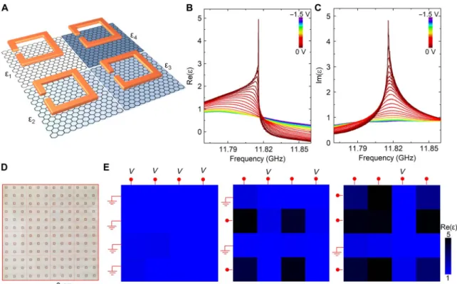
To show the promise of the approach, now we would like to demon-strate the spatial tuning of metamaterials that could open new applica-tions in transformation optics (48). Transformation optics is an emerging field of research aiming to conceal an object by bending or distorting electromagnetic waves using spatially varying metamaterials (49, 50). The ability to control the spatial variation of permittivity and permeability by electrical means would yield new perspectives on adaptive electro-magnetic cloaking and camouflage. By integrating arrays of individually
Fig. 4. Electrically reconfigurable, spatially varying digital metamaterials. (A) Schematic drawing of a digital metamaterial with individually addressable pixels. Controlling the charge density on individual pixels allows us to reconfigure the local dielectric constant. (B and C) The spectra of the calculated real and imaginary part of the effective dielectric constant of a single pixel under different bias voltages. (D and E) The spatial map of the real part of the effective dielectric constant of the device at the resonance condition for different voltage configurations. The effective dielectric constant of the pixels is controlled by passive matrix addressing.
on February 25, 2019
http://advances.sciencemag.org/
addressable metadevices, our approach can be used for voltage-controlled adaptive transformation optics. Figure 4 shows the schematic of the multipixel device. By controlling the local charge density on a pixelated surface by passive matrix addressing, we demonstrate an electrically reconfigurable, spatially varying metadevices. We fabricated a large-area metadevice with 4 × 4 arrays of active pixels. Each pixel contains nine SRRs (3 × 3). We measured the scattering parameter at the center of the pixels and then calculated the local dielectric function. To calculate the dielectric function, we first write the S parameters in terms of imped-ance and refractive index of the metasurface and calculated their roots in terms of S parameters, as given by Chen et al. (51). To overcome the branching problem for the real part of the refractive index, we used Kramers-Kronig relations, as developed by Szabo et al. (52). We used our unit cell size of 11 mm for the effective thickness of our meta-material structure. Figure 4 (B and C) shows the calculated real and imaginary part of the effective dielectric constant. By accumulating charges on a pixel, the local dielectric constant varies from 5 down to 0.8. Figure 4 (D and E) shows spatial maps of the real part of the di-electric constant of the pixelated device at different voltage configura-tions. Details for the spatially varying metadevices are explained in section S5. We were able to reconfigure the spatial variation of the dielectric constant over the device by precisely varying the voltage applied to the rows and columns. It is necessary to point out here that the cross-coupling between the pixels is due to the passive matrix addressing. The fabricated devices are on thin flexible
sub-strates, and therefore, they can be wrapped around nonplanar objects for cloaking applications.
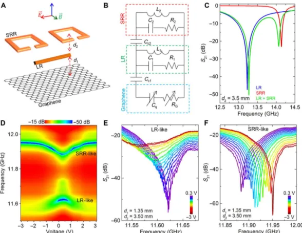
Tuning resonance frequency of a metasurface without modifying its amplitude is one of the challenges for active metadevices. To overcome this challenge, we have implemented a unique metadevice concept to actively control the resonance frequency of the device by electrical means. The metadevice consists of three coupled layers: the first is SRR, second is line resonator (LR) arrays, and third is the graphene capacitor. We used large-area graphene capacitor as an electrically tunable active com-ponent of the metadevice. The unit cell of the metadevice is schemati-cally illustrated in Fig. 5A, where two SRRs are coupled to a single LR at
d2and both of them are coupled to a graphene capacitor at d1below the
LR. Note that each layer is coupled capacitively to each other, and the coupling capacitance is proportional to the distance between them. Small-signal circuit model of the entire metadevice with electrostatic-coupling capacitances are shown in Fig. 5B. Graphene is represented with a tunable quantum capacitance (Cq) and sheet resistance (Rs). Un-coupled single layer of SRR and LR surfaces have their own resonance deeps in transmission spectrum; simulated results are shown in Fig. 5C.
Coupling these layers at d2= 3.5 mm results in two resonance deeps,
where one resonance is SRR-like and the other resonance is LR-like. LR-like resonance is at higher frequencies, and SRR-like resonance is at lower frequencies than the uncoupled states. Our aim here is to actively tune the SRR-like resonance frequency, without changing its amplitude, by selectively damping the LR-like resonance. Therefore, we placed the
Fig. 5. Frequency-tunable active metadevices. (A) Schematic drawing of the designed three-layer frequency-tunable metadevice structure. In a unit cell, two SRRs are coupled to a LR at d2, and a graphene capacitor is coupled to both of them at d1below the LR layer. (B) Small-signal circuit model to represent the three-layer metadevice. (C) Transmission spectrum showing the resonances of coupled (d2= 3.5 mm) and uncoupled SRR and LR metasurfaces. (D) Experimentally measured variation in the transmission spectrum of the three-layer metadevice by means of bias voltages applied to graphene capacitor at d1= 1.35 mm and d2= 3.50 mm. (E) Transmission spectrum showing the resonance damping of LR-like resonance with bias voltage. (F) Transmission spectrum showing the shift in the frequency of the SRR-like resonance with bias voltages without varying its amplitude.
on February 25, 2019
http://advances.sciencemag.org/
graphene capacitor closer to the LR layer than the SRR layer. Transmission spectra measured from the three-layer metadevice as a function of bias
voltages are shown in Fig. 5D for d1= 1.35 mm and d2= 3.50 mm. The
regions with blue color show the resonance amplitude below−50 dB.
Charging graphene capacitor with bias voltages damps the resonance amplitude of the LR-like resonance (Fig. 5E) while shifting the resonance frequency of the like resonance (Fig. 5F). The amplitude of the SRR-like resonance fluctuates with applied bias voltages, but its overall amplitude
stays below−50 dB level. We have obtained a similar active
frequency-tunable metadevice by coupling two uniform SRR layers (see section S6).
CONCLUSION
The results presented here confirm a promising approach for electrically controlled active metadevices. The core idea of the approach is based on the electrical tuning of effective strength of a resonator placed close to a tunable Drude metal. Electrostatic tuning of the charge density on graphene yields broadband controllability on the response of various types of metamaterials both in near- and far-field (sections S7 and S8). These active metadevices enable efficient control of both amplitude (>50 dB) and phase (>90°) of electromagnetic waves. To show the promising uses of the approach, we demonstrated electrically reconfig-urable spatially varying metamaterials and frequency-tunable active metadevices. The operation frequency of these metadevices can be easily scaled up to the terahertz and higher frequencies. Large modulation depth, simple device architecture, and mechanical flexibility are the key attributes of the graphene-enabled active metadevices. We antici-pate that the presented approach could lead to new applications ranging from electrically switchable cloaking devices to adaptive camouflage systems in microwave and terahertz frequencies.
MATERIALS AND METHODS
Fabrication of graphene capacitors
We synthesized large-area (7 × 14 cm2) graphene using a CVD system
on ultrasmooth copper foils (Mitsui Mining and Smelting Company,
Ltd, B1-SBS) under 100 sccm H2and 10 sccm CH4flow for 1 min at
1035°C. After the growth, we transferred the graphene on a flexible 75-mm-thick PVC substrate using hot lamination technique. After etching the Cu in 5 mM aqueous solution of FeCl3, we used two layers of graphene on PVC to fabricate a large-area graphene supercapacitor.
A paper tissue with a thickness of 100mm was used as a spacer between
two graphene electrodes. We first put the tissue on top of one graphene electrode and then ionic liquid (1-butyl-3-methylimidazolium hexa-fluorophosphate). We placed the top graphene electrode and let the ionic liquid disperse between the two graphene electrodes.
Fabrication of metamaterials
To fabricate metamaterial structures, we laminated a 75-mm-thick PVC
laminating film on 10-mm-thick copper foils. We printed the
meta-material structure on the copper foils using Hewlett-Packard Color LaserJet printer (CP2020). We etched the copper in a nitric acid solution. The printed toner functions as an etch mask on copper. With this
tech-nique, we can define metadevices having a feature size as small as 80mm.
Microwave measurements
We used a Keysight E5063A network analyzer for the microwave char-acterization of our device. For near-field measurements, we connected a horn antenna to one channel and a 1.5-cm-long monopole antenna to
the other channel of the network analyzer to measure the S parameters ranging from 7 to 15 GHz. The active metadevice was placed at a specific distance above the monopole antenna, and the horn antenna was used to propagate microwaves in free space. The device is placed on a computer-controlled motorized stage with 1-mm spatial resolution. Both the amplitudes and phases of the received signals were recorded for each location. The monopole antenna was aligned along the electric field of the horn antenna. We connected the Keithley 2400 source mea-sure unit to apply voltage bias. We tuned the voltage manually and re-corded the scattering parameters. For far-field measurements, we used a horn antenna instead of a monopole antenna and placed our devices between two horn antennas to measure far-field S parameters.
SUPPLEMENTARY MATERIALS
Supplementary material for this article is available at http://advances.sciencemag.org/cgi/ content/full/4/1/eaao1749/DC1
section S1. Fabrication and characterization of graphene supercapacitors section S2. Microwave performance of active metadevices in near-field section S3. Electromagnetic modeling and simulation of active metadevices section S4. Imaging near-field extinction pattern of a square SRR section S5. Electrically reconfigurable, spatially varying digital metamaterials section S6. Frequency-tunable active metadevices
section S7. Performance of active metadevices in far field
section S8. Microwave performance of various metadevices in near-field fig. S1. Image of growth, transfer, and etching processes.
fig. S2. Characterization of single-layer graphene.
fig. S3. Large-area graphene supercapacitor and its characterization. fig. S4. Fabrication of large-area SRR structures.
fig. S5. Near-field microwave measurement setup. fig. S6. Modulation of resonance amplitude in percent scale. fig. S7. Modulation of resonance amplitude in decibel scale. fig. S8. Detailed analysis for electrical switching of square SRRs. fig. S9. Time response of the metadevices.
fig. S10. Conductivity of graphene.
fig. S11. Simulating performance of metadevices working in microwave.
fig. S12. Simulated transmission spectrum of active metadevices working in microwave. fig. S13. Dependence of the resonance amplitude modulation to the period of SRRs in arrays of them in microwave.
fig. S14. Simulating performance of metadevices working in terahertz. fig. S15. Simulating performance of metadevices working in far IR. fig. S16. Simulating performance of metadevices working in mid IR. fig. S17. Simulating performance of metadevices working in near IR. fig. S18. Simulating performance of metadevices working in visible.
fig. S19. Simulating performance of metadevices in near IR using Au metal with its frequency-dependent n-k constants.
fig. S20. Simulating performance of metadevices in visible using Au metal with its frequency-dependent n-k constants.
fig. S21. Dependence of optimum coupling distance to resonance wavelength ratio (dopt1 :=lr)
onlr.
fig. S22. Device structure and experimental setup used for imaging near-field extinction pattern of SRRs.
fig. S23. Variation of extinction pattern with coupling distance d1at 0 V.
fig. S24. Variation of extinction pattern with bias voltage at d1= 3 mm.
fig. S25. Variation of extinction pattern with bias voltage at d1= 3.5 mm.
fig. S26. Device structure of large-area, pixelated, reconfigurable metadevices. fig. S27. Transmission (S21) patterns of pixelated, reconfigurable metadevices obtained by
passive matrix addressing.
fig. S28. Real part of patterned dielectric constant on a large-area metadevice. fig. S29. Imaginary part of patterned dielectric constant on a large-area metadevice. fig. S30. Voltage response of transmission (S21) and retrieved dielectric constants in pixelated
metadevices.
fig. S31. SRR arrays coupled to LR arrays.
fig. S32. Finding optimum d1to achieve maximum shift in resonance frequency of SRRs at
d2= 3.5 mm.
fig. S33. Transmission spectrums showing the shift in resonance frequency of SRR arrays while damping the resonance amplitude of LRs.
fig. S34. Coupling two identical SRR arrays.
on February 25, 2019
http://advances.sciencemag.org/
fig. S35. Tuning resonance frequency of SRR arrays coupled to its twin. fig. S36. Active tuning of magnetic resonance.
fig. S37. Active tuning of electric resonance excited by a horizontally traveling electromagnetic waves on SRR arrays by graphene supercapacitor.
fig. S38. Electrically switchable metadevices made of a dense SRR arrays measured in far field. fig. S39. Switching transmission amplitude and phase of various type metamaterials coupled to graphene supercapacitors by sweeping bias voltage from 0 to−1.5 V in near-field. fig. S40. Switching transmission amplitude and phase of various type metamaterials coupled to graphene supercapacitors by sweeping bias voltage from 0 to−1.5 V measured in near-field.
fig. S41. Schematic drawings of metamaterials fabricated throughout this work with their dimensions.
REFERENCES AND NOTES
1. H. Tao, W. J. Padilla, X. Zhang, R. D. Averitt, Recent progress in electromagnetic metamaterial devices for terahertz applications. IEEE J. Sel. Top. Quantum Electron. 17, 92–101 (2011).
2. J. B. Pendry, D. Schurig, D. R. Smith, Controlling electromagnetic fields. Science 312, 1780–1782 (2006).
3. E. Ozbay, Plasmonics: Merging photonics and electronics at nanoscale dimensions. Science 311, 189–193 (2006).
4. D. Shin, Y. Urzhumov, Y. Jung, G. Kang, S. Baek, M. Choi, H. Park, K. Kim, D. R. Smith, Broadband electromagnetic cloaking with smart metamaterials. Nat. Commun. 3, 1213 (2012).
5. N. I. Zheludev, Y. S. Kivshar, From metamaterials to metadevices. Nat. Mater. 11, 917–924 (2012).
6. Y. Urzhumov, J. Seung Lee, T. Tyler, S. Dhar, V. Nguyen, N. M. Jokerst, P. Schmalenberg, D. R. Smith, Electronically reconfigurable metal-on-silicon metamaterial. Phys. Rev. B 86, 075112 (2012).
7. M. D. Goldflam, T. Driscoll, B. Chapler, O. Khatib, N. Marie Jokerst, S. Palit, D. R. Smith, B.-J. Kim, G. Seo, H.-T. Kim, M. Di Ventra, D. N. Basov, Reconfigurable gradient index using VO2memory metamaterials. Appl. Phys. Lett. 99, 044103 (2011).
8. J. P. Turpin, J. A. Bossard, K. L. Morgan, D. H. Werner, P. L. Werner, Reconfigurable and tunable metamaterials: A review of the theory and applications. Int. J. Antennas Propag. 2014, 429837 (2014).
9. T. H. Hand, S. A. Cummer, Reconfigurable reflectarray using addressable metamaterials. IEEE Antennas Wirel. Propag. Lett. 9, 70–74 (2010).
10. F. Costa, A. Monorchio, G. P. Vastante, Tunable high-impedance surface with a reduced number of varactors. Ieee Antennas Wirel. Propag. Lett. 10, 11–13 (2011).
11. O. Reynet, O. Acher, Voltage controlled metamaterial. Appl. Phys. Lett. 84, 1198 (2004).
12. K. Aydin, E. Ozbay, Capacitor-loaded split ring resonators as tunable metamaterial components. J. Appl. Phys. 101, 024911 (2007).
13. D. H. Werner, D.-H. Kwon, I.-C. Khoo, Liquid crystal clad near-infrared metamaterials with tunable negative-zero-positive refractive indices. Opt. Express 15, 3342–3347 (2007).
14. D. F. Gardner, J. S. Evans, I. I. Smalyukh, Towards reconfigurable optical metamaterials: Colloidal nanoparticle self-assembly and self-alignment in liquid crystals. Mol. Cryst. Liq. Cryst. 545, 1227–1245 (2011).
15. A. B. Golovin, O. D. Lavrentovich, Electrically reconfigurable optical metamaterial based on colloidal dispersion of metal nanorods in dielectric fluid. Appl. Phys. Lett. 95, 254104 (2009).
16. J. Han, A. Lakhtakia, Semiconductor split-ring resonators for thermally tunable terahertz metamaterials. J. Mod. Opt. 56, 554–557 (2009).
17. J. G. Han, A. Lakhtakia, C.-W. Qiu, Terahertz metamaterials with semiconductor split-ring resonators for magnetostatic tunability. Opt. Express 16, 14390–14396 (2008). 18. J. Wang, S. Liu, S. Guruswamy, A. Nahata, Reconfigurable liquid metal based terahertz
metamaterials via selective erasure and refilling to the unit cell level. Appl. Phys. Lett. 103, 221116 (2013).
19. H.-T. Chen, W. J. Padilla, J. M. O. Zide, A. C. Gossard, A. J. Taylor, R. D. Averitt, Active terahertz metamaterial devices. Nature 444, 597–600 (2006).
20. H.-T. Chen, W. J. Padilla, M. J. Cich, A. K. Azad, R. D. Averitt, A. J. Taylor, A metamaterial solid-state terahertz phase modulator. Nat. Photonics 3, 148–151 (2009).
21. M. J. Dicken, K. Aydin, I. M. Pryce, L. A. Sweatlock, E. M. Boyd, S. Walavalkar, J. Ma, H. A. Atwater , Frequency tunable near-infrared metamaterials based on VO2phase
transition. Opt. Express 17, 18330–18339 (2009).
22. T. Driscoll, S. Palit, M. M. Qazilbash, M. Brehm, F. Keilmann, B.-G. Chae, S.-J. Yun, H.-T. Kim, S. Y. Cho, N. Marie Jokerst, D. R. Smith, D. N. Basov, Dynamic tuning of an infrared hybrid-metamaterial resonance using vanadium dioxide. Appl. Phys. Lett. 93, 024101 (2008).
23. J.-Y. Ou, E. Plum, J. Zhang, N. I. Zheludev, An electromechanically reconfigurable plasmonic metamaterial operating in the near-infrared. Nat. Nanotechnol. 8, 252–255 (2013).
24. H. Tao, A. C. Strikwerda, K. Fan, W. J. Padilla, X. Zhang, R. D. Averitt, MEMS based structurally tunable metamaterials at terahertz frequencies. J. Infrared Millim. Terahertz Waves 32, 580–595 (2011).
25. H. Tao, A. C. Strikwerda, K. Fan, W. J. Padilla, X. Zhang, R. D. Averitt, Reconfigurable terahertz metamaterials. Phys. Rev. Lett. 103, 147401 (2009).
26. F. S. Ma, Y.-S. Lin, X. Zhang, C. Lee, Tunable multiband terahertz metamaterials using a reconfigurable electric split-ring resonator array. Light Sci. Appl. 3, e171 (2014).
27. I. M. Pryce, K. Aydin, Y. A. Kelaita, R. M. Briggs, H. A. Atwater, Highly strained compliant optical metamaterials with large frequency tunability. Nano Lett. 10, 4222 (2010).
28. B. Sensale-Rodriguez, R. Yan, M. M. Kelly, T. Fang, K. Tahy, W. S. Hwang, D. Jena, L. Liu, H. G. Xing, Broadband graphene terahertz modulators enabled by intraband transitions. Nat. Commun. 3, 780 (2012).
29. B. Sensale-Rodriguez, T. Fang, R. Yan, M. M. Kelly, D. Jena, L. Liu, H. G. Xing, Unique prospects for graphene-based terahertz modulators. Appl. Phys. Lett. 99, 113104 (2011).
30. L. Ju, B. Geng, J. Horng, C. Girit, M. Martin, Z. Hao, H. A. Bechtel, X. Liang, A. Zettl, Y. R. Shen, F. Wang, Graphene plasmonics for tunable terahertz metamaterials. Nat. Nanotechnol. 6, 630–634 (2011).
31. B. Sensale-Rodriguez, R. Yan, L. Liu, D. Jena, H. G. Xing, Graphene for reconfigurable terahertz optoelectronics. Proc. IEEE 101, 1705–1716 (2013).
32. P. Tassin, T. Koschny, C. M. Soukoulis, Graphene for terahertz applications. Science 341, 620–621 (2013).
33. K. F. Mak, L. Ju, F. Wang, T. F. Heinz, Optical spectroscopy of graphene: From the far infrared to the ultraviolet. Solid State Commun. 152, 1341–1349 (2012).
34. N. Rouhi, S. Capdevila, D. Jain, K. Zand, Y. Y. Wang, E. Brown, L. Jofre, P. Burke, Terahertz graphene optics. Nano Res. 5, 667–678 (2012).
35. P. Q. Liu, I. J. Luxmoore, S. A. Mikhailov, N. A. Savostianova, F. Valmorra, J. Faist, G. R. Nash, Highly tunable hybrid metamaterials employing split-ring resonators strongly coupled to graphene surface plasmons. Nat. Commun. 6, 8969 (2015).
36. S. H. Lee, M. Choi, T.-T. Kim, S. Lee, M. Liu, X. Yin, H. K. Choi, S. S. Lee, C.-G. Choi, S.-Y. Choi, X. Zhang, B. Min, Switching terahertz waves with gate-controlled active graphene metamaterials. Nat. Mater. 11, 936–941 (2012).
37. N. K. Emani, T.-F. Chung, X. Ni, A. V. Kildishev, Y. P. Chen, A. Boltasseva, Electrically tunable damping of plasmonic resonances with graphene. Nano Lett. 12, 5202–5206 (2012). 38. Y. Yao, M. A. Kats, P. Genevet, N. Yu, Y. Song, J. Kong, F. Capasso, Broad electrical tuning of
graphene-loaded plasmonic antennas. Nano Lett. 13, 1257–1264 (2013).
39. J. Kim, H. Son, D. J. Cho, B. Geng, W. Regan, S. Shi, K. Kim, A. Zettl, Y.-R. Shen, F. Wang, Electrical control of optical plasmon resonance with graphene. Nano Lett. 12, 5598–5602 (2012).
40. S. H. Lee, J. Choi, H.-D. Kim, H. Choi, B. Min, Ultrafast refractive index control of a terahertz graphene metamaterial. Sci. Rep. 3, 2135 (2013).
41. E. O. Polat, C. Kocabas, Broadband optical modulators based on graphene supercapacitors. Nano Lett. 13, 5851–5857 (2013).
42. I. Baylam, M. N. Cizmeciyan, S. Ozharar, E. O. Polat, C. Kocabas, A. Sennaroglu, Femtosecond pulse generation with voltage-controlled graphene saturable absorber. Opt. Lett. 39, 5180–5183 (2014).
43. E. O. Polat, O. Balci, C. Kocabas, Graphene based flexible electrochromic devices. Sci. Rep. 4, 6484 (2014).
44. O. Balci, E. O. Polat, N. Kakenov, C. Kocabas, Graphene-enabled electrically switchable radar-absorbing surfaces. Nat. Commun. 6, 6628 (2015).
45. J. Xia, F. Chen, J. Li, N. Tao, Measurement of the quantum capacitance of graphene. Nat. Nanotechnol. 4, 505–509 (2009).
46. S. Bae, H. Kim, Y. Lee, X. Xu, J.-S. Park, Y. Zheng, J. Balakrishnan, T. Lei, H. R. Kim, Y. I. Song, Y.-J. Kim, K. S. Kim, B. Özyilmaz, J.-H. Ahn, B. H. Hong, S. Iijima, Roll-to-roll production of 30-inch graphene films for transparent electrodes. Nat. Nanotechnol. 5, 574–578 (2010).
47. S. Sun, Q. He, S. Xiao, Q. Xu, X. Li, L. Zhou, Gradient-index meta-surfaces as a bridge linking propagating waves and surface waves. Nat. Mater. 11, 426–431 (2012). 48. H. Chen, C. T. Chan, P. Sheng, Transformation optics and metamaterials. Nat. Mater. 9,
387–396 (2010).
49. T. J. Cui, M. Q. Qi, X. Wan, J. Zhao, Q. Cheng, Coding metamaterials, digital metamaterials and programmable metamaterials. Light Sci. Appl. 3, e218 (2014).
50. C. Della Giovampaola, N. Engheta, Digital metamaterials. Nat. Mater. 13, 1115–1121 (2014).
51. X. Chen, T. M. Grzegorczyk, B.-I. Wu, J. Pacheco Jr., J. A. Kong, Robust method to retrieve the constitutive effective parameters of metamaterials. Phys. Rev. E 70, 016608 (2004).
on February 25, 2019
http://advances.sciencemag.org/
52. Z. Szabo, G.-H. Park, R. Hedge, E.-P. Li, A unique extraction of metamaterial parameters based on Kramers–Kronig relationship. IEEE Trans. Microw. Theory Tech. 58, 2646–2653 (2010).
Acknowledgments
Funding: This work was supported by the European Research Council (ERC) Consolidator (grant no. ERC-682723 SmartGraphene) and by the Scientific and Technological Research Council of Turkey (TUBITAK) (grant no. 114F052). O.B. and N.K. acknowledge the fellowship provided by TUBITAK-BIDEB 2211 and 2215. Author contributions: O.B. and C.K. conceived the idea and planned the experiments, analyzed the data, and wrote the manuscript. O.B. fabricated the samples, performed the experiments, and made the simulations. N.K., S.B., and E.O.P. helped for the synthesis of graphene, fabrication of the devices, and microwave measurements. E.K., S.C., H.C., and E.Ö. helped for the simulations and interpretations of the experimental results. All authors discussed the results and contributed to the scientific
interpretation, as well as to the writing of the manuscript. Competing interests: The authors declare that they have no competing interests. Data and materials availability: All data needed to evaluate the conclusions in the paper are present in the paper and/or the Supplementary Materials. Additional data related to this paper may be requested from the authors.
Submitted 23 June 2017 Accepted 30 November 2017 Published 5 January 2018 10.1126/sciadv.aao1749
Citation:O. Balci, N. Kakenov, E. Karademir, S. Balci, S. Cakmakyapan, E. O. Polat, H. Caglayan, E. Özbay, C. Kocabas, Electrically switchable metadevices via graphene. Sci. Adv. 4, eaao1749 (2018).
on February 25, 2019
http://advances.sciencemag.org/
Ekmel Özbay and Coskun Kocabas
Osman Balci, Nurbek Kakenov, Ertugrul Karademir, Sinan Balci, Semih Cakmakyapan, Emre O. Polat, Humeyra Caglayan,
DOI: 10.1126/sciadv.aao1749 (1), eaao1749.
4 Sci Adv
ARTICLE TOOLS http://advances.sciencemag.org/content/4/1/eaao1749
MATERIALS
SUPPLEMENTARY http://advances.sciencemag.org/content/suppl/2017/12/22/4.1.eaao1749.DC1
REFERENCES
http://advances.sciencemag.org/content/4/1/eaao1749#BIBL This article cites 52 articles, 3 of which you can access for free
PERMISSIONS http://www.sciencemag.org/help/reprints-and-permissions
Terms of Service Use of this article is subject to the
registered trademark of AAAS.
is a
Science Advances
Association for the Advancement of Science. No claim to original U.S. Government Works. The title
York Avenue NW, Washington, DC 20005. 2017 © The Authors, some rights reserved; exclusive licensee American (ISSN 2375-2548) is published by the American Association for the Advancement of Science, 1200 New
Science Advances
on February 25, 2019
http://advances.sciencemag.org/