2 (2), 2008, 293-314
©BEYKENT UNIVERSITY
SLOT-LOADED MICROSTRIP ANTENNA
DESIGN OF TRANSCEIVER FOR WIRELESS
DATA COMMUNICATION IN ISM BAND
Suna Beyza ARDIÇ
1, Adnan KAYA
2, Özlem COŞKUN
3Department of Electronics and Communication
Engineering Süleyman Demirel University, Isparta, Turkey, 32260
[email protected] [email protected] [email protected]
Received: 12 June 2008, Accepted: 26 June 2008
ABSTRACT
This paper is a presentation of the designed procedure of the microstrip antenna operating at 2.4 GHz transceiver for RF front-end for ISM band digital wireless communication. The aim of this project is to present several types of compact microstrip patch antennas for ISM 2.4 GHz band, and then to compare and interpret the results. Besides, some information was provided as to the ISM band and transceiver systems. The different geometries of microstrip antennas are simulated such as recessed microstrip line feed, microstrip patch arrays, slot-loaded microstrip patch arrays, dual-band and slot-loaded rectangular microstrip patch with AWR Microwave Office Software, using Moment Method. A slot-loaded rectangular microstrip antenna with meandering slots in the ground plane was designed; then this antenna was simulated and studied in detail.
Furthermore, the effect of the results is studied by changing the parameters of the meandered antenna. The results also show that the return loss levels of the meandered antennas vary from -12.8 dB to -18.9 dB. The designed antenna operates at 2.4 GHz with 105 MHz bandwidth, having 1 of -12.8 dB at resonant frequency.
Key words: 2.4 GHz transceiver, ISM band, microstrip antenna.
ÖZET
Bu makalede 2.4 GHz ISM bandı sayısal kablosuz haberleşme sistemlerinde kullanılabilecek RF alıcı-verici sistemler için tasarlanan mikroşerit anten çeşitleri ve tasarımları gösterilmiştir. Bu çalışmadaki amaç, 2.4 GHz frekansında çalışan, çeşitli kompakt mikroşerit anten yapılarını göstermek ve
anten parametrelerinin sonuçlar üzerindeki etkisini incelemektir. Ayrıca ISM bandı alıcı-verici sistemleri ve bu sistemlerle uyumlu olacak anten geometrileri karşılaştırılmıştır.
Mikroşerit hat besleme, mikroşerit yama dizileri, yarık yüklü yama anten, yarık yüklü yama anten dizileri ve çift bant antenler Moment Metodunu kullanan AWR Microwave Office programı ile tasarlanmıştır. Yarık yüklü yama ve toprak düzleminde yarık açılan tasarlanan anten detaylı çalışıldı ve antenin parametre değişikliklerinin sonuçlar üzerindeki etkisi incelenmiştir. Antenlerin geri dönüş kaybının -12.8 dB ile -18.9 dB arasında değiştiği gösterilmiştir. Tasarlanan anten 2.4 GHz de, 105 MHz band genişliği ile -12.8 dB geri dönüş kaybına sahiptir.
Anahtar kelimeler: Mikroşerit antenler, ISM band, alıcı-verici sistemler
INTRODUCTION
In the market of wireless local area network (WLAN), multi-standard transceivers have been the trend. The IEEE 802.11b standard at the 2.4 GHz ISM band provides data rates up to 11 Mbitds [1], and the 802.11a standard at the 5GHz U-NI1 bands provides data rates up to 54 Mbitds using OFDM modulation [2]. Released in 2003, the 802.11g standard, operated at the same band of 802.11b [3]. Many products in the market can support each of the standards simultaneously, and the employed transceiver architectures are usually the direct-conversion ones. For low-cost CMOS integration, direct conversion to dc or low IF is common, but problems such as dc offset, I/Q mismatch, self-mixing, power amplifier pull, flicker noise, etc., have been compromised to achieve acceptable system performance.
CMOS RF system performance heavily depends on architecture and actual implementation. A dual-mode CMOS RF transceiver solution is presented, which implements all transmit and receive functions for both Bluetooth and 802.11b in a single chip without doubling the required silicon area to further reduce the combined system cost [4,5].
Direct up/down conversion is known to exhibit many technical difficulties although it greatly simplifies the system. In the transmitter, high-power transmitter output can pull the sensitive VCO frequency and degrade system performance. A common remedy for this is to use a frequency doublers or divider to avoid using the same frequency VCO. This work uses a VCO running at 2/3 of the carrier frequency so that the I/Q signal generation may be
simplified using a divide-by-2 circuit. The 2/3 of the carrier frequency is generated using a fractional-N frequency synthesizer with an on-chip loop filter. Rather than using the direct modulation on the carrier, the frequency translation from dc to RF is done in double conversion. Also, the receiver path uses the same double conversion. Bluetooth uses a low-IF system, while WLAN uses a dc system [7,9]. The reason to avoid the direct conversion to dc
in Bluetooth is that in FSK, the frequency offset between the transmitter and the receiver shows up also as a dc offset. Although sophisticated offset cancellation and/or digital processing may overcome some of the difficulties, the direct-conversion receiver is slow for frequency-hopping applications due to the long time constant associated with low-pass filtering and dc offset cancellation.
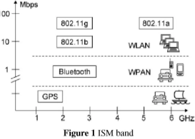
In the 2.4GHz ISM band, three prominent RF data link standards, Bluetooth and 802.11b/g, coexist as shown in Figure 1 [6].
1 2 3 ^ 5
Figure 1 ISM band
They differ distinctly from one another, and demand different level of RF specifications. Bluetooth is a frequency-hopping spread-spectrum system with GFSK modulation in the 2.4GHz ISM band using a low modulation index of about 0.3. 802.11b WLAN is a direct sequence spread-spectrum system with CCK modulation, but 802.11g is a QAM-based OFDM system, which requires high linearity in RF front/rear-ends and the low phase noise synthesizer, although phase noise is partly canceled using pilot channels .
In technical terms, Bluetooth and 802.11b standards can share RF front/rear-ends and the frequency synthesizer [12,13]. The dual-mode solution in this work maximizes hardware usage to have a compact RF solution for both standards. In order to merge two different transceiver functions into one, two systems need to be closely examined. The difference in system bandwidth can be easily overcome using a programmable channel filter, but the difference in modulation schemes dictates the use of different architectures.
The GFSK signal is a constant envelope signal, which contains data in its instantaneous frequency, while the QPSK signal should be gain-controlled for synchronous detection. For these modulation schemes, the most common approaches for the receivers are band pass low-IF processing for Bluetooth and low-pass zero-IF processing for 802.11b [10,13]. For transmitters, zero-IF to RF processing is often used for both schemes.
A typical wireless modem antenna is realized as a monopole mounted on the top of the transceiver. The omni-directional radiation pattern of such an antenna ensures reliable communication regardless of its orientation, but part of the power emitted is absorbed by the user's body. Human body exposure to electromagnetic radiation at frequencies around and above 900 MHz may be hazardous under certain circumstances. The obtained experimental results confirm that this antenna can be used effectively as a building block for ISM (2.4 GHz) band applications. The antenna has reduced radiation towards the device (wireless modem, access point etc.) ensures reliable communication regardless of the antenna orientation. The antenna can be produced at low cost, with fairly good matching. The design is straightforward to implement in MMIC and MIC and allows for easy insertion of printed antennas for a multitude of applications. As a result of this demand we produce a microstrip antenna which is used in 2.4 GHz ISM band [14].
Potential applications of the microstrip antennas for industrial, scientific and medical (ISM)-band cordless telephones or wireless local area networks (WLAN). These designed microstrip antennas can be used in ISM Band. ISM (Industrial, scientific and medical) band were originally reserved internationally for the use of RF electromagnetic fields for industrial, scientific and medical purposes. IEEE 802.11b and 802.11g protocols also use the 2.4 GHz ISM band.
The microstrip antenna is one of the most preferable for small equipment, especially when a built-in antenna is required. It has many advantages such as low profile and easy fabrication. However for low-frequency applications, the microstrip size becomes too large for practical implementation. One of the problems in microstrip antenna technology is the reduction of the antenna sizes. Indeed, it remains quite difficult to miniaturize such radiating elements because these efforts generally conflict with electrical limitations or cost considerations.
Together with recent developments in communications, the need for compact antennas has greatly increased. Electronic equipment has rapidly reduced in physical size due to the development of integrated circuits, especially in wireless communications; the demand for the smaller antennas is quite strong. However, requirements on antenna performance on such small equipment are becoming increasingly severe, since the antenna performance should not be significantly degraded as the size becomes smaller.
Rapid progress in wireless communication could replace wired communication networks in the near future in which antennas should play a more important role. Microstrip antennas are used in a broad range of applications from communication systems to biomedical systems, primarily due to several attractive properties such as light weight, low profile, low production cost,
conformability, reproducibility, reliability and ease in fabrication and integration with solid state devices.
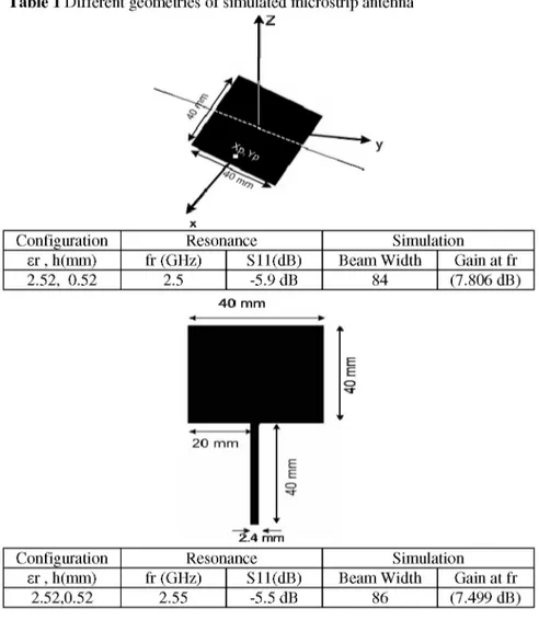
Several techniques for reducing the size of the patch have been presented in the literature such as using a substrate with high dielectric constant, incorporating a shorting pin in a microstrip patch, use of short circuit, cutting slots in radiating patch and by partially filled high permittivity substrate and antenna arrays[8,11,12,15,16]. Some samples of these configurations are designed and simulated as shown in Table 1.
Table 1 Different geometries of simulated microstrip antenna + Z
x
Configuration Resonance Simulation er , h(mm) fr (GHz) S11(dB) Beam Width Gain at fr 2.52, 0.52 2.5 -5.9 dB 84 (7.806 dB) 4 0 m m 40 m m 20 m m 40 m m m m
Configuration Resonance Simulation er , h(mm) fr (GHz) S11(dB) Beam Width Gain at fr
< »
Configuration Resonance Simulation er , h(mm) fr (GHz) S11(dB) Beam Width Gain at fr
2.52,0.52 2.55 -12.8 dB 88 (7.83 dB)
t
• CLi
Configuration Resonance Simulation er , h(mm) fr (GHz) S11(dB) Beam
Width
Gain at fr er , h(mm)
Port1 Port2 Port1 Port2
Beam Width
Gain at fr 2.52, 0.52 2.52 2.15 -9 dB -4 dB -
-Configuration Resonance Simulation er , h(mm) fr (GHz) S11(dB) Beam Width Gain at fr
Configuration Resonance Simulation er , h(mm) fr (GHz) S11(dB) Beam Width Gain at fr
3,0.78 2.5 -6.1 dB 91 (7.646 dB)
Configuration Resonance Simulation er , h(mm) fr (GHz) S11(dB) Beam Width Gain at fr
i
port
Configuration Resonance Simulation er , h(mm) fr (GHz) S11(dB) Beam Width Gain at fr
2.7,0.52 2.5 -10.19 dB 27 (11.03 dB)
Configuration Resonance Simulation er , h(mm) fr (GHz) S11(dB) Beam Width Gain at fr
2.52,0.52 2.1 -8 dB 75 (4.946 dB)
THEORETICAL CONSIDERATIONS
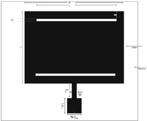
The proposed antenna geometry is shown in Figure 2. The patch is feed by a coaxial probe. The feed position is calculated by using modal expansion cavity model theory, for a 50 Q coaxial cable. The notch has been cut along the patch width in such a way that it must be lie at a symmetrical distance from both edges of the patch.
w u.
Wf5o
Figure 2 Geometry of a the proposed compact broadband meandered
rectangular microstrip antenna
According to cavity-model theory, a microstrip patch antenna can be modeled as a parallel LCR circuit. The current flows from the feeding point to the top and bottom edges of the patch. The electric and magnetic-field discontinuities occur across the notch. The effect of the notch will be both capacitive and inductive.
2.1 EQUIVALENT CIRCUIT MODEL
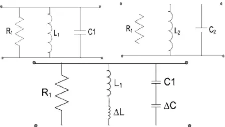
The equivalent circuit corresponding to this current flowing on the patch is shown in Figure 3.
Figure 3 a) Equivalent circuit of the rectangular microstrip patch antenna b)
Corresponding to the current flowing around the notch c) Simplified circuit In this figure, C, L and R are the capacitance, inductance and radiation resistance of the patch, respectively, given by [17]
££ LW
o — c o s -2( ^ 0 )2h
L
(1)Where L is the length of the patch. W is the width of the patch, h is the thickness of the substrate. ee is the effective dielectric constant [17].
£
£ + 1 + £ -
1(i+12h )
- 12 2 W
(2)Where er is the relative dielectric constant of the substrate.
* =
1 WrC1
(3) Where Qr and wr are the quality factor and resonance frequency of the patch,
respectively, given by [17]:
Qr
4 frh
(4)Where c is the velocity of light in free space, and fr is the resonance frequency of the patch.
The input impedance of the resonant circuit is calculated as following:
z
1 patch 1 1 ( 5 )( - +
jwC
+ — ) ( 5 )Ri
jwL
The other current is flowing around the notch on the patch. The equivalent circuit corresponding to this current is shown in Figure 3 (b), where C1, L1 and
R1 have their usual meaning and additional series inductance AL and
capacitance A C due to the notch effect as
AL =
(—)2 (6)8 L
Where ¡1 ° = 4 n X 1 °- 7, l is the equivalent length of the notch and,
AC = (|).C
S(7)
L
Where Cs is the gap capacitance. The input impedance of the resonant circuit
shown in Figure 3(b) can be computed from the simplified circuit shown in Figure 3(c) as follows:
z
1 patch 1 1 /ON.(— + JwC
2+ — )
(8) R J W L2 r CXACC
2 = —1 (9) 2C +AC
WL2 = L +AL
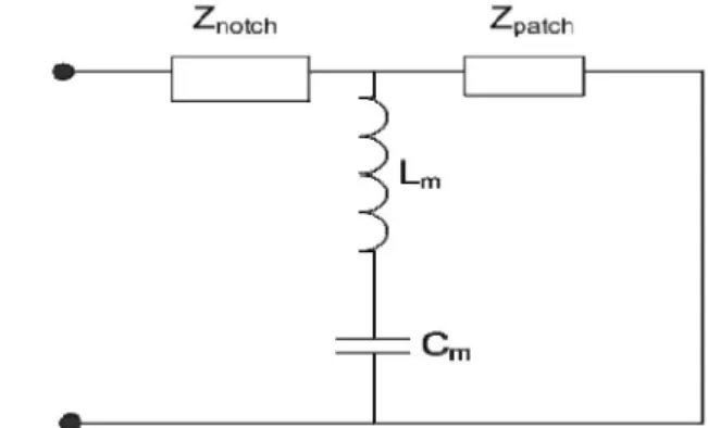
(10)These two resonant circuits are coupled together and form a dual resonant circuit for dual-band as shown in Figure 4. Here, both the inductive and capacitive coupling has been considered.
-paler
Figure 4 Equivalent circuit of the notched microstrip patch antenna
The coupling coefficient between these two resonators is given by;
1
C p
V Q Q
(11) Where Qi is the quality factor of the resonant circuit due to normal current, given by
01
wL
1
(12) and Q2 is quality factor of the resonant circuit due to the notch effect given by
wL
n0 2
R
(13)Then the input impedance of the notched rectangular microstrip patch antenna can be computed from the simplified circuit shown in Figure 4 as follows:
Zin = Znotch + ( ^Zm = j w L m +
Z Z )
patch' m 'Z + Z
patch m j w Cm (14) (15) Using equation (14) the reflection coefficient, can be computed as follows:Z - Z
r • o ins
Z
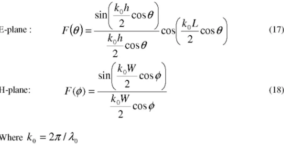
- Z o ins (16)The equations for radiation patterns of E and H planes of the microstrip antenna: E-plane : H-plane:
sin
F (0)
=-sin
( k0
hcos 0
^
,k o h
cos0
2
(kW
cos
knLcos 6
(17)F W =•
2
cos^
kW
,
0cos^
(18)2
Where k 0 = 2 n / 10MICROSTRIP ANTENNA DESIGN AND SIMULATION
First, a reference antenna (RA) i.e., a rectangular microstrip antenna having a size (L, W) = (11.33, 15.2) mm [14] fed by a 50Q center fed microstrip line feed having dimension (Lf5o, Wf5o) = (6.187, 3.1) mm through a quarter wave
transformer of size (Lt, Wt) = (4.922, 0.500) mm was designed for the
operating frequency 6 GHz for TM10 mode [15]. FR4 has a relative
permittivity of 4.4 and a thickness of 1.6mm and it has been used as a substrate material as shown in Table 2. Here the microstrip line feed is used to excite the patch as the planar feed makes the structure suitable for integration with associated microwave circuitry.
Table 2 Specifications of FR4
2
Substrate Material Dielectric Constant £r Loss Tangent tanS Dielectric Thickness h Copper Thickness FR4 Fiberglass 4.5-4.9 0.001 1.6 1^m Later two parallel narrow rectangular slots were etched in the rectangular patch close to the radiating edge with a spacing S = 0.1mm. The length of the slot, Ls, = 14.2mm and slot width Ws, = 1mm. This slot-loaded rectangular patch isin turn meandered using three identical narrow slots embedded in the antenna's ground plane and aligned with an equal spacing of L/4 parallel to the rectangular patch radiating edge as shown in Figure 5 that is 3D geometry of meandered antenna.
These embedded slots are narrow Wg and Lg the slot lengths inside and outside
Figure 5 The 3D geometry of meandered antenna
The patch with W at Meandered-II antenna is fixed to be 14.2 mm where as the slot width Ws was varied from 1 to 0.5 mm and studied in detail. The slot
width Ws at Meandered-III antenna is fixed to be 14.2 mm where as patch
width W was varied from 15.3 to 16.8 mm and studied in detail. The return losses are shown in Figure 6.
1A 1A Frtqufliey (GH:)
Figure 6 Return loss characteristics of the meandered antennas versus
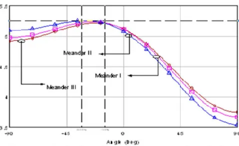
E- Plane radiation patterns can be seen in Figure 7 and Figure 8.
I 1
1 1
r.feandlï II J1 1
Meander 1 f tiantfer III | • ^V
1 1
t 1
~fO -*S O ? ( Al git 'tcg.hFigure 7 Simulated E plane radiation patterns for proposed meandered
antennas
CI dB
•2C-dB
-40 dB
4-Figure 8 E- Plane radiation patterns
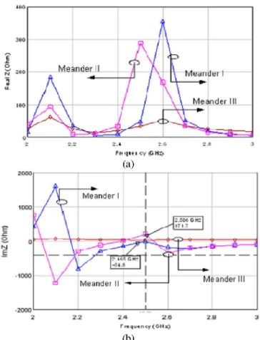
The input impedance characteristics of the meandered antennas are presented in Figure 9.
Figure 9 Input impedance characteristics of the meandered antennas versus
frequency (a) Real impedance (b) Imaginary impedance
The normalized far field radiation in the specified direction for all polarizations and the total power characteristics is shown in Table 3. The total power is defined as the sum of the power contained in E0 and E®:
TPwr
—r w I 9(I E
240n
+
| 2
E< \
)
(19)The principal plane cut captures the total power in all polarizations, and fixes the values of frequency and ® while sweeping 6 from -90 to 90 degrees or -n /2 to n /2 radians. The total power result is normalized to Pave an integration of
the power (in all polarizations) in the upper hemisphere divided by 4n (asterisk denotes complex conjugate values):
, 2 n n / 2 P
ve = T - R e
J J ( E
SB * - E
rH l ) s i n â d â d ^
O
n n n 0 0rPwr (0,0)
n n —<ö<—,è=const 2 2 r (20) (21)Simulated normalized far field radiation in the specified direction and polarization is presented in Table 4.
Table 3 Radiation characteristics of the meandered antennas Antenna The normalized far
Type field radiation for all polarizations (Q=0) Total power (25 dB ) U CÖ Ö s
ü I
J <
u 2 İH S J2 0 c3 C u < £ c w fi c3 53Table 4 Radiation characteristics of the meandered antennas Antenna -40dB 6 dB normalized Type e a er ann nd net nae tnA e d a n net tn
<
e d na e a n n et tn<
COMPARISON OF THE RESULTS
Simulation results and simulated performances for the antennas are summarized in Table 5. The -16.91 dB return loss at 2.4 GHz is the best result. The gain of the antennas is obtained 5 dB. The beam width is about 72°. Real impedance of the antennas is approximately 5° Q and imaginary impedances are ° Q as required.
Table 5 Simulated antennas performance
IEEE 802.11b (2.4GHz) h=1.6 mm, er=4.4,t a n = 0 0 0 1 0
Meandere-I Meandere-II Meandere-III Antenna Antenna Antenna
W=15.3mm, W=15.3mm, W=16.8mm, Ls=14.2mm, Ls=14.2mm, Ls=14.2mm, Ws=1mm Ws=u.5mm Ws=1mm, Parameters Lg1=14.9mm Lg1=17.4mm Lg1=14.9mm Wg1=1mm Wg1=0.5mm Wg1=1mm Lg2=14.9mm Lg2=15.4mm Lg2=14.9mm Wg2=1mm Wg2=1mm Wg2=1mm Lg3=14.9mm Lg3=17.4mm Lg3=14.9mm Wg3=1mm Wg3=U.5mm Wg3=1mm Rezonans frequency (GHz) 2.5 2.4 2.5 Return Loss S11 dB) -18.23 -12.96 -16.91 Gain 5.23 dB 5dB 5.U1dB Beamwidth 75u 71u 72u Bandwidth 2.454-2.555 2.375-2.428 2.457-2.546 The obtained results confirmed that these antennas can be used effectively as a building block for ISM applications as shown Figure 10. This design is straightforward to implement in MMIC circuits.
CONCLUSION
In this paper, several types of compact microstrip patch antennas operating in 2.4 GHz have been designed and simulated. ISM band and transceiver systems operating in this band have also been presented. Three compact broadband slot-loaded microstrip antennas with meandering slots in the ground plane have been designed and studied in detail. The performance parameters of the designed three meandered microstrip antenna have been compared using Microwave Office Simulation program. The results show that, for obtaining optimal bandwidth, the slot length Ls should be slightly greater than half the patch width. Meanwhile, utilizing slotting on the ground plane -16.91 dB return loss has been achieved, and the best radiation patterns in E and H planes have been obtained and the beam width has been improved from 720 to 750 at
2.4 GHz. These pattern shapes are similar to the reference antenna but results show that the radiation patterns of the slot-loaded antenna with the ground meandering case are significantly improved compared to conventional slot loading techniques. The proposed antenna is expected to be used in transceiver systems for an ISM application.
Acknowledgement
This work was supported by TUBITAK, Career Programme, TUBITAK-107E200 project conducted by Research Center at SDU.
REFERENCES
[1] IEEE Standard 802.11, Wireless LAN Medium Access Control (MAC) and Physical Layer (PHY) Specifications: High-speed Physical Layer in the 5 GHz Band, Sept. (1999).
[2] Control (MAC) and Physical Laver (PHY) Fig, 2, Frequency of 5 GHz Signal, Specifications Amendment 4: Further Higher Data Rate Extension in the 2.4 GHz Band, June (2003).
[3] Chien, G., W. Feng, Y. Hsu, and L. Tse, "A 2.4 GHz CMOS transceiver and baseband processor chipset for 802.11b wireless LAN application," IEEE ISSCC Dig. Tech. Papers, 358-359, (2003).
[4] Cho, T., D. Kang, S. Dow, C. Heng, and B. Song, "A 2.4 GHz dual-mode 0.18-M CMOS transceiver for Bluetooth and 802.11b," IEEE ISSCCDig. Tech. Papers, 88-89, (2003).
[5] Darabi, H., et al., "A dual mode 802.11b/g Bluetooth radio in 0.35-m CMOS," IEEE ISSCC Dig. Tech. Papers, 86-87, (2003).
[6] Hettak, K. and G. Y. Delisle, "Low profile cellular radio antenna for ISM applications," Antennas and Propagation Society International Symposium, 2003, IEEE, Vol. 1, 443-446, (2003).
[7] Eldek, A. A., A. Z. Elsherbeni, and C. E. Smith, "Square slot antenna for dual wideband wireless communication systems," Journal of Electromagnetic Waves and Applications, Vol. 19, No. 12, 1571-1581, (2005).
[8] Shams, K. M. Z., M. Ali, and H. S. Hwang, "A planar inductively coupled bow-tie slot antenna for WLAN application," Journal of Electromagnetic Waves and
Applications, Vol. 20, 861-871, (2006).
[9] Saed, M. and R. Yadla, "Microstrip-fed low profile and compact dielectric resonator antennas," Progress In Electromagnetics Research, PIER 56, 151-162, (2006).
[10] Chair, R., A. A. Kishk, K. F. Lee, C. E. Smith, and D. Kajfez, "Microstrip line and CPW fed ultra wideband slot antennas with U-shaped tuning stuband reflector," Progress In Electromagnetics Research, PIER 56, 163-182, (2006).
[11] Shynu, S. V., G. Augustin, C. K. Aanandan, P. Mohanan, and K. Vasudevan, "Design of compact reconfigurable dual frequency microstrip antennas using varactor diodes," Progress In Electromagnetics Research, PIER 60, 197-205, (2006).
[12] Guney, K. and N. Sarikaya, "Resonant frequency calculation for circular microstrip antennas with a dielectric cover using adaptive network-based fuzzy inference system optimized by various algorithms," Progress In Electromagnetics Research, PIER 72, 279-306, (2007).
[13] Liu, Z. F., P. S. Kooi, L. W. Li, M. S. Leong, and T. S. Yeo, "A method of moments analysis of a microstrip phased array in three layered structures," Progress In Electromagnetic Research, PIER 31, 155-179, (2001).
[14] Mulgi, S. N., R. M. Vani, P. V. Hunagund, and P. M. Hadalgi, Indian Journal of Radio and Space Physics, Vol. 34, 139, (2004).
[15] Mandal, D., R. S. Kar, and A. K. Bhattacharjee, "Input impedance of rectangular microstrip antennas on non-radiating edges for different feed sizes," Progress In Electromagnetics Research PIER B, Vol. 1, 191-198, (2008).
[16] Liu, S. F., X. W. Shi, and S. D. Liu, "Study on the impedance-matching technique for high-temperature superconducting microstrip antennas," Progress In
Electromagnetics Research, PIER 77, 281-284, (2007).