Differential Charging in SiO
2/Si System As Determined by XPS
Ferdi Karadas, Gulay Ertas, and Sefik Suzer*Bilkent UniVersity, Chemistry Department, 06800 Ankara, Turkey ReceiVed: May 29, 2003; In Final Form: September 6, 2003
The Si2p binding and the SiKLLkinetic energy difference between the SiO2layer and Si substrate is shown to be influenced by application of external voltage bias to the sample holder due to the differential charging as was already reported earlier (Ulgut, B.; Suzer, S. J. Phys. Chem. B 2003, 107, 2939). The cause of this bias induced (physical)-shift is now proven to be mostly due to partial neutralization by the stray electrons within the vacuum system by (i) introducing additional stray electrons via a filament and following their influence on the measured binding energy as a function of the applied voltage, (ii) measuring the Auger parameter. It is also shown that citrate-capped gold nanoclusters deposited on the SiO2/Si system experience differential charging similar to that of the oxide layer rather than the silicon substrate.
Introduction
Extensive XPS studies of the SiO2/Si system have been carried out to elucidate the physical/chemical factors affecting the thickness-dependent binding energy difference between the Si4+and Si0observed both in the Si2p (ranging from 3.2 to 5.0 eV) and the SiKLL (ranging from 6.6 to 8.2 eV) regions.1-11 Iwata and Ishizaka reviewed the earlier reports and concluded that the true chemical shift is 3.0 ( 0.2 eV and the remaining differences can only be related to differential charging.12There have also been both experimental and theoretical reports claiming that differential charging starts to set in only after an oxide thickness of 3 nm.13-17Application of an external voltage bias to the sample block has also been shown to affect the measured binding energies.18,19 Similarly, in a recent article, we also demonstrated that upon application of an external negative voltage the measured Si2p binding energy difference between the Si4+ and Si0 increased, whereas positive voltage decreased it.20These bias-induced changes were reported to be as large as 0.3 eV in an 8 nm thick oxide sample but diminished as the oxide thickness decreased. We have attributed this observation to the differential charging between the oxide layer and the silicon substrate, which persists all the way down to 1 nm oxide thickness. The actual cause of this bias-induced differential charging was claimed to be stray electrons within the vacuum system (mostly originating from the X-ray source). Accordingly, a positive bias on the sample attracts a larger proportion of the stray electrons to the sample causing partial neutralization (hence a smaller binding energy difference), and a negative bias repels them causing even more differential charging (larger difference). In this respect, the external bias plays the role of an economic low-energy flood gun. However, the possibility of contribution from the secondary electrons created within the sample was also postulated in that article.20 This is a continuation of our previous report complemented by measurements carried out: (i) with an intentionally incorporated stray electron source (filament), (ii) for determination of the Auger parameter, and (iii) after deposition of gold nanoclusters, all with and without external bias. As a result, we clarify the nature and the exact cause of these bias-induced shifts.
Experimental Section
SiO2layers were grown thermally on HF-cleaned Si (100) substrates at 500 °C in air. Thickness of the overlayers was estimated from their angular dependency.21Citrate-capped gold nanoclusters were prepared according to the established pro-cedure and were directly deposited from their aqueous solutions onto the SiO2/Si system.22,23 A Kratos ES300 electron spec-trometer with Mg KR X-rays (nonmonochromatic) was used for XPS measurements. In the standard geometry the sample accepts X-rays at 45° and emits photoelectrons at 90° with respect to its surface plane. The sample can also be rotated to decrease the emission angle (electron takeoff angle) in order to enhance surface sensitivity while keeping the X-ray-sample-analyzer angle at 45°. Samples were electrically connected both from the top (oxide layer) and the bottom (silicon substrate) to the sample holder, which was grounded or biased with a d.c. power supply externally. A tungsten filament (ca. 5 cm away from the sample) was also introduced to supply additional stray electrons within the vacuum chamber which could also be biased to affect the kinetic energy of the electrons stemming form the filament. Resolution of our spectrometer is slightly better than 0.80 eV as measured in the Ag3d peaks, and we use standard curve-fitting routines with 0.60 eV spin-orbit parameter for the Si2p. Since we extract binding energy differences by fitting the entire silicon substrate and the oxide peak, we estimate our error in measuring the binding energy differences to be better than 0.03 eV.
Results and Discussion
Differential Charging between the SiO2Layer and the Si Substrate. In Figure 1 we display the XPS spectra of the Si2p region of a sample (having ca. 3.5 nm oxide layer) under different conditions. The measured B.E. difference between the Si4+and Si0was 4.45 eV and decreased to 4.32 after application of a +10 V d.c. bias as was already demonstrated in our previous report. In that report, although this bias-induced binding energy difference was attributed to differential charging, the exact origin was speculated to be due to stray electrons within the vacuum chamber. We, however, also stated that the secondary electrons created within the sample as a result of photoemission process
* Corresponding author. E-mail: [email protected].
1515
J. Phys. Chem. B 2004, 108, 1515-1518
10.1021/jp035498g CCC: $27.50 © 2004 American Chemical Society Published on Web 12/30/2003
were another possible source for the bias-induced shifts. The yield of secondary electrons emitted from a sample also depends on the bias applied; as the bias is made negative, the number of secondary electrons emitted should increase, which in turn, could increase the charging. To clarify this point, we now have exposed the same sample to low-energy electrons from an intentionally introduced filament (e-gun) which could also be biased separately. This exposure led to a further decrease of the binding energy difference to 3.87 eV when one side of the filament was tied to ground (as indicated in the inset of the Figure 1) and a current of ca. 0.1µA passed through the sample rod. Since the filament introduces more stray electrons, this observation led us to believe that the stray electrons play the major role in determining the bias-induced binding energy shifts through partial neutralization.
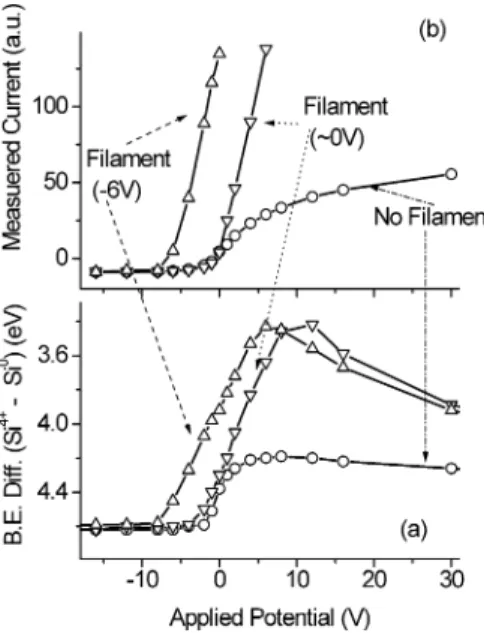
To gain further insight into this process, we had followed the measured binding energy difference between the Si2p peaks of Si4+ and Si0as a function of the applied voltage with the filament off and on as shown in Figure 2 a for a sample containing a thicker (ca. 5 nm) oxide layer. The close resem-blance of the two curves is remarkable. Since we can also apply a bias to the filament, we can affect and shift the energy of the electrons stemming from the filament. As also shown in Figure 2a, we now see that the binding energy difference curve keeps its form but gets shifted by 6 eV, exactly equal to the bias applied to the filament. Since the majority of electrons falling onto the sample stem from the filament, the effect of the stray electrons from the vacuum chamber are overshadowed. In Figure 2b, we plot the measured current falling onto the sample holder as a function of the bias applied to the sample which exhibits a functional dependence similar to the measured binding energy difference. In the same figure the measured current when the filament is turned on is also plotted together with the current
after application of 6 V bias to the filament. Since it is difficult to extract the current falling onto the sample from any other place in the sample rod, the absolute value of it is meaningless. However, their functional dependence on the applied potential is remarkably similar to the binding energy shifts measured (especially the shift with the filament bias). All of these findings strongly support our earlier claim that it is the partial neutraliza-tion by the stray electrons within the vacuum chamber (most probably from the X-ray window), rather than the secondary electrons emitted from the sample, which causes most of the measured bias-induced binding energy differences.20
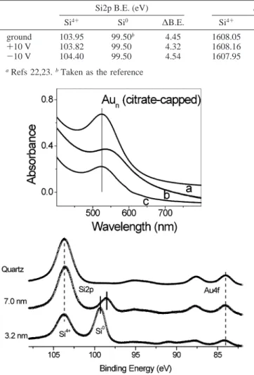
The modified Auger parameter, R, which is defined as the sum of the binding energy of an XPS peak and the kinetic energy of an Auger peak involving the same atomic level, is another instrument for elucidating the physical/chemical nature of the differences measured by XPS. Accordingly, the Auger parameter provides detailed chemical state information, as well as giving a direct measure of the electronic interaction with the surround-ing atoms.24-26Table 1 gives the measured binding and kinetic energies together with the derived Auger parameters of the sample containing 3.5 nm oxide layer without and with external bias. As can be inferred from the table, the measured binding and the kinetic energy differences between the positive and negative 10 V bias are as large as 0.22 eV (definitely larger than our experimental uncertainty which is estimated to be 0.03 eV). However, there is no measurable difference between the derived Auger parameters of the oxide layer and the silicon substrate. This is another proof that the bias-induced differences are related to the differential charging (physical) between the oxide layer and the substrate rather than any chemical differ-ences and biasing is a simple and convenient technique for verification.
Gold Nanoclusters on the SiO2/Si System. As was already demonstrated in our previous report that gold particles deposited by an elecroless process experienced bias-induced shifts similar to that of the oxide layer and not the substrate. Due to the vast amount of recent efforts devoted to the nanocluster-silicon oxide-silicon system, we have extended this investigation to include nanoclusters of gold, prepared by citrate reduction and Figure 1. Si2p region of the XPS spectrum of a silicon sample
containing 3.5 nm oxide layer recorded when the sample was grounded, under +10 V external bias, and when subjected to additional low-energy electrons from a filament nearby (as sketched in the inset).
Figure 2. (a) The Si2p binding energy difference between the Si4+ and Si0of a sample containing ca. 5 nm oxide layer as a function of the applied external potential to the sample rod; (;O;) filament off, (;∇;) filament on but grounded, and (;∆;) when filament is on and biased with -6 V. (b) The current measured falling onto the sample rod in the same format as in (a).
capping.23,27-29In Figure 3, we depict the XPS spectra of the Si2p-Au4f region of citrate-capped gold nanoclusters on silicon containing (i) 3.2 nm and (ii) 7.0 nm oxide layer and on quartz. The same figure also contains the visible spectra of the citrate-capped gold nanoclusters (a) in aqueous solution (as prepared), (b) deposited on quartz, and (c) after transferring the deposited nanoclusters back into the aqueous solution. The strong absorp-tion around 525 nm arising from the plasmon resonance is indicative of nanocluster formation which is red-shifted after deposition on quartz and shifts back to 525 nm after transferring back to the aqueous solution in complete agreement with literature.23, 27-30
Our emphasis is, however, on the XPS spectral shifts, especially to point out that it is the oxide rather than the substrate peak to which Au peaks should be referenced. The measured binding energy differences between the Si2p of the oxide (Si4+) and Au4f7/2of the gold nanoclusters deposited on quartz and silicon substrates containing 7.0 and 3.2 nm oxide are 19.50, 19.38 and 19.47 eV, respectively. Keeping in mind that our precision in measuring difference is better than 0.03 eV, these values are very similar and the small differences arise due to differential charging between the nanoclusters and the oxide layer underneath and/or cluster-size dependent shifts.31-33 However, the measured differential charging between the oxide
layer and the silicon substrate is much larger (in the order of 1 eV). Hence, extreme care has to be exercised for correct choice of binding energy reference. In this particular case of thin (1-10 nm) oxide-substrate system peaks belonging to the oxide layer should be used as the reference and definitely not the substrate.
Figure 4 is a further emphasis of this point depicting that the bias-induced shift in the Si2p and Au4f are shifting together (in sign and magnitude) when an external bias is applied. A positive 10 V bias reduces the binding energy difference between the oxide and the substrate by 0.25 and 0.05 eV when the oxide thickness is 5.2 and 1.5 nm, respectively, parallel to the shifts measured in the Au4f peaks (0.26 ann 0.06 eV, respectively). Similar results are obtained upon application of -10 V.
Acknowledgment. This work is partially supported by TUBA (Turkish Academy of Sciences).
References and Notes
(1) Clarke, R. A.; Tapping, R. L.; Hopper, M. A.; Young. Y. J.
Electrochem. Soc. 1975, 122, 1348.
(2) Hollinger, G.; Jugnet, Y.; Pertosa, P.; Duc, T. M. Chem. Phys. Lett.
1975, 36, 441.
(3) Grunthaner, F. J.; Grunthaner, P. J.; Vasquez, R. P.; Lewis, B. F.; Maserjian, J.; Madhukar, A. Phys. ReV. Lett. 1979, 43, 1683.
(4) Grunthaner, F. J.; Grunthaner, P. J.; Vasquez, R. P.; Lewis, B. F.; Maserjian, J.; Madhukar, A. J. Vac. Sci. Technol. 1979, 16, 1443.
(5) Ishizaka, A.; Iwata, S.; Kamigaki, Y. Surf. Sci. 1979, 84, 355. (6) Hollinger, G. Appl. Surf. Sci. 1981, 8, 318.
(7) Hollinger, G.; Himpsel, F. J. Appl. Phys. Lett. 1983, 44, 93. (8) Wagner, C. D.; Joshi, A.; Gulbrandsen, L.; Deal, B. E. J. Vac. Sci.
Technol. B 1984, 2, 107.
(9) Finster, J.; Schulze, D.; Bechstedt, F.; Meisel, A. Surf. Sci. 1985,
152/153, 1063.
(10) Iqbal, A.; Bates, C. W., Jr.; Allen, J. W. Appl. Phys. Lett. 1985,
47, 93.
(11) Grunthaner, F. J.; Grunthaner, P. J. Mater. Sci. Rep. 1986, 1, 65.
TABLE 1: Measured Si2p Binding and SiKLLKinetic Energies of the Sample Containing a 3.5 nm Oxide Layer, Together with the Modified Auger Parameters (r)a
Si2p B.E. (eV) SiKLLK.E. (eV) R (eV)
Si4+ Si0 ∆B.E. Si4+ Si0 ∆K.E. Si4+ Si0 ∆K.E.
ground 103.95 99.50b 4.45 1608.05 1616.40b -8.35 1712.00 1715.90 -3.90
+10 V 103.82 99.50 4.32 1608.16 1616.40 -8.24 1711.98 1715.90 -3.92
-10 V 104.40 99.50 4.54 1607.95 1616.40 -8.45 1711.99 1715.90 -3.91
aRefs 22,23.bTaken as the reference
Figure 3. XPS spectra recorded after deposition of citrate-capped gold clusters on quartz and silicon samples containing 7.0 and 3.2 nm oxide layers, respectively. The inset shows the visible spectra of the gold nanoclusters (a) in aqueous solution, (b) deposited on quartz, and (c) after transferring the deposited clusters from the quartz back to aqueous solution.
Figure 4. XPS spectra of 2 silicon samples with 1.5 and 5.2 nm oxide layers and gold nanoclusters without and with application of +10 V bias.
(12) Iwata, S.; Ishizaka, A. J. Appl. Phys. 1996, 79, 6653.
(13) Zhang, K. Z.; Greeley, J. N.; Banaszak Holl, M. M.; McFeely, F. R. J. Appl. Phys. 1997, 82, 2298.
(14) Zhang, K. Z.; Banaszak Holl, M. M.; McFeely, F. R. J. Phys. Chem.
B 1998, 102, 3930.
(15) Kobayashi, H.; Kubota, T.; Kawa, H.; Nakato, Y.; Nishiyama, N.
Appl. Phys. Lett. 1998, 73, 933.
(16) Browning, R.; Sobolewski, M. A.; Helms, C. R. Phys. ReV. B 1988,
38, 13407.
(17) Pasquarello, A.; Hybertson, M. S.; Car, R. Phys. ReV. B 1996, 53, 10942.
(18) Dickinson, T.; Povey, A. F.; Sherwood, P. M. A. J. Electron
Spectrosc. Relat. Phenom. 1973, 2, 441.
(19) Howercraft, N. J.; Sherwood, P. M. A. Surf. Interface Anal. 2000,
29, 232.
(20) Ulgut, B.; Suzer, S. J. Phys. Chem. B 2003, 107, 2939. (21) Mitchell, D. F.; Clark, K. B.; Bardwell, J. A.; Lennard, W. N.; Massoumi, G. R.; Mitchell, I. V. Surf. Interface Anal. 1994, 21, 44.
(22) Enustun, B. V.; Turkevich, J. J. Am. Chem. Soc. 1963, 85, 3317. (23) Cumberland, S. L.; Strouse, F. Langmuir 2002, 18, 269.
(24) Wagner, C. D. Anal. Chem. 1972, 44, 972.
(25) Wagner, C. D.; Joshi, A. J. Electron Spectrosc. Relat. Phenom.
1988, 47, 283.
(26) Barranco, A.; Yubera, F.; Espinos, J. P.; Gonzalez-Elippe, A. R.
Surf. Interface Anal. 2001, 31, 761.
(27) Alvarez, M. M.; Khoury, J. K.; Schaaff, T. G.; Shafigulin, M. N.; Vezmar, I.; Whetten, R. L. J. Phys. Chem. B 1997, 101, 3706.
(28) Taleb, A.; Petit, C.; Pileni, M. P. J. Phys. Chem. B 1998, 102, 2214.
(29) Templeton, A. C.; Pietron, J. J.; Murray, R. W.; Mulvaney, P. J.
Phys. Chem. B 2000, 104, 564.
(30) Shipway, A. N.; Lahav, M.; Gabai, R.; Willner, I. Langmuir 2000,
16, 8789.
(31) Wertheim, G. K.; DiCenzo, S. B.; Youngquist, S. E. Phys. ReV.
Lett. 1983, 51, 2310.
(32) Shabtai, K.; Rubinstein, I.; Cohen, S. R.; Cohen, H. J. Am. Chem.
Soc. 2000, 122, 4959.
(33) Ohgi, T.; Sheng, H. Y.; Dong, Z. C.; Nejoh, H.; Fujita, D. Appl.
Phys. Lett. 2001, 79, 2453.